

Page 1
CRT AND LCD SEMI-GRAPHIC DISPLAY PROCESSOR
.
CMOS SINGLE CHIP CRT AND LCD DISPLAYPROCESSOR
.
BUILTIN6 KBYTERAM
.
25 ROWSOR MOREOF40 CHARACTERS
.
CRTMODE :
- ANALOGY LUMINANCE OUTPUT OF 4BIT DAC
- R,G,BDIGITALCOLOROUTPUTS
- FAST BLANKING OUTPUT FOR VIDEO
SWITCHCOMMAND
- SYNCHRONIZATIONINPUTANDOUTPUT
- MASTERAND SLAVE SYNCHRONIZATION
MODES
.
LCDMODE :
- 8 GREYLEVELS
- 4 BITDATAWITH CLOCK OUTPUT
- 3 OUTPUTS FOR LCD DRIVERS SYNCHRONIZATION
- CONTRAST ANALOG COMMAND WITH
DAC OUTPUT
.
128 ALPHANUMERIC CODES AND 128
SEMI-GRAPHICCODES IN INTERNAL ROM
.
PARALLEL ATTRIBUTES THANKS TO 2
BYTE CODES
.
128 ALPHANUMERIC AND 96 SEMIGRAPHIC USER DEFINABLE CODES
DOWN-LOADABLE IN RAM
.
3-WIRE ASYNCHRONOUS SERIAL MCU INTERFACE
.
SQUARE WAVE OR LOGICAL PROGRAMMABLE OUTPUT
.
FULLY PROGRAMMABLE WITH 7 16-BIT
CONTROLREGISTERS
.
24-PINSO OR 20-PINDIP PACKAGES
STV9410
Using its 3-wire serial interface, working in both
read andwritemodeto program7 controlregisters
and to access internal RAM, STV9410 is a highly
flexibleprocessor.
TheSTV9410providesthe useran easytouseand
costeffectivesolutionto display alphanumericand
semigraphicInformationonCRTand LCDscreens.
DIP20
(Plastic Package)
ORDER CODE : STV9410P
DESCRIPTION
STV9410controlleris a VLSICMOS Display Processor. Time base generator, display control & refresh logic, interface fortransparent MCU memory
access,ROM character sets, memoryto store display data & page codes and control registers are
gathered on a single chip component packed in a
short 20 DIPor SO plastic package.
April 1996
SO24
(Plastic Micropackage)
ORDER CODE : STV9410D
1/25
Page 2
STV9410
PIN CONNECTIONS
DIP20
CRT LCD
XTO
XTI
CKO
POR
NCS
SDA
SCK
V
REF
V
SSA
V
SS
1
2
3
4
5
6
7
8
9
10
20
19
18
17
16
15
14
13
12
11
V
DD
V
DD
SYNC IN CKD
V
C
-
I
B
G
R
Y
SYNC
SYNC
FRAME
LOAD
DF
D0
D1
D3
D2
V
EE
RESERVED
XTO
XTI
CKO
POR
NCS
SDA
SCK
V
REF
V
SSA
V
RESERVED
1
2
3
4
5
6
7
8
9
10
11
SS
12
PIN DESCRIPTION
o
Symbol
CRT MODE
- - 1 - Reserved
XTO 1 2 O Crystal oscillator output
XTI 2 3 I Crystal oscillator or clock input
CKO 3 4 O Clock output
POR 4 5 O Programmable output port
NCS 5 6 I Serial interface selection
SDA 6 7 I/O Serial data input/output
SCK 7 8 I Serial interface clock input
V
REF
V
SSA
V
SS
- - 12 - Reserved
- - 13 - Reserved
Y 11 14 O Luminance output
R 12 15 O Red output
G 13 16 O Green output
B 14 17 O Blue output
I 15 18 O Fastblanking output
- 16 19 O Reserved
C
SYNC
V
SYNC
SYNC IN 19 22 I/O Synchro input
V
DD
- - 24 - Reserved
Pin n
DIP20 SO24
I/O Description
8 9 I Resetinput and ref supply of Y DAC
9 10 S Ref ground of Y DAC
10 11 S Ground
17 20 O Composite synchro output
18 21 O Vertical synchro output
20 23 S +5v powersupply
SO24
CRT LCD
24
-
V
23
22
21
20
19
18
17
16
15
14
13
DD
SYNC IN
V
SYNC
SYNC
C
-
I
B
G
R
YV
-
RESERVED
V
DD
CKD
FRAME
LOAD
DF
D0
D1
D3
D2
EE
RESERVED
9410-01.EPS - 9410-02.EPS
9410-01.TBL
2/25
Page 3
PIN DESCRIPTION(continued)
o
Symbol
LCD MODE
- - 1 - Reserved
XTO 1 2 O Crystal oscillator output
XTI 2 3 I Crystal oscillator or clock input
CKO 3 4 O Clock output
POR 4 5 O Programmable output port
NCS 5 6 I Serial interface selection
SDA 6 7 I/O Serial data input/output
SCK 7 8 I Serial interface clock input
V
REF
V
SSA
V
SS
- - 12 - Reserved
- - 13 - Reserved
V
EE
D2 12 15 O D2 Data output
D3 13 16 O D3 Data output
D1 14 17 O D1 Data output
D0 15 18 O D0 Data output
DF 16 19 O LCD polarity output
LOAD 17 20 O Load output (line)
FRAME 18 21 O Frame output
CKD 19 22 I/O Data Clock
V
DD
- - 24 - Reserved
Pin n
DIP20 SO24
I/O Description
8 9 I Resetinput and ref supply of contrast adjustment
9 10 S Ref ground of contrast adjustment
10 11 S Ground
11 14 O Constrast adjustment
20 23 S +5v powersupply
STV9410
9410-02.TBL
BLOCK DIAGRAM
GENERATOR
SYNC
IN
TIME BASE
INTERFACE
NCS SDA SCK
CLOCK
MCU
V
DD
CONTROL
PROCES SING
DISPLAY
LOGIC
6K BYTE
RAM
V
SS
PORCKOXTI XTO
V
REF
DAC
V
STV9410
SSA
CRT
MODE
C
SYNC
V
SYNC
I
Y
LCD
MODE
D2, D3, D1R, G, B
LOAD
FRAME
D0
V
EE
DF
CKD (SYNC IN)
9410-03.EPS
3/25
Page 4

STV9410
ABSOLUTEMAXIMUMRATINGS
Symbol Parameter Value Unit
* Supply Voltage -0.3, +7.0 V
V
DD
* Input Voltage -0.3, +7.0 V
V
IN
T
oper
T
stg
P
tot
* with respect to V
ELECTRICALCHARACTERISTICS
=5V,VSS=0V,Ta= 0 to +70oC, fxtal = 8 to 10MHz, unlessotherwise specified)
(V
DD
Symbol Parameter Min Typ Max Unit
V
DD
I
DD
INPUTS
NCS, SDA, SCK, SYNC IN, XTI
V
IL
V
IH
I
IL
C
IN
V
REF
V
rh
V
rst
R
IN
V
SSA
OUTPUTS
SDA, C
V
OL
V
OH
Y
L
I
L
D
Z
OUT
T
p
* no load on outputs
Operating Temperature 0, +70
Storage Temperature -40, +125
Power Dissipation 300 mW
SS
Supply voltage 4.75 5.0 5.25 V
Supply current * - - 50 mA
Input low voltage 0 - 0.8 V
Input high voltage (except XTI) 2 - V
Input leakage current (except XTI) (0 < VIN<VDD) -10 - +10 µA
Input capacitance (except XTI) - 10 - pF
Voltage reference of DAC 1.5 - V
Reset level on V
V
to V
REF
internal resistance 0.4 - 1.0 kΩ
SSA
REF
0 - 0.4 V
Reference level of DAC 0 - V
SYNC,VSYNC
, R, G, B, I, SYNC IN, DF, XTO, CKO, POR
Output low voltage (IOL= 1.6mA) 0 - 0.4 V
Output high voltage (IOH= - 0.1mA ) 0.8 V
Output voltage (V
REF
=5V, V
SSA
=0, I
OUT
=0)
-VDDV
DD
Integral linearity - - 0.25 V
Differential linearity - - 0.1 V
Output impedance - - 0.5 kΩ
Propagation time at V
OUT
=20pF, I
C
L
90% of V
OUT
FINAL
=0, V
,
REF
=5V, V
SSA
=0V
- - 80 ns
DD
DD
DD
o
C
o
C
9410-03.TBL
V
V
V
9410-04.TBL
4/25
Page 5
STV9410
TIMINGS
=5V±5%, VSS=0V,Ta= 0 to + 70oC, fxtal = 8 to 10MHz,
(V
DD
= 0.8V,VIH=2V,VOL= 0.4V,VOH= 2.4V,CL=50pF,unless otherwisespecified)
V
IL
Symbol Parameter Min Typ Max Unit
SERIAL INTERFACE NCS, SCK, SDA (Figure 1)
T
csl
T
sch
T
scl
f
SCK
T
sds
T
sdh
T
sdv
T
sdx
T
sdz
T
read
OSCILLATOR INPUT (XTI) (Figure 1)
T
wh
T
wl
F
clk
RESET (V
T
res
OUTPUT SIGNALS SDA, C
T
ph,Tpl
T
skew
NCS low to SCK fallingedge 0 ns
SCK pulsewidth high 80 ns
SCK pulsewidth low 80 ns
Serial Clock Frequency 4 MHz
Set up time of SDA on SCK rising edge 20 ns
Hold time of SDA after SCK rising edge 20 ns
Access time in read mode 50 ns
Hold data in read mode 0 ns
Serial interface disable time 50 ns
Delay before Valid Data 2 µs
Clock high level 30 ns
Clock low level 30 ns
Clock frequency 8 10 MHz
)
REF
Reset Low level pulse 2 µs
SYNC,VSYNC
, R, G, B, I, SYNC IN, DF, XTO, CKO, POR (Figure 2)
Propagation time CL=30pF
= 100 pF
C
L
100
Skew between R, G, B,I signals 30 ns
50
ns
ns
(VDD=5V±5%, VSS=0V,Ta= 0 to + 70oC, fxtal = 8 to10MHz,
= 0.2VDD,VOH=0.8VDD,CL=100pF,unless otherwisespecified)
V
OL
LCD INTERFACE D0, D1, D2, D3, CKD, LOAD, DF, FRAME (Figure 3)
t
CYC
t
t
t
WLD
t
t
t
t
SUF
CH
CL
SU
DH
DF
CKD Shift Clock Period 4 x Pxtal ns
CKD Clock High 150 ns
CKD Clock Low 150 ns
Load Pulse Width 150 ns
Data Set-up Time 150 ns
Data HoldTime 150 ns
DF Delay from Load 100 ns
Frame Set-up before Load 150 ns
9410-05.TBL
5/25
Page 6
STV9410
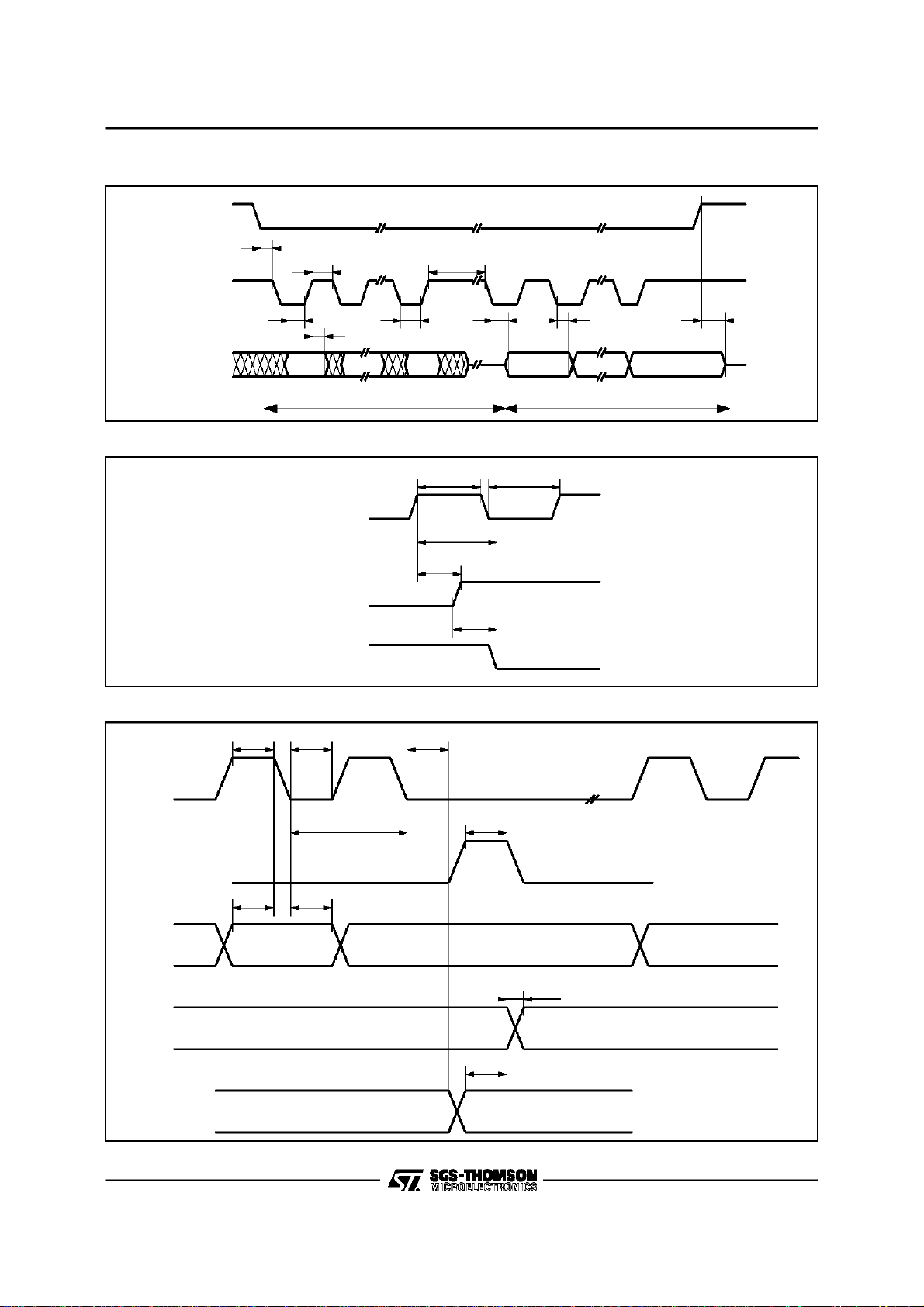
Figure1 : MicrocontrollerInterfaceTimings
NCS
t
csl
t
sch
SCK
t
sds
SDA
A8 A9 A6 A7 D0 D1 D6 D7
Figure2 : Output Signals Delay versus Clock
t
scl
t
sdh
WRITE READ
t
read
t
sdv
t
sdx
t
sdz
9410-04.EPS
Figure3 : LCD Interface Timings
CKD
LOAD
t
CH
t
SU
t
CL
t
DH
XTI
OUTPUT
OUTPUT
t
CYC
t
t
CLD
ph
t
wh
t
pl
t
skew
t
WLD
t
wl
9410-05.EPS
6/25
D0, D1
D2, D3
DF
FRAME
t
SUF
t
DF
9410-06.EPS
Page 7

STV9410
2. FUNCTIONALDESCRIPTION
STV9410displayprocessoroperationis controlled
by a host microcomputervia a 3-wire serial bus. It
is fully programmable through seven internal
read/write registers and performs all the display
functions either for CRT screen or LCD passive
matrix by generatingpixels from data stored in its
internal memory. In addition, the host microcomputer can have straightforward accesses to the
on-chip 6 Kbytes RAM, even during the display
operation.
The following functions are integrated in the
STV9410:
- Crystal oscillator,
- Programmable timing generator,
- Microcomputer3-wire serial interface,
- ROM charactergeneratorincluding128alphanumeric and 128 semigraphic character sets,
- 6 Kbyteson chipRAM to storecharactercodes,
user definable character sets, and any host microcomputerdata,
and in CRT mode :
- Y outputdriven by a 4-bitDAC,
- Programmablemaster or slave synchromodes,
- R, G, B,I outputs,
in LCD mode:
- LCD interface for passive multiplexedmatrix,
- 7 grey levels plus black.
2.1 SERIALINTERFACE
This 3-wire serial interface can be used with any
microcomputer.Datatransferissupportedbyhardware peripherals like SPI or UART and can be
emulated with standard I/O port using software
routine ( seeapplicationnote ).
NCSinputenablestransferonhighto lowtransition
and transfer stays enabled as long as NCS input
remains at logical low level. NCS input disables
transfer as soon as low to high transition occurs,
whatever transfer state is, and transfer remains
disabled as long as NCS input remains at logical
high level.
SCKinput receives serial clock; it must be high at
the beginning of the transfer; data is sampled on
rising edge of SCK.
SDAinput(in writemode)receivesdatawhichmust
be stable at least t
before and at least t
sds
sdh
after
SCK rising edge. In read mode, SDA receives
address and read command (R/W bit) and then it
switches from input state to output state to send
data (seeData transferand ApplicationNote).
Data Transfer in Write Mode
The host MCU writesdata into STV9410registers
or memory.TheMCU sendsfirstMSBaddresswith
R/W bit clear, it sends secondly LSB address followed by data byte(s). STV9410, then, internally
incrementsreceived address,readyto storeasecond databyteif needed,and soon, aslongasNCS
remainslow (see Figure 4). LSBare sent first.
Data Transfer in Read Mode
The host MCUreads data from STV9410 registers
or memory.TheMCU sendsfirstMSBaddresswith
R/W bit set, it sends secondly LSB address, then
SDA pin switches from input state to output state
and providesdatabyte(s) at SCK MCU clock rate.
Notice that a minimum delay is needed before
sendingthefirst SCKrisingedgeto sample the first
data bit (at least 2µs). After each data byte
STV9410 internally increments address and it
sendsnextdataatSCKfrequency.SDAremainsin
output state as long as NCS remains low (see
Figure5).
Address auto-incrementation allows host MCU to
use 8, 16, 32-bit data words to optimize transfer
rate. LSBare sent first. SCK max speed is 4MHz.
7/25
Page 8
STV9410
Figure4 : Serial InterfaceWrite Mode
NCS
SCK
SDA
A8 A9 A10 A11 A12 A13 W A0 A1 A2 A3 A4 A5 A6 A7 D0 D1 D2 D3 D4 D5
@ MSB @ LSB Data byte 1
NCS
SCK
D5 D6 D7 D0 D1 D2 D3 D4 D5 D6 D7
SDA
Figure5 : SerialInterface Read Mode
NCS
SCK
SDA
A8 A9 A10 A11 A12 A13 R A0 A1 A2 A3 A4 A5 A6 A7 D0 D1 D2 D3 D4 D5
data byte ndata byte n - 1
9410-07.EPS
2µs min.
SDA Pin
8/25
@ MSB @ LSB Data byte 1
INPUT OUTPUT
NCS
SCK
D5 D6 D7 D0 D1 D2 D3 D4 D5 D6 D7
SDA
data byte ndata byte n - 1
SDA Pin
OUTPUT
INPUT
9410-08.EPS
Page 9

STV9410
2.2. ADDRESSING SPACE
STV9410registers,RAMandROM are mapped in
a 12 kbytesaddressing space.Themapping is the
following:
0000h
Display memory
DRCS
Descriptor tables
User memory
17FF h
1800h
1FFF h
2000h
24FF h
2500h
27FF h
2800h
2CFF h
2D00h
2FEF h
2FF0 h
2FFF h
6144 RAM
bytes
Empty
Area
1280 slices
ROM G0
Empty
Area
1280 slices
ROM G1
Empty
Area
Internal
Registers
2.2.1 Register Set
VERT
2FF1 LCD ILC C/H V/P VSE HSE - F8
2FF0 F7 F6 F5 F4 F3 F2 F1 F0
LCD : LCD/CRT mode
ILC : Interlaced/non-interlaced
C/H : Composite/horizontalsynchro
V/P : Verticalsynchro/real time port
VSE : Vertical synchro enable
HSE : Horizontal synchro enable
F (8:0) : Number of scan line per frame
HORI
2FF3 -----MG2MG1MG0
2FF2 - - L5 L4 L3 L2 L1 L0
MG (2:0): Margin duration
L (5:0) : Line duration
HSYN
2FF5 SU7 SU6 SU5 SU4 SU3 SU2 SU1 SU0
2FF4 SD7 SD6 SD5 SD4 SD3 SD2 SD1 SD0
SU (7:0) : Synchro rising edge position
SD (7:0) : Synchro falling edge position
POR
2FF7 VOE - - - - - TE PV
2FF6 N7 N6 N5 N4 N3 N2 N1 N0
VOE : Video output enable
TE : Timer enable
PV : Port value
N (7:0) : Square wave period
ADDR
2FF9 - P12 P11 P10 P9 P8 P7 P6
2FF8 - G12 G11 G10 - A12 A11 A10
P (12:6) : Address of first descriptor of page to display
G (12:10) : User definable graphiccharacter set address
A (12:10) : User definable alphanumeric character set
address
DISP
2FFB IMG GMG RMG BMG - - - HIC
2FFA FLE CCE IN1 IN2 BR3 BR2 BR1 BR0
IMG, GMG,
RMG, BMG
HIC : High contrast, forces black and white on
FLE : flashing enable
CCE : Conceal enable
IN1, IN0 : Fast blanking mode
BR (3:0) : Luminosity adjustment on Youtput
: Margin value of I, G, R, B outputs
outputs
CURS
2FFD CEN CBL CUL - C12 C11 C10 C9
2FFC C8 C7 C6 C5 C4 C3 C2 C1
CEN : Cursor enable
CBL : Cursor blinking
CUL : Cursor underlining
C (12:1) : Cursor address
9/25
Page 10

STV9410
2.2.2 Descriptor
UNIFORM
MSB 0 RTP FFB - I C2 C1 C0
LSB SL7 SL6 SL5 SL4 SL3 SL2 SL1 SL0
RTP : Real time port
FFB : Field flyback
I : Fast blanking
C (2:0) : Strip color (G, R, B)
SL (7:0) : Number of scan line of the strip
CHARACTER
MSB 1 RTP DE ZY C12 C11 C10 C9
LSB C8 C7 C6 C5 C4 C3 C2 C1
RTP : Real time port
DE : Display enable
ZY : Vertical zoom
C (12:1) : Address of first character to display
2.2.3 Code Format
ALPHANUM
MSB
(ODD)
LSB
(EVEN)
CHARACTER NUMBER : lower than 80h in ROM
IV : Inverted video
DW : Double width
DH : Double height
FL : Flashing
FC (2:0) : Foreground color (G, R, B)
0 IV DW DH FL FC2 FC1 FC0
CHARACTER NUMBER
from 80hto FFh in RAM
GRAPHIC
MSB
(ODD)
LSB
(EVEN)
CHARACTER NUMBER : lower than 80h in ROM
BC (2:0) : Background color (G, R, B)
FL : Flashing
FC (2:0) : Foreground color (G, R, B)
1 BC2 BC1 BC0 FL FC2 FC1 FC0
CHARACTER NUMBER
from 80hto DFh in RAM
CONTROL
MSB
(ODD)
LSB
(EVEN)
EOL : End of line
IF, IB : Fast blanking foreground/background
UL : Underline
CC : Conceal
BC (2:0) : Background color (G, R, B)
HG : Hold graphic
FC (2:0) : Foreground color (G, R, B)
1 1 1 EOL IF IB UL CC
1 BC2 BC1 BC0 HG FC2 FC1 FC0
2.2.4 Example of RAM Maping
0000h
0040h
0080h
00A8h
07D8h
0800h
1000h
1400h
17FFh
Descriptor (Table 1)
(for page 0)
Descriptor (Table 2)
(for page 0)
Page 0 Row 1
Code 0 to 39
Page 0 Row 2
Code 0 to 39
~
~
Page 0 Row 24
Code 0 to 39
Descriptor (Table 1)
(for page 1)
Descriptor (Table 2)
(for page 1)
Page 1 Row 1
Code 0 to 39
Page 1 Row 2
Code 0 to 39
~
~
Page 1 Row 24
Code 0 to 39
Alphanum Character 0
Alphanum Character 1
~
~
Alphanum Character 93
Page 0 Row 0
Code 0 to 39
Free
Graphic Character 0
Graphic Character 1
~
~
Graphic Character 93
Page 1 Row 0
Code 0 to 39
Free
64b
64b
80b
80b
~
~
80b
64b
64b
80b
80b
~
~
80b
10b
10b
~
~
10b
80b
10b
10b
~
~
10b
80b
4b
4b
2 Kbyte
~
~
2 Kbyte
~
~
~
~
1 Kbyte
~
~
1 Kbyte
9410-09.EPS
10/25
Page 11

STV9410
2.3 CLOCKAND TIMING GENERATOR
The whole timing is derived from XTI input frequency which can be an external generator or a
crystal signal thanks to XTO/XTI oscillator.This
clock is also pixel frequencywhich can be chosen
between 8MHz to 10MHz (pxlck). This clock is
availableon CKOpin.It shouldbeusefor theMCU,
savinga crystalin the application.
The activeareaof a video lineis 320 pixelsperiods
long (40 characters of 8 pixels wide). Number of
linesperframe,marginwidth,line duration,leading
and trailingedgesofhorizontalsynchronizationare
fully programmable in CRT mode using VERT,
HORI, HSYN registers.
A RESET, can be applied to STV9410 by pulling
low V
pin ( ≤ 0.4V).
REF
On RESET, default values are forced into configuration registersand video outputsare at low level.
All unusedbit of registers arealways readas ”0”.
Figure 6 : VertRegister Scan Lines Programmation
LCD ILC C/H V/P VSE HSE - F8 F6 F5F7 F4 F3 F2 F1 F0
XXXXXX-0 00000000
000000001
0
0000 0111
000 011111
0 011 000 01
001101101
000000000
1
F[8:0] = Scan Line Number- 2
2.3.1 Time Base Registers
VerticalTime Base and Configuration
Register (VERT)
Internaladdress : 2FF1-2FF0h
RESETvalue :01-36h
(@ = RESET default configuration)
2FF1 h LCD ILC C/H V/P VSE HSE - F8
@ 00000001
2FF0 h F7 F6 F5 F4 F3 F2 F1 F0
@ 00110110
LCD : 1 LCD mode
ILC : 1 Interlacedscanning
C/H : 1 C
V/P : 1 V
VSE : 1 enable vertical synchro with SYNC IN
HSE : 1 enable horizontal synchro with SYNC IN
F (8:0) : scan line number per frame (@ 312)
111
1111
0 CRTmode @
0 non-interlaced scanning @
is composite synchro
SYNC
0C
0V
is horizontal synchro @
SYNC
is vertical synchro
SYNC
is RTP bit of current descriptor @
SYNC
0 disable @
0 disable @
2FF02FF1
0
11011110
0
00111110
011
0
01
01
1
0100 110
01
0
11011100
11011100 1
0
11111100
0
11111110
0
1111
11111
Nb ofS can
Lines
F(0:8) + 2
Not allowed
3
16
64
100
120
240
250
262
263
310
312
313
320
480
512
513
LSB
HEXA
-
01
0E
3E
62
76
EE
F8
04
05
34
36
37
3E
DE
FE
FF
9410-10.EPS
11/25
Page 12

STV9410
Margin and HorizontalTimeBase
HorizontalSynchronizationRegister (HSYN)
Register (HORI)
Internal address : 2FF3-2FF2h
RESETvalue :03-3Fh
(@ = RESET defaultconfiguration)
2FF3 -----MG2MG1MG0
@ 00000011
2FF2 - - L5 L4 L3 L2 L1 L0
@ 00111111
MG(2:0) : Left and right marginduration (@ = 4µs)
L(5:0) : Line duration (@= 64µs)
MG =
LineDuration
L=
MarginDuration
8 pxlck
− 1
8 pxlck
− 1
Internaladdress : 2FF5-2FF4h
RESETvalue :E6-DCh
(@ = RESET default configuration)
SU(7:0) : SYNC rising edge position (@= 57.75µs)
SD(7:0) : SYNC falling edge position (@= 53.25µs)
Figure 7 : HSYNRegister SynchroPulse Programmation
Qz = 8MHz
REG
HORI
Active area
2FF5 SU7 SU6 SU5 SU4 SU3 SU2 SU1 SU0
@ 11100110
2FF4 SD7 SD6 SD5 SD4 SD3 SD2 SD1 SD0
@ 11010100
RiseEdge Position
SU =
FallingEdge Position
SD =
2 pxlck
2 pxlck
Register
Value
(L = 3F)
− 1
− 1
Duration
(µs)
64µs
Duration
(nber of char.)
64
FIXED
HORI
FIXED
RESULT
HSYN
HSYN
HSYN PULSE
HSYN
HSYN
HSYN PULSE
(MG = 0)
(SU = B7)
(SD = BF)
Positive Pulse
(SU = BF)
(SD = B7)
Negative Pulse
1µs
1µs
40µs
21µs
46µs
48µs
48µs
46µs
1
1
40
21
46
48
48
46
9410-11.EPS
12/25
Page 13

Figure 8 : Horizontal SynchronizationTiming
STV9410
TIMING DIAGRAMDESIGNATION COMMENTS
PIXEL CLOCK
START
Y OUTPUT
START
”HORT” MSB REG
”HORT” LSB REG
”HSYN” LSB REG
”HSYN” MSB REG
HSYN PULSE
0 Start Margin Active Area (320 pixels)
VideoValidationand Port Register(PORT)
Internaladdress :2FF7-2FF6h
RESETvalue:00-00 h
(@ = RESETdefault configuration)
2FF7 VOE -----TEPV
@ 00000000
2FF6 N7 N6 N5 N4 N3 N2 N1 N0
@ 00000000
VOE : Video Output Enable
TE : Timer Enable
PV : Port Value
N(7:0) : Square wave period on POR if TE=1 (@=0)
1 enable synchro & video outputs
0 disable synchro & video outputs @
(@ Output Y,C
and DF are grounded, Input SYNC IN is high
impedance)
1 POR provides a square wave signal with a
period of 16 x N(7:0) x pxlck
0 POR output is PV bit @
POR output value if TE=0 (@=0)
SYNC,VSYNC
, R, G, B, I, POR,
BEWARE
The programmationof VERT, HORI, HSYN regis-
tersmust beconsistent.Togetaproperworkof the
controller, the following conditions must, in any
Crystal = 8MHz
pxlck = 125ns
Margin End of line 0
0 = origin
DAC output
8pxlck Fixed
= (MG +1) x 8 x pxlck
= (L +1) x 8 x pxlck
= (SD + 1) x 2 x pxlck
= (SU + 1) x 2 x pxlck
mode (CRT or LCD), be fulfiled:
-SU≠SD
SU+ 1
-
4
<L and
SD+ 1
4
<L
- 2(MG + 1) +40 ≤ L
Line periodis :
=[L(5:0) + 1] x 8 pxlck
-P
L
- In LCD, MG(2:0) can be 0, then minimum Line
Periodis P
L (min.)
=43 x 8 pxlck
Frame period is :
-P
= [F(8:0) + 2] xP
F
L
- In LCD, using a 240 lines matrix, F(8:0) = 238,
then minimum frameis :
P
= 240 x 43 x8 pxclk
F (min.)
Pixelperiod is :
P
- Pxclk =
[F(8:0)+2][L(5:0)+1] x8
Frame
- I n LCD, u sing a 240 lines m atrix, and
P
MG(2:0)= 0, Pxclk=
Frame
240 x 43 x 8
Interlacedmode conditions:
SU+ 1
-
SU+ 1
-
4
4
and
and
SD+ 1
4
SD+ 1
4
<L
>(MG + 1) +42
9410-12.EPS
13/25
Page 14

STV9410
2.3.2. CRTMode
In CRTmode, the Vsyncsignal appearsat the first
two lines of the first strip of the descriptor list. It is
recommendedto provide an uniformblanked(with
FFB bit) strip as first descriptor. The scan line
numberof thisstrip have to be equal or higher than
scan line number of the verticalblanking Interval.
Master Mode
This mode is selectedby writing VSE and HSE bit
of VERTregisterwith logicalvalue ”0”.
Non-interlacedmode is selectedbywritingILCbit
vertical time base counterF(8:0) of VERTregister
is reset withoutany modificationof othertime base
registers.
HorizontalSynchronization
SYNC IN is sampled one pxlck before and one
pxlck after internal horizontal pulse transition. If
fallingedge is not found,one pixel period isadded
to internal line duration. Using a line frequency
locked clock applied on XTI, internal scan line
becomes phase locked after few scan line periods
at programmedvalue (see Figure11).
of VERTregisterwith logicalvalue ”0”.
Horizontal or composite synchronization signal is
output on C
nal is output on V
pin, Vertical synchronizationsig-
SYNC
pin.
SYNC
Signal waveforms are described in Figure9.
Interlaced mode is selected by writing ILC bit of
VERTregister with logical value ”1”.
Even frame is identical to non-interlaced frame.
V
PULSEis low during secondhalf of last line
SYNC
of previousOddframeandduringthe two firstlines
of current Even frame.
Odd frame is one scan line morethan Evenframe.
V
PULSEis low during the two first lines and
SYNC
up tofirst halfofthe third line of current Odd frame.
Half line corresponds to 17th character position.
Signalswaveforms are describedin Figure10.
2.3.3 LCD Mode
LCD mode only works as a master mode with 320
pixels per line. Internal algorithm allows 8 grey
levels on passive LCD matrix. Numberofscan line
is programmable.In orderto get maximumrefresh
frequencyofdisplay,marginandlinedurationmust
be reduced to miminum. Interlaced mode and externalsynchronizationare not allowed.The1
of the first descriptor in the description list correspond to the firstline of the LCD display. Y output
providesa programmablevoltage usableto adjust
contrast of LCD display. To reduce supply current
consumption,when Y outputisunused,V
not be connectedto ground,andV
a reset pin. Notice that SYNC IN Pin provides
(CKD) data clocksignal.
Slave Mode
This mode is activatedby writing VSE and/or HSE
bit of VERT register with logical value ”1”. Then
SYNC IN input signal is sampled according to
proceduredescribedbelow.
VerticalSynchronization
SYNC IN signal may beeither a verticalsynchronization or a composite synchronization. It is sampled on first pixel of eachscan lineactive area. As
soon as SYNC IN signal low level is detected,
2.4 POROUTPUT
POR is a standardI/O pin programmableat logical
level”1” or”0”. Itcan alsoprovidea programmable
square wave signal of period
P = 16 x N(7:0)x pxlck (0 ≤ N ≤ 255).
It can drive a capacitive buzzer (see application
diagramat page 22).
RESETvalue of PORTis ”0”.
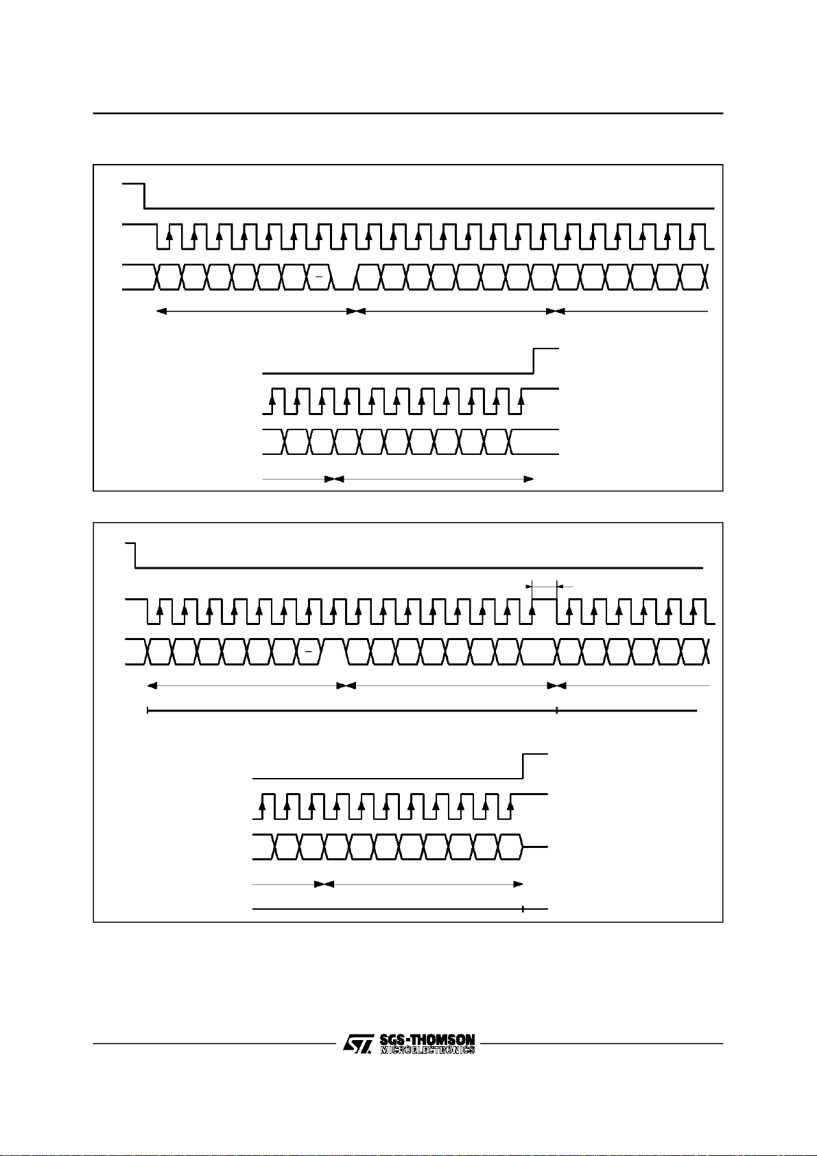
Figure 9 : ODDand EVENSynchronization Pulses in Non-interlacedMode
pinworksas
REF
SSA
st
line
must
DESIGNATION TIMING DIAGRAM COMMENTS
H SYNCPULSE
PULSE
C
SYNC
V
PULSE
SYNC
”VERT” LSB REG
LINENUMBER N N + 1 N + 2
* Internal logic adds one more line
14/25
F
N-1
F
N
F
N+1
F0 F1
*
12F23
F3
4
HorizontalSynchro
CompositeSynchro
Vertical Synchro
Programmedvalue
of F (8 : 0) is N
Framenumber
of lines is N + 2
9410-13.EPS
Page 15

Figure 10 : InterlacedMode SynchronizationPulses
STV9410
DESIGNATION TIMING DIAGRAM COMMENTS
H SYNC PULSE
C
PULSE
SYNC
”VERT” LSB REG
LINENUMBER
F
N- 1
N N+1 N+2
F
F
N
N+1
F0 F1
12
F2
F3
3
4
Horizontal
Synchro
Composite
Synchro
Programmed value
of F (8 : 0)is N
EVEN framenumber
of lines is N + 2
PreviousPicture CurrentPicture
SYN C
EVENFrame ODD Frame
PULSEV
Vertical Synchro
ODD Frame
Horizontal
H SYNCPULSE
C
PULSE
SYN C
”VERT” LSB REG
LINE NUMBER
PULSEV
SYN C
F
N
N+1
ODD Frame
F
N+1
N+2 N+3
F
N+2
F0 F1
12
Current Picture
F2
3
EVEN Frame
F3
4
Synchro
Programmed value
of F (8 : 0)is N
ODD frame number
of lines is N+ 3
Picture number
of lines is 2N + 5
Vertical Synchro
EVEN Frame
ZONE
CHAR NUMBER
H SYNCPULSE
LINE 3
ODD FRAME
LINE N + 3
ODD FRAME
Start Margin Active Area Margin End of line
1 2 15 16 17 39403 4 18 38
Characters
Position
Horizontal
Synchro
Composite
Synchro
Composite
Synchro
9410-14.EPS
15/25
Page 16

STV9410
Figure11 : Synchronizationon SYNC IN ExternalSignal
VERTICALSYNCHRONIZATION
DESIGNATION
TIMINGDIAGRAM
COMMENTS
PIXELCLOCK
Y OUTPUT
SYNCIN
VERTICAL
PULSE
F(8:0)
DESIGNATION
PIXELCLOCK
INTERNALH SYNC
DURATION= L (5 : 0)
EXTERNALH SYNC
UNLOCKED
EXTERNALH SYNC
LOCKED
H Pulse
Sampling
Clock
Margin
x
SF
Active Area
HORIZONTALSYNCHRONIZATION
TIMINGDIAGRAM
Margin
H Pulse
Samplingon
first pixel of
F
0
L= L+ 1
L=L
active area
S = 0 clear
F (8 : 0) only
COMMENTS
Sampling
Clock
Samplingwindow
for H Synchro
Line Duration
Increase+ 1
Good
Line Duration
9410-15.EPS
3. INTERNALREGISTER DESCRIPTION
STV9410 is programmable with 7 registers of 16
bit each.Theseregisters canalso be programmed
in byte mode.Not significantbit must be clearedin
order to be compatiblewith next generationproducts.
3.1 TIME BASE REGISTERS
RegistersVERT, HORI,HSYN and PORTare describedin chapter2.3
3.2 ADDRESS REGISTER(ADDR)
Internal address : 2FF9-2FF8h
16/25
RESETvalue :00-00h
(@ = RESET default configuration)
2FF9 h - P12 P11 P10 P9 P8 P7 P6
@ 00000000
2FF8 h - G12 G11 G10 - A12 A11 A10
@ 00000000
P(12:6) : Page first descriptor address, P(5:0)=0 @
G(12:10): Graphic characterset MSB address,
G(9:0)=0 @
A(12:10) : Alphanumeric character set MSB address,
A(9:0)=0 @
NB : asaddressesare in RAMarea,addressbit13
is resetto ”0”
Page 17

Figure 12 : ADDRRegisterand Descriptor List Address
2FF9 2FF8
STV9410
ADDR REGISTER
REALADDRESS
PROGVALUE
REALADDRESS
PROGVALUE
REALADDRESS
PROGVALUE
- P12 P11 P10 P9 P8 P7 P6 - G12 G11 G10 - A12 A11 A10
010000000000000 (0800h)
20
01 0 00000000 (15C0h)
1111
57
010 00 00000000 (0A40h)
29
11
3.3 DISPLAYREGISTER (DISP)
Internal address : 2FFB-2FFAh
RESETvalue :00-00h
(@ = RESET defaultconfiguration)
2FFB IMG GMG RMG BMG - - - HIC
@00 0 00000
2FFA FLE CCE IN1 IN0 BR3 BR2 BR1 BR0
@00 0 00000
Used for RAM character sets
--
--
--
64 bytes blocks
9410-16.EPS
BR(3:0) : This value iscombined with pixelvalue todrive
Y DAC in CRT mode :
Y= 4xG + 2xR + B + BR(2:0)+ 3x(R orG or B)
(logical or)
R, G, B,I, Y,= 0during line flyback.
Black level is output with R, G, B = ”0”.
White level is output with R, G, B = ”1”.
During frameflyback, R, G, B, I, Y provides signal
accordingto uniform strip descriptor FFB bit state
(see chapter 4.2.1)
During LCD mode BR(3:0) drives continuously Y
DAC. Notice that only bit 0 to 2 of BR are used in
CRT mode.
IMG,
GMG,
RMG,
BMG
HIC : Forces alphanumeric characters background
FLE : Flashing enable, 0 = disable @
CCE : Conceal enable, 0 = disable @
IN1,IN0 : Insertion attribute mode selection. Mode
: Margin value of I, G,R,B outputs and
background color and insertion default attribute
of next alphanumeric character. In case of
graphic characters only I is default attribute.
black (R, G, B = 0), and foregroundwhite (R, G,
B = 1) for maximum contrast, 0 = disable @
selects value of I output during active area of
scan line in CRT mode; I output value (during
margin) is programmed with DISP register;
during uniform strip I output value is set
according to strip descriptor.
During active time slot :
0 0 : I output gets value of current code I
attribute (margin attribute or control
character attribute ) @
0 1 : I is set (”1”)
1 0 : I output gets value of current code I
attribute if I=0 R,G,B are reset to ”0”
0 1 : Reserved mode
3.4. CURSOR REGISTER (CURS)
Internaladdress : 2FFD-2FFCh
RESETvalue :00-00 h
(@=RESET default configuration)
2FFD CEN CBL CUL - C12 C11 C10 C9
@ 00000000
2FFC C8 C7 C6 C5 C4 C3 C2 C1
@ 00000000
CEN : Cursor enable, 0 = disable @
CBL : 0 c ursor blinking off, ch aracter blinking
attribute unchanged @
1 cursor blinking on, blinking is mixed with
character blinkingattribute. Blinking frequency
is around 1Hz and duty cycle 50%
CUL : 0 characterunderlineattributiscomplemented
on cursor position @
1 character color is complemented on cursor
position
C(12:1) : Cursor address (not a screen position)
17/25
Page 18

STV9410
4. DISPLAY CONTROL
4.1 SCREENDESCRIPTION
A screen is composed of successive scan lines
gathered in one or several strips. Each strip is
defined by a descriptor stored in memory.A list of
descriptors allows screen composition, different
screenscanbe defined in memory(seeapplication
note and Figures13, 14.).
Two kinds of strip are available:
- Uniform color strip
Applications:
- vertical front and back porch
- vertical synchro
- borderlines
Parameters:
- number of scan lines
- color
- Character strip
Charactersand attributes are definedby a suc-
cessionof codes storedinmemory;thankstothe
charactercode,a memoryaddress iscalculated
and used to get the characterpattern.
Parameters:
- address of the first code
- size, display enable
Figure13 : Programmationof Number of Scan Lines- VerticalRegister VERT(2FF0/2FF1)
and Descriptor List
DESCRIPTORLIST
CONTENTS
SCAN LINES
SUM
1460 A8AA0A02 F8AA 20AB 48AB D0BA 1402 1906 1903 1907
U0* U1 R0* R1 R2 R18 R19 U2 U3 U4 U5
20 10 10 10 10
20 30 40 50 60
10 10 20 25 25 25
220 230 250 275 300 325
VERT REGISTER
COMMENTS
VERT REGISTER
COMMENTS
* U0 is uniformstrip number 0, R0 ischaracter strip number 0
242 Scan Lines(00F0h)
U2 Strip is cut (red uniform strip)
312 Scan Lines (0136h)
U2 (red), U3 (yellow), U4 (cyan) and part of U5 (white) uniform strip are displayed
Figure14 : Relation betweenScreen Location/DescriptorPointer/RAMPage Codes
OTHER
25th ROW CODES
OTHER
1st ROW CODES
3rd ROW CODES
2nd ROW CODES
OTHER
23th ROW CODES
OTHER
Address
of the list
UNIF 0
ROW 0
ROW 1
ROW 2
ROW 22
ROW 2
ROW 24
UNIF1
ADDR
REGISTER
TOP UNIFORM STRIP
1st CHARACTER ROW
2ndCHARACTER ROW
3rd CHARACTERROW
23th CHARACTERROW
24th CHARACTER ROW *
25th CHARACTERROW
BOTTOMUNIFORM STRIP
* Identical to row 2
9410-17.EPS
18/25
PAGE CODES LOCATION
RAM
RAM
DESCRIPTOR LIST
SCREEN
9410-18.EPS
Page 19

STV9410
4.2. STRIP DESCRIPTOR
Each strip is definedby 2 bytes.
During the vertical retrace, an internal descriptor
addresscounterisinitialisedwith the valueP(12:0)
of ADDR register; on the trailing edge of vertical
synchro, the firststrip descriptoris loaded into the
display controller;if it is an uniform strip, selected
colorisdisplayedduringthecorrespondingnumber
of scan lines; if it is a character strip, left margin
followed by text, followed by right margin are displayed during 10 scan lines; the next descriptoris
then read, and the same process is repeated until
the last scan line. This informationbeing given by
the verticaltiming generator.
4.2.1 UniformStrip
0 RTP FFB - I C2 C1 C0
SL7 SL6 SL5 SL4 SL3 SL2 SL1 SL0
RTP : Real Time Port
RTP bit value is outputon V
of VERT register is ”0”, along the complete
duration of the strip scan line.Notusedin LCD
mode.
SYNC
when V/P bit
FFB : Field Flyback
I : 0 Fast Blanking Disable
C(2:0) : G, R, B,value during theactive areaofthe strip
SL(7:0) : Number of scan lines of the strip, minimal
0 R, G, B, I and Y outputs are defined by
corresponding bit of DISP for margin and
C(2:0) and I for active area
1 R, G, B, I and Y outputs are cleared during
Field Flyback,whatever other parameters are.
1 Fast Blanking Enable
(320 pixels)
value is 1.
4.2.2. CharacterStrip
1 RTP DE ZY C12 C11 C10 C9
C8 C7 C6 C5 C4 C3 C2 C1
RTP : Real Time Port
DE : Display Enable
ZY : Vertical Zoom
C(12:1) : Address of the first code to display
RTP bit valueis output on V
of VERT register ”0”, along the complete
duration of the stripline, during the wholestrip.
0 display off,thestripis displayedwithmargin
attributes IMG, GMG, RMG, BMG bit of DISP
register,
1 display on, the strip works as selected.
0 normal display mode
1 allscan line are doubled, providing avertical
zoom effect
when V/P bit
SYNC
Figure15 : Character StripDescriptor- First Character AddressSelection
LSBMSB
DESCRIPTOR 1 RTP DE ZY C12 C11 C10 C9 C8 C7 C6 C5 C4 C3 C2 C1
EFFECTIVEADDRESS
BINARYADDRESS - - - - 1010111110000
1010101011111000BINARYDESCRIP.
PROGVALUE
EFFECTIVEADDRESS
BINARYADDRESS
BINARYDESCRIP.
PROGVALUE
- -- -0100101110010
1110010010111001
AFA8
EB
5
9270
4
F1
0
9
C0
9410-19.EPS
19/25
Page 20

STV9410
5. CHARACTERCODE FORMAT
Each character is defined with a two bytes code;
the first is at an even address,the secondis at the
followingodd address. Some attributes are parallel, other keep the last explicit value.
STV9410 uses 3 differenttypesof codes.
5.1 ALPHANUMERIC CHARACTERS
(256 patterns)
The backgroundcolor is not definedbythe code;it
takes the samevalue as the previouscharacter or
it has the value of the margincoloratthe beginning
of each row.
The characterpattern lies in ROM if CHARACTER
NUMBER is lower than 80h, (ALPHANUMERIC
CHARACTER SETis shown inTABLE3),else it is
User Defined Character in RAM (DRCS).
ODD CHARACTER NUMBER
EVEN 0 IV DW DH FL FC2 FC1 FC0
CHARACTER
NUMBER
IV : Inverted video if set.
DW : Double character width ifset, code must
DH : Double character height if set, code
FL : Flashing, inverted phase if IV is set.
FC(2:0) : Foreground color (Green, Red,Blue).
5.2. GRAPHIC CHARACTERS (224patterns)
IV,DW, DH,UL take the value ”0”
CHARACTER NUMBER must be lower than E0h.
The characterpattern lies in ROM if CHARACTER
NUMBERislowerthan80h,(STANDARDMOSAIC
charactersetisshowninTable4),elseitisanUser
Defined Character in RAM (DRCS).
ODD CHARACTER NUMBER
EVEN 1 BC2 BC1 BC0 FL FC2 FC1 FC0
CHARACTER
NUMBER
BC(2:0) : Background color (Green, Red, Blue).
FL : Flashing.
FC(2:0) : Foreground color (Green, Red,Blue).
5.3. CONTROL CHARACTERS (32 codes)
These characters are displayed as foreground
color spaces if HG bit is clear. They can change
some attributesapplying to themselvesand to the
followingstring.
: ROM orRAM character set code
be repeated for the right part of the
character.
must be repeated for the bottom part of
the character. The first DH attribute
encountered in a vertical column is
always interpreted as a top part.
: ROM orRAM character set code
ODD 1 1 1 EOL IF IB UL CC
EVEN 1 BC2 BC1 BC0 HG FC2 FC1 FC0
EOL : End Of Line
0 normal control code
1 space are displayed untiltheend of the row,
allowing memory space saving
IF,IB : Insert foreground, Insertbackground attribute.
0 fast blanking disable
1 fast blanking enable
UL : Underlined
0 disable
1 enable
CC : Conceal Character
0 disable
1 enable, character is diplayed as a space.
BC(2:0) : Default background color of next character(s)
HG : Hold Graphics
0 disable, the control character is displayed as
a uniform space character with foreground
color fixed by FC(2:0)
1 enable, the control character pattern takes
the last mosaic value encountered in the row,
if any, or is a space.
FC(2:0) : G, R, B foreground value of the control
character
At thebeginningof eachrow,those attributestake
default values :
- EOL, UL, CC, HG = 0
-IF=1
- IB = IMG (Margin insertattribute)
- BC(2:0) = GMG, RMG,BMG (Margincolor).
Notice that following characters code is reserved
for futur use.
ODD1111XXX1
EVEN 1 X XXXXXX
6. CHARACTERGENERATORS
Each pixel is defined with one bit, 1 refers to
foregroundcolor, and 0 to backgroundcolor.
PX7 PX6 PX5 PX4 PX3 PX2 PX1 PX0
PX7 is the leftmost pixel.
Characterslice address :
Eachcharactergeneratorcontainsa successionof
patternsarrangedasa numberofhorizontalslices:
- Slice addr = (Set addr) + Char Number x 10 +
(slicenumber)
- Char Number is the number of the character in
the set; usingDRCS in RAM, the callingcode of
the character is the number of the character in
the set plus 80h.
- Set addr is defined in ADDRregister, inRAM for
DRCS(seesection3.2),andis2000hforALPHANUMERIC ROM, and 2800h for STANDARD
MOSAICROM.
20/25
Page 21

Table3 : Go AlphanumericCharacter Set 40 Character/RowSTV9410
STV9410
C6
C5
C4
C0C1C2C3
0000
0001
0001
0011
0001
001 1
0101
0
0
0
0
0
1
0
0
1
1
1
0
1
1
0
0
0
1
1
1
1
1
0
1
101 1
0001
0011
01
10
011
1101
1110
1111
1
0110
9410-20.EPS
21/25
Page 22

STV9410
Table4 :G1SemigraphicCharacter Set
C6
C5
C4
C0C1C2C3
0000
0001
0001
0011
0001
001 1
SEPARATEDSEMI-GRAPHIC MOSAICSEMI-GRAPHIC
0
0
0
0
0
0
1
1
0
0
1
1
1
1
0
0
1
0
1
0
1
1
1
1
0101
101 1
0001
0011
01
10
011
1101
1110
1
0110
22/25
1111
9410-21.EPS
Page 23

TYPICALAPPLICATIONS
CRTAPPLICATIONDIAGRAM
SYNC IN
47pF
XTI
STV9410
C
SYNC
V
REF
SCANNING
R, G, B
V
SYNC
V
DD
47pF
BUZZER
LCD APPLICATIONDIAGRAM
XTI
47pF
XTO
47pF
POR
V
CK0
SS
XTO
POR
V
SS
V
DD
STV9410
STV9410
SDA
NCS
MCU
V
REF
SCK
V
SSA
V
SSA
Y
I
V
EE
LOAD
FRAME
D0 ... D3
CKD
DF
CRT
9410-22.EPS
320 x 250
LCD
MATRIX
BUZZER
CK0
NCS
MCU
SDA
SCK
9410-23.EPS
23/25
Page 24

STV9410
PACKAGE MECHANICAL DATA
20 PINS- PLASTICDIP
Dimensions
Min. Typ. Max. Min. Typ. Max.
Millimeters Inches
a1 0.254 0.010
B 1.39 1.65 0.055 0.065
b 0.45 0.018
b1 0.25 0.010
D 25.4 1.000
E 8.5 0.335
e 2.54 0.100
e3 22.86 0.900
F 7.1 0.280
I 3.93 0.155
L 3.3 0.130
Z 1.34 0.053
PM-DIP20.EPS
DIP20.TBL
24/25
Page 25

PACKAGE MECHANICAL DATA
24 PINS- PLASTICMICROPACKAGE
A2
STV9410
h x 45?
A
0.10mm
.004
Seating Plane
Be
A1
K
L
A1 C
H
D
1324
E
112
SO24
Dimensions
Min. Typ. Max. Min. Typ. Max.
Millimeters Inches
A 2.35 2.65 0.093 0.104
A1 0.1 0.30 0.004 0.012
A2 2.55 0.100
B 0.33 0.51 0.013 0.020
C 0.23 0.32 0.009 0.013
D 15.20 15.60 0.598 0614
E 7.40 7.60 0.291 0.299
e 1.27 0.050
H 10.0 10.65 0.394 0.419
h 0.25 0.75 0.010 0.030
K0
o
(Min.), 8o(Max.)
L 0.40 1.27 0.016 0.050
PM-SO24.EPS
SO24.TBL
Information furnished is believed tobe accurate andreliable. However, SGS-THOMSON Microelectronics assumes no responsibility
for the consequences of use of suchinformation nor for any infringement of patentsor other rights of third parties which may result
from its use. No licence is granted byimplication or otherwiseunder any patent or patent rights ofSGS-THOMSON Microelectronics.
Specifications mentioned in this publication are subject to change without notice. This publication supersedes and replaces all
information previously supplied.SGS-THOMSON Microelectronics products are not authorized for useas critical componentsin life
support devices or systems withoutexpress written approval of SGS-THOMSON Microelectronics.
1996 SGS-THOMSON Microelectronics - All Rights Reserved
Purchase of I
2
I
C Patent. Rights to use these components in a I2C system,is granted provided that the system conforms to
Australia - Brazil - Canada - China - France -Germany - Hong Kong - Italy- Japan - Korea - Malaysia - Malta- Morocco
The Netherlands - Singapore - Spain - Sweden - Switzerland - Taiwan - Thailand - United Kingdom - U.S.A.
2
C Components of SGS-THOMSON Microelectronics, conveys a license under the Philips
2
the I
C Standard Specificationsas defined by Philips.
SGS-THOMSON Microelectronics GROUPOF COMPANIES
25/25
 Loading...