

Page 1
PULSE DRIVEN VERTICAL BOOSTER
.
OUTPUT CURRENT UP TO 2.5App
.
70V MAXIMUM FLYBACK VOLT AGE
.
INTERNAL FLYBA CK GE NERATO R
.
INTERNAL REFERENCE VOLTAGE GENERATOR
.
INTERNAL RAMP GENERATOR
.
SAWTOOTH STARTED BY THE END OF
SYNC PULSE OR BY AN INTERNAL
MONOSTABLE
.
THERMAL PROTEC TI O N
STV9303
ADVANCE DATA
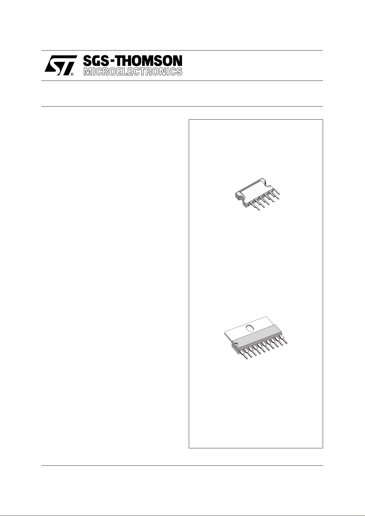
CLIPWATT 11
(Plastic Package)
ORDER CODE : STV9303W
DESCRIPTION
The STV9303 is a pulse driven vertical booster
intended for use in color TV. It includes a vertical
ramp generator specially designed to fit with deflection processors like STV2102 or STV2110 which
provide a 10.5 line lengh vertical pulse. The discharging of the sawtooth capacitor is triggerr ed by
the trailing edge of the vertical sync and the charging by the leading edge.
During the sync pulse duration, the sawtooth will
remains at its bottom value. Another possibility is
to use the internal monostable (by connecting an
external capacitor on Pin 5) to define the point
where the sawtooth will restart. Thi s second poss ibility is very usefull to avoid interlacing problems
when using a conventional deflection processor
delivering a small duration vertical pulse.
The STV9303 includes a very efficient power amplifier for direct driving of a TV picture tube in B &
W or color television.
For power consumption saving, a flyback generat or
is also included. The current and voltage capabilities (2.5App max output current and 70V flyback
peak voltage), make this IC also suitable for large
screen TV sets.
Thermal protection is also provided.
SIP10
(Plastic Package)
ORDER CODE : STV9303
September 1993
This is advance information on a new product now in development or undergoing evaluation. Details are subject to change without notice.
1/6
Page 2
STV9303
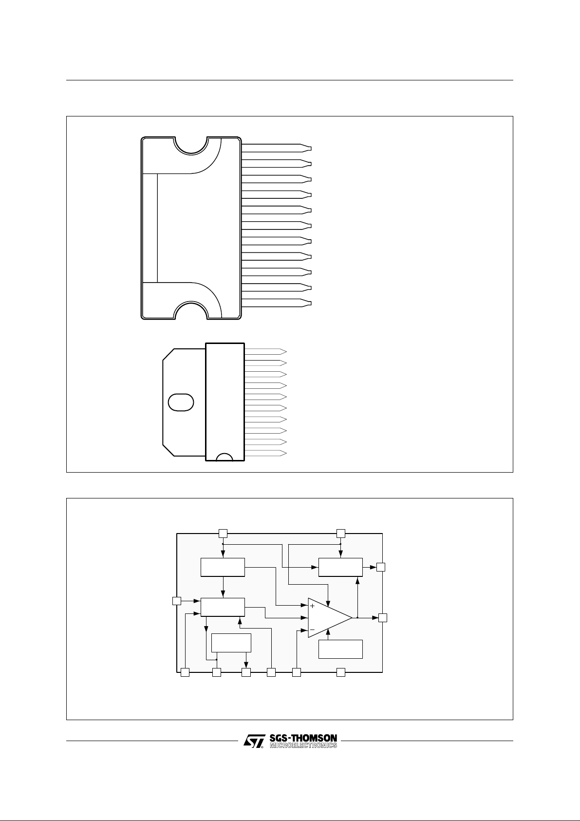
PIN CONNECTIONS
CLIPWATT11
11
10
FLYBACK GENERATOR
SUPPLY VOLTAGE
9
8
7
6
5
4
3
2
1
INVERTING INPUT
BUFFER OUTPUT
RAMP GENERATOR
GROUND
MONOSTABLE CAPACITOR
HEIGHT ADJUSTMENT
TRIGGER INPUT
OUTPUT STAGE POWER SUPPLY
POWER OUTPUT
SIP10
10
9
8
7
6
5
4
3
2
1
FLYBACK GENERATOR
SUPPLY VOLTAGE
INVERTING INPUT
BUFFER OUTPUT
RAMP GENERATOR
GROUND
HEIGHT ADJUSTMENT
TRIGGER INPUT
OUTPUT STAGE POWER SUPPLY
POWER OUTPUT
9303V-02.EPS/9303V-01.EPS
BLOCK DIAG RAM (CLI PW AT T)
SYNC
3
INPUT
SAWTOOTH
HEIGHT
2/6
V
S
10
VOLTAGE
REGULATOR
RAMP
GENERATOR
BUFFER
STAGE
SAWTOOTH
CAPACITOR
V
S
OUTPUT
STAGE
2
FLYBACK
GENERATOR
CLOCK
PULSE
5
MONO.
OUTPUT
CAPACITOR
SAWTOOTH
94
INVERTING
INPUT
POWER
AMP
THERMAL
PROTECTION
67 8
GROUND
FLYBACK
11
GENERATOR
POWER
1
OUTPUT
9303V-03.EPS
Page 3

STV9303
ABSOLUTE MAXIMUM RATINGS (CLIPW ATT Pin Connect i ons)
Symbol Parameter PIns Value Unit
V
S
, V
V
F
V
I-
I
OP
I
11
I
11
V
3
T
stg
T
THERMAL D ATA
Supply Voltage 10 35 V
Flyback Voltage 1-2 70 V
O
Amplifier Input Voltage 9 V
S
Peak Output Current 1 1.5 A
Flyback DC Current at VO < V
Flyback Peak Current (f = 50 or 60Hz, T
S
< 1.5ms) 11 1.8 A
fly
Trigger Input Voltage 3 V
11 100 mA
S
Storage Temperature -40, +150
Junction Temperature Internally limited
j
V
V
o
C
9303V-01.TBL
Symbol Parameter Value Unit
Junction Temperature at Thermal Shutdown Typ. 140
Thermal Protection Hysteresis Typ. 25
Junction-case Thermal Resistance CLIPWAT11
SIP10
Max.
Max.
3
10
R
T
pt
T
ph
th (j-c)
ELECTRICAL CHARACTERISTICS (CLIPWATT Pin Connections)
(V
= 35V, T
S
Symbol Parameter Test Conditions Min. Typ. Max. Unit
I
2
I
10
-I
7
-I
7
dI
7/I7
V
1L
V
1H
V
4
dV
4/VS
dV
4/dI4
V
R
V
D11-10
V
D1-2
G
V
V
fs
V
11
V
3
V
8
I
1
V
7M
I
7
K1 Delay between end of Sync Pulse and beginning
t
do
= 25oC, unless otherwise specified)
amb
Pin 2 Quiescent Current I1 = 0, I11 = 0 16 36 mA
Pin 10 Quiescent Current I1 = 0, I11 = 0 15 30 mA
Ramp Generator Bias Current V7 = 0 1 µA
Ramp Generator Current V7 = 0, -I4 = 20µA 18.5 20 21.5 µA
Ramp Generator Linearity V7 = 0 to 12V, -I4 = 20µA 0.2 1 %
Out Saturation Voltage to GND I1 = 0.1A
I1 = 1.25A
Out Saturation Voltage to V
S
-I1 = 0.1A
-I1 = 1.25A
0.1
1.212.0
0.9
1.6
1.6
3.0
Reference Voltage -I4 = 20µA 6.3 6.6 6.9 V
Reference Voltage Drift versus V
Reference Voltage Drift versus I
S
4
VS = 10V to 35V 1 2 mV/V
I4 = 10µA to 30µA 0.1 1 mV/µA
Internal Reference Voltage 4.15 4.40 4.65 V
Diode Fwd Voltage ID = 1.25A 1.5 3 V
Diode Fwd Voltage ID = 1.25A 1.5 3 V
Output Stage Open Loop Gain f = 100Hz 70 dB
V10-11 Saturation Voltage -I11 = 1.25A 1.5 3.0 V
Pin 11 Saturation Voltage I11 = 20mA 0.8 2 V
Trigger Input Threshold 2.6 3.0 3.4 V
Sawtooth Pedestall Voltage 1.85 V
Peak-to-peak Operating Current Range 0.4 2.5 A
Max. Voltage on Pin 7 12 V
Min. Discharging Current 5 mA
100 µs/nF
of Sawtooth versus value of Capacitor on Pin 5
Max. Delay between end of Sync Pulse and
210µs
beginning of Sawtooth Capacitor charging
without Capacitor on Pin 5
o
C/W
o
C/W
o
C
o
C
9303V-02.TBL
V
V
V
V
9303V-03.TBL
3/6
Page 4

STV9303
W AVEFO RMS
Sync Pulse (Pin 3)
Vertical Sawtooth on Pin 7 (Pin 5 NC with CLIPWATT or with SIP10)
t
do
Vertical Sawtooth on Pin 7 with Cd connected on Pin 5 (CLIPWATT only)
t
= (K1 . Cd) +
d
APPLICATION CIRCUIT (CLIPWA TT)
0.1µF
10
VOLTAGE
REGULATOR
TRIG. INP
180k
3
4
Ω
RAMP
GENERATOR
BUFFER
STAGE
7 8
t
1000µF
35V
CLOCK
PULSE
5
*
do
9303V-04.EPS
V
= 30V
S
1N4001
2
100µF
35V
FLYBACK
GENERATOR
POWER
AMP
THERMAL
PROTECTION
9
6
11
1
1.5Ω 330Ω
YOKE
Ry = 12.5
Ly = 25mH
Iy = 1.6App
Ω
YOKE
0.22µF
2.7kΩ
100µF
25V
1000µF
25V
4/6
220kΩ
820kΩ
100nF
100nF
100kΩ
56kΩ
8.2kΩ
2.2kΩ
Cd optional to adjust sawtooth start delay
*
2.7kΩ
1Ω
9303V-05.EPS
Page 5

PACKAGE MECHANICAL DATA
11 PINS - PLASTIC CL IPWATT
STV9303
C
A
H3
H1
L2
B
L
L1
D
E
M1
M
Dimensions
A 3.10 0.122
B 1.10 0.04
C 0.15 0.006
D 1.50 0.059
E 0.52 0.02
F 0.80 0.03
G 1.70 0.066
G1 17 0.66
H1 12.00 0.48
H3 20.00 0.79
L 17.90 0.70
L1 14.40 0.57
L2 11.00 0.43
M 2.54 0.1
M1 2.54 0.1
Min. Typ. Max. Min. Typ. Max.
Millimeters Inches
F
G1
G
PM-CPW11.EPS
CPW11.TBL
5/6
Page 6

STV9303
PACKAGE MECHANICAL DATA
10 PINS - PLASTIC SIP
C
c2
A
c1
Dimensions
L2
D
L1
1 10
a1
L
e3
N
M
B
b1
b3
L3
d1
e
Millimeters Inches
Min. Typ. Max. Min. Typ. Max.
A 7.1 0.280
a1 2.7 3 0.106 0.118
B 24.8 0.976
b1 0.5 0.020
b3 0.85 1.6 0.033 0.063
C 3.3 0.130
c1 0.43 0.017
c2 1.32 0.052
D 23.7 0.933
d1 14.5 0.571
e 2.54 0.100
e3 22.86 0.900
L 3.1 0.122
L1 3 0.118
L2 17.6 0.693
L3 0.25 0.0 10
M 3.2 0.126
N 1 0.039
Information furnished i s believed to be accurate and rel iabl e. However, S GS-THOMSON Microel ectroni cs assumes no responsibil ity
for the consequences of use of such information nor for any infringement of patents or other rights of third parties which may result
from its use. No licence is granted by implication or otherwise under any patent or patent rights of SGS-THOMSON Microelectronics.
Specifications mentioned in this publication are subject to change without notice. This publication supersedes and replaces al l
information previously supplied. SGS-THOMSON Microelectronics products are not authorized for use as critical components in life
support devices or systems without express written approval of SGS-THOMSON Microelectronics.
PM-SIP10.EPS
SIP10.TB L
6/6
© 1994 SGS-THOMSON Microelectronics - All Rights Reserved
2
Purchase of I
2
C Patent. Rights to use these components in a I2C system, is granted provided that the system conforms to
I
Australia - Brazil - China - France - Germany - Hong Kong - Italy - Japan - Korea - Malaysia - Malta - Morocco
The Netherlands - Singapore - Spain - Sweden - Switzerland - Taiwan - Thailand - United Kingdom - U.S.A.
C Components of SGS-THOMSON Microelectronics, conveys a license under the Philips
2
C Standard Specifications as defined by Philips.
the I
SGS-THOMSON Microelectronics GROUP OF COMPANIES
 Loading...