

Page 1
MULTISTANDARDVIDEO AND SOUND IF SYSTEM
WITHAUDIO AND VIDEO SWITCHES
.
VIDEOPLLDEMODULATION
.
SOUNDPLLDEMODULATION
.
POSITIVEANDNEGATIVEMODULATION
.
AGC FOR BG AND L STANDARDS
.
AUDIO SWITCH
.
DC VOLUME CONTROL
.
VIDEOSWITCH
DESCRIPTION
TheSTV8224Bis a pictureandsoundIFprocessor
formultistandardapplicationwith very fewexternal
componentsand adjustments.
It provides the audio and video switches for one
SCART plug application.
AM sound demodulation is performed with the
STV8225add-on.
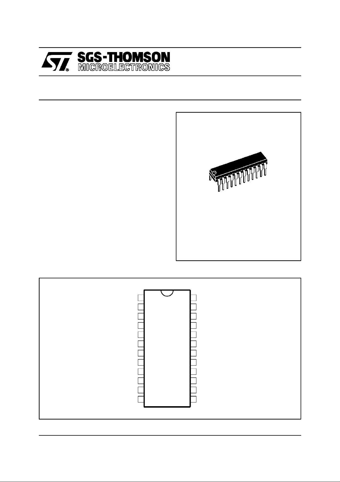
SHRINK24
(PlasticPackage)
ORDER CODE :
STV8224B
STV8224B
PIN CONNECTIONS
PIF PLL FILTER
AFC OUTPUT
CVBS OUTPUT
SWITCHINGINPUT (STANDARD + INT/EXT)
IF LC
IF LC
AUDIO HIGH PASS FILTER
2nd IF SOUND INPUT
AUDIO AND 2nd IF DECOUPLING
INTERNALVIDEO INPUT
VIDEO SWITCH OUTPUT
EXTERNAL VIDEO INPUT
January 1997
1
2
3
4
5
6
7
8
9
10
11
12
24
TUNER AGC STARTING POINT ADJUSTMENT
23
TUNER AGC OUTPUT
22
AGC CAPACITOR
21
AGC CAPACITOR (L STANDARD)
20
IF INPUT
19
IF INPUT
18
GROUND
17
V
CC
16
EXTERNAL AUDIO INPUT
15
FM DEMODULATEDAUDIO OUTPUT
14
AUDIO SWITCH OUTPUT
13
VOLUME CONTROL + MUTE
8224B -01.EPS
1/12
Page 2
STV8224B
BLOCKDIAGRAM
AFC
OUTPUT
PIF PLL
& AFC
EXT
CVBS
6dB
V
CC
1817125162
SWITCHED
11
CVBS
10
IF INPUT
TUNER
AGC
OUTPUT
19
20
21
AGC
22
23
TUNER
AGC
24
SWITCHED
DC
VOLUME
MUTE
14 13 15 7
AUDIO
VID
AMP
16
EXT
AUDIO
AUDIO
OUT
Int/Ext
BG/L
SIF
PLL
WHITE NOISE
&
SPOT INVERT
LOGIC
INTERFACE
LIMITER
AUDIO
Vref
STV8224B
3
SFE
5.5
4
8
9
SFE
6.5
ABSOLUTE MAXIMUMRATINGS
Symbol Parameter Value Unit
V
S
Vx Tuner AGC Voltage V
T
stg
T
oper
Supply Voltage 13.5 V
CC
Storage Temperature -40, +150
Operating Temperature 0, +70
CVBS
OUT
V
o
C
o
C
8224B -02.EPS
8224B-01.TBL
THERMAL DATA
Symbol Parameter Value Unit
Junction-ambient Thermal Resistance Max. 75
2/12
R
th (j-a)
o
C/W
8224B-02.TBL
Page 3
STV8224B
ELECTRICAL CHARACTERISTICS
(T
=25°C, VCC= 9V,IFinput= 10mV
amb
VideomodulationDSB,D = 90%at B/G,D = 95%at L,f
VideoBW= 5MHz,Soundcarrier input: 5.5MHz,10mV
Volumeattenuation= 0dB,unlessotherwisespecified)
Symbol Parameter Test Conditions Min. Typ. Max. Unit
SUPPLY
V
I
CC
IF AMPLIFIER
V
19-20
R
19-20
C
19-20
Gr Gain Control Range 68 dB
SYNCHRONOUS VIDEO DEMODULATOR
DF
AFC
S2 AFC Slope See Figure 21 0.2 µA/kHz
DEMODULATED VIDEO OUTPUT (Pin 3)
V
BG vs L Amplitude Difference 10 %
V
BW Bandwidth -3dB Video Signal 7 9 MHz
Dg Differential Gain 6 8 %
Dp Differential Phase 3 6 Degree
Vr3c Residual Carrier Signal (RMS Value) 1 10 mV
Vr3h Residual 2nd Harmonic (RMS Value) 1 10 mV
S/N Signal to Noise Ratio Note 1 - Weighted CCIR-567 56 61 dB
V
WTH
V
V
BTH
V
AGC CIRCUIT (BG MODE)
I
22CBG
I
22DBG
C/D Charging/Discharging Ratio 45
Notes :
Supply Voltage 8 9 12.6 V
CC
Supply Current I17,VCC=9V 70 95 mA
Input Sensitivity (RMS) -3dB Video at Output 70 µV
Differential Input Resistance 2 kΩ
Differential Input Capacitance 2 pF
Max Input Signal +1dB Video at Output 180 mV
Vision Carrier Capture -1.4 1.6 MHz
PC
Amplitude TopSync to White 2 2.3 2.6 V
A3
Top Sync Level B/G and L 1.6 1.9 2.2 V
S3
Zero Carrier Level B/G
Internal Bias of Emitter Follower 3 5 mA
I
3
Intermodulation 1.07MHz Note 2 52 dB
White Noise Threshold Voltage 4.85 V
White Noise Insertion Level 3.6 V
WIL
Black Noise Threshold Voltage 1.3 V
Black Noise Insertion Level 2.5 V
BIL
Charging Current 550 950 1300 µA
Discharge Current 12 20 28 µA
S
=
1.
20 log 10
N
2. Video carrier relative level = 0dB, Chroma subcarrier level = -3.2dB, Sound carrier relative level = -20dB.AGC voltage (Pin 22)
is adjustedto get 1V
V
out black white
(
V
mV
N
atBW = 5MHz
)
RMS
signalon output (Pin 3).
PP
synclevelat B/G, Peak-whitelevelat L,
RMS
=38.9MHz,fSC= 33.4MHz,
PC
RMS,fM
=1kHz,AudioBW= 20kHz,∆f=±50kHz,
L
4.4
1.8
RMS
RMS
PP
V
V
8224B-03.TBL
3/12
Page 4
STV8224B
ELECTRICAL CHARACTERISTICS
=25°C,VCC= 9V, IF input= 10mV
(T
amb
VideomodulationDSB,D = 90% atB/G,D = 95% at L, f
VideoBW=5MHz,Soundcarrierinput: 5.5MHz,10mV
(continued)
synclevelat B/G,Peak-whitelevelat L,
RMS
= 38.9MHz,fSC=33.4MHz,
PC
RMS,fM
=1kHz,AudioBW= 20kHz,∆f=±50kHz,
Volumeattenuation= 0dB, unlessotherwisespecified)
Symbol Parameter Test Conditions Min. Typ. Max. Unit
AGC CIRCUIT (L MODE)
I
22CL
I
22DL
I
22CL
I
22DL
TUNER AGC
I
23
S23 Current Slope R
I
23+
FM SOUND DEMODULATION
V
8S
R
AMR Amplitude Modulation Rejection Note 5 50 61 dB
SVR Supply Voltage Rejection Ratio Ripple signal : 100Hz, 0.5V
V
15
THD Total Harmonic Distortion 0.2 1 %
R
15
S/N Signal to Noise Ratio See Note 6,
Charging Current Note 3 2 3.3 4.5 mA
Discharge Current 0.3 µA
+ Additional Charging Current L in case of missing, VITS Pulses
5 µA
and no White in Video Content
Threshold Voltage Level for
Refered to Pin 3 2.75 V
Additional Charging Current
+ Additional Discharging Current 28 40 56 µA
Threshold Voltage Level for
Refered to Pin 3 2.25 V
Additional Discharging Current
Maximum Sinked Current 1.5 2 2.5 mA
=5kΩ 100 170 230 µA/dB
24
Maximum Tuner Plus Sinked
Note 4 40 mA
Current
Input Sensitivity 150 µV
Limiter Input Resistance 600 Ω
8
DC Voltage (Pin 8) 4.2 V
PP
28 33 dB
Detected AudioOutput Signal 0.85 1.1 1.4 V
Internal Deemphasis Resistor 600 750 900 Ω
55 60 dB
Weighted CCIR 468-4,
(quasi peak level) input Pin 8
Black Picture (sync only) Measurement between IF input
White Picture 46 50 dB
250kHz Square Wave 47 52 dB
(Pins19-20) and audiooutput(Pin 15)
SAW : K2955
BPF : SFE5.5MB
47 52 dB
RMS
RMS
VOLUME CONTROL
Range Control Range SeeFigure 22 72 77 dB
V
C
Notes : 3. Triggeredon white level
4. Additional sinked current forlarge increasing steps of input signal when:
- VoltagePin 22 > starting point defined Pin 24.
- Outputsignal (Pin 3) saturated(V
5. AMR = 20 log
S
6.
= 20 log
N
(mV
V
RMS
RMS
)
RMS
AM
)
(dB)
)
V
15
(mV
V
15
V
(mV
N
< V BTH inBG mode, V3> V WTH in L mode).
3
(dB) where VAM= output amplitude in AM for fM= 1kHz and m = 30%
4/12
8224B-04.TBL
Page 5

STV8224B
ELECTRICAL CHARACTERISTICS
=25°C, VCC= 9V,IFinput= 10mV
(T
amb
VideomodulationDSB,D = 90%at B/G,D =95% at L, f
VideoBW= 5MHz,Soundcarrier input: 5.5MHz,10mV
(continued)
synclevelat B/G,Peak-whitelevelat L,
RMS
=38.9MHz, fSC= 33.4MHz,
PC
RMS,fM
=1kHz,AudioBW = 20kHz,∆f=±50kHz,
Volumeattenuation= 0dB, unlessotherwisespecified)
Symbol Parameter Test Conditions Min. Typ. Max. Unit
AUDIO SWITCH
R
16
CRtk Crosstalk 70 80 dB
En Output Noise Level (Pin 14) Weighted CCIR 468-4,V
EXTHD THD onExternal Signal (Pin 14) V
VIDEO SWITCH
V
DC 12
V
S12
V
11
V
S11
GEX Gain from Ext. Input to Output 5.5 6 6.5 dB
I
12
VBW Bandwidth V
G
IN
MUTE (Pin13)
V
TH13
CONTROL INPUT
Input Resistance 55 70 85 kΩ
(quasi peak level)
IN
=2V
, Attenuation = 0dB 0.1 0.3 %
RMS
13
= 0.5V
70 µV
Audio Reference Voltage (Pin 9) 4.5 V
DC Input Level No signal 1.6 1.9 2.2 V
Top Sync. Clamp Level 1.8 V
DC Output Level No signal 1.7 2 2.3 V
Top Sync. Clamp Level 1.5 V
Crosstalk 55 dB
Output Swing 4 5 V
Input Current V12=V
=1V
IN
= 1.5V 1 5 µA
DC12
PP
15 MHz
Gain from Int. Input to Output -0.5 0 +0.5 dB
Threshold Voltage Pin 13 0.2 0.3 0.4 V
Negative Modulation Video : External - Audio : External 7.2 V
Threshold 3 Level linked to V
CC
6.4 6.8 7.2 V
Positive Modulation Video : External - Audio : External 4.9 6.4 V
Threshold 2 Level linked to V
CC
4.1 4.5 4.9 V
Positive Modulation Video : Internal - Audio : External 2.6 4.1 V
Threshold 1 Level linked to V
CC
1.8 2.2 2.6 V
Negative Modulation Video : Internal - Audio : Internal 1.8 V
8224B-05.TBL
5/12
Page 6

STV8224B
INPUT/OUTPUT PIN CONFIGURATION
Figure1 : PIFPLL Filter
1
Figure 2 : AFCOutput
2
8224B -03.EPS
Figure3 : CVBS Output
3
Figure5 :
56
IFLC
2kΩ 2kΩ
Figure 4 : SwitchingInput Standard+ INT/EXT
4
8224B-05.EPS
Figure 6 :
Audio High Pass Filter
7
8224B-04.EPS
8224B -06.EPS
6/12
8224B-07.EPS
8224B-08.EPS
Page 7

INPUT/OUTPUT PIN CONFIGURATION (continued)
Figure7 : 2ndIF Sound Input (Pin 8)
Audio and 2
nd
IF Decoupling (Pin 9)
STV8224B
Figure 8 : InternalVideoInput
8
Figure9 :
Figure11 :
Ω
600Ω
600
VideoSwitch Output
11
VolumeControl + Mute
9
10
8224B-09.EPS
Figure 10 :
8224B-11.EPS
Figure 12 :
ExternalVideo Input
12
AudioSwitch Output
8224B-10.EPS
8224B-12.EPS
13
Figure13 : FM DemodulatedAudio Output
750
Ω
15
14
8224B-13.EPS
Figure 14 : ExternalAudio Input
16
8224B-15.EPS
8224B-14.EPS
8224B-16.EPS
7/12
Page 8

STV8224B
INPUT/OUTPUT PIN CONFIGURATION (continued)
Figure15 : V
CC
Figure 16 : IF Input
Figure17 :
21
17
AGC Capacitor
15V
8224B -17.EPS
Figure 18 :
19
AGCCapacitor
22
1kΩ
1kΩ
20
8224B -18.EPS
Figure19 :
8/12
TunerAGC Output
23
8224B-19.EPS
Figure 20 :
8224B-21.EPS
8224B-20.EPS
TunerAGC Starting Point Adjustment
24
8224B-22.EPS
Page 9

STV8224B
Figure21 : AFC Voltage Pin 2 vs IF Frequency
8
7
6
5
4
3
2
1
AFCVOLTAGE (PIN 2) (V)
0
38.55 38.95 39.3538.75 39.15
IF FREQUENCY(MHz)
Figure23 :
TunerAGC Output Current vs V
CurrentConversion
with 100kΩ/100kΩ Bridge
IN
(R24 is external adjustmentPin 24)
2
1.75
1.5
1.25
1
0.75
0.5
0.25
0
-1
10
TUNER AGC OUTPUT CURRENT (mA)
Figure 25 :
R24 = 1kΩ
R24 = 3kΩ
R24 = 5kΩ
11010
V (mV )
RMS
IN
2
Blackand White Noise Inverter
10
Figure 22 : Volume Control Attenuationvs V
0
-10
-20
-30
-40
-50
-60
ATTENUATION(dB)
VOLUME CONTROL
-70
-80
1.0 2.0 3.0
V (V)
8224B-23.EPS
Figure24 :
Video Signal to Noise Ratio (Pin 3)
13
as a functionof IF InputSignal
(Pins 19-20) WeightedCCIR-567
80
70
60
50
40
S/N (dB)
30
20
10
3
8224B -25.EPS
0
VIN(mV
RMS
13
4.0
)
5.0
8224B-24.EPS
1001010.10.01
8224B -30.EPS
4.85
4.2
3.6
2.5
1.9
1.3
V
(V)
3
White Spike Noise Clamp
Top White
White Noise Level Insertion
Black Noise Level Insertion
Top Synchronization
Black Spike Noise Clamp
t
8224B-26.EPS
9/12
Page 10

STV8224B
APPLICATIONDIAGRAM(B/G/D/K)
STV8224B
External
Sound
C9
Input
10µF
(From SCART)
C8
R11
Demodulated
Sound
Output
(To SCART)
10µF
220Ω
Sound
Switched
C6
Output
R32
4.7µF
C7
3.3kΩ
10kΩ
68nF
+9V
P2
Volume control
CVBS
Output
Q2
BC547
R18
R12
2.2kΩ
TRAP FILTER
(5.5MHz - 6.5MHz)
(To SCART)
75Ω
R9
560Ω
L6
CF3
8.2µH
CVBS
CVBS
Input
(From SCART)
10kΩ
C31
100nF
SW1
Mute
1314
External
C30
R29
470nF
Ouput
75Ω
R10
22Ω
+9V
C27
470nF
SW4
+9V
R28
4.7kΩ
Q3
BC547
STD
R26
3.9kΩ
C24
1nF
C29
10V
BZX55C
10nF
R24
4.7kΩ
R21
C26
AGC
Q4
LC1
123456789101112
Delay
9V
C33
BC337
C25
C15
100nF
10µF
100nF
1nF
10µF
R13
DZ1
38.9MHz
330Ω
1617181920 1521222324
C21
L4
3.3µH
BGDK
FILTER
VIDEO SAW
IF1
C20
47µF
100nF
STV8224B
1µF
C18
10kΩ
P1
Tuner
C17
10nF
27kΩ
R14
1.8kΩ
D2
CF1
BFP
5.5MHz
C28
Voltage
Switching
C32
10nF
R25
2.7kΩ
R20
1kΩ
1N4148
68pF
BFP
D1
CF2
6.5MHz
R27
1N4148
1.8kΩ
R22
150Ω
10/12
Tuner AGC
C16
Output
R35
15Ω
R34
2.2µF
R15
6.8kΩ
12V
390Ω
100kΩ
AFC
R16
Output
100kΩ
8224B-27.EPS
R17
9V
Page 11

APPLICATIONDIAGRAM(B/G/D/K,L)
STV8224B- STV8225
External
Sound
Input
(From SCART)
Sound
Output
(To SCART)
C9
C8
10µF
R11
10µF
220Ω
C22
C23
10µF
10µF
891011121314
Sound
Switched
C6
Output
R32
4.7µF
C7
10kΩ
68nF
STV8224B
+9V
3.3kΩ
P2
10kΩ
Volume Control
C31
1314
100nF
SW1
Mute
CVBS
External
C30
Input
(From SCART)
R29
470nF
CVBS
Ouput
75Ω
R10
+9V
C27
470nF
SW4
STD
R26
BC547
+9V
R28
4.7kΩ
Q3
CVBS
Output
(to SCART)
Ω
75
R18
22Ω
Q2
R9
R12
2.2kΩ
TRAP FILTER
(5.5MHz - 6.5MHz)
560Ω
CF3
L6
8.2µH
BC547
3.9kΩ
C11
L7
D2
CF1
5.5MHz
C28
R16
Output
R25
2.7kΩ
1.8kΩ
R20
1kΩ
1N4148
BFP
6.5MHz
68pF
Voltage
Switching
Ω
100k
D1
CF2
R27
1N4148
Ω
1.8k
R22
150Ω
8224B-28.EPS
C24
1nF
38.9MHz
C29
330Ω
BZX55C
10V
9V
10nF
R17
R24
100kΩ
C32
4.7kΩ
R21
BFP
10nF
AFC
C26
AGC
Q4
R35
12V
123456789101112
Delay
9V
BC337
15Ω
LC1
C33
C25
C15
10µF
100nF
10µF
100nF
1nF
R34
R13
DZ1
390Ω
C20
C19
C18
Tuner AGC
100nF
47nF
1µF
C17
R14
C16
Output
P1
10nF
27kΩ
47µF
1617181920 1521222324
10kΩ
IC2 STV8224B
Tuner
R15
6.8kΩ
Level
C12
47µF
3.3µH
100nF
C10
22µF
SOUND SAW
L STD
FILTER
IF2
IC1 STV8225
Switch
C21
47µF
C13
10µF
1234567
L4
3.3µH
BGDKL
FILTER
VIDEO SAW
IF1
11/12
Page 12

STV8224B
PACKAGE MECHANICAL DATA
24 PINS - PLASTICSHRINK DIP
BeB1
E
E1
A2
A1
LA
Stand-off
c
D
e1
e2
E
13
F
12
SDIP24
e3
e2
.015
0,38
Gage Plane
Dimensions
24
1
Millimeters Inches
Min. Typ. Max. Min. Typ. Max.
A 5.08 0.20
A1 0.51 0.020
3.05 3.30 4.57 0.120 0.130 0.180
B 0.36 0.46 0.56 0.0142 0.0181 0.0220
B1 0.76 1.02 1.14 0.030 0.040 0.045
C 0.23 0.25 0.38 0.0090 0.0098 0.0150
D 22.61 22.86 23.11 0.890 0.90 0.910
E 7.62 8.64 0.30 0.340
E1 6.10 6.40 6.86 0.240 0.252 0270
e 1.778 0.070
e1 7.62 0.30
e2 10.92 0.430
e3 1.52 0.060
L 2.54 3.30 3.81 0.10 0.130 0.150
Informationfurnishedisbelieved to be accurate and reliable.However,SGS-THOMSON Microelectronics assumesno responsibility
for theconsequences of use of such information nor for any infringement of patentsor other rights of third parties which may result
from its use.Nolicence is grantedbyimplication orotherwise underany patent or patent rights of SGS-THOMSON Microelectronics.
Specifications mentioned in this publication are subject to change without notice. This publication supersedes and replaces all
informationpreviouslysupplied. SGS-THOMSONMicroelectronicsproducts arenotauthorized for use as criticalcomponents in life
support devices or systems without express written approval of SGS-THOMSON Microelectronics.
PMSDIP24.EPS
SDIP24.TB L
12/12
1997 SGS-THOMSONMicroelectronics - AllRights Reserved
Purchase of I2C Components of SGS-THOMSON Microelectronics, conveys a license under the Philips
2
C Patent. Rights to use these components in a I2C system, is granted provided that the system conforms to
I
2
the I
C Standard Specifications as defined by Philips.
SGS-THOMSON Microelectronics GROUP OF COMPANIES
Australia - Brazil - Canada - China - France - Germany - HongKong - Italy - Japan - Korea - Malaysia - Malta - Morocco
The Netherlands - Singapore-Spain - Sweden- Switzerland - Taiwan - Thailand - United Kingdom - U.S.A.
 Loading...