

Page 1
.
VERYLOWCURRENT ABSORPTION
.
3 STAGEIF GAIN CONTROLLEDAMPLIFIER
.
SYNCHRONOUS VIDEO DEMODULATOR
.
WHITESPOTANDNOISEINVERTER
.
AGCCIRCUIT WITH NOISEGATING
.
TUNERAGC OUTPUTFORPNPTUNERS
.
FM DETECTOR
.
AF AMPLIFIER WITH DC VOLUME CONTROL
.
AFC
.
2VPPONVIDEOOUTPUT
DESCRIPTION
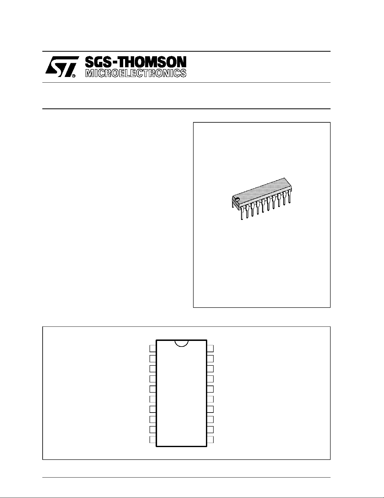
The STV8211is a monolithic integrated circuit in
DIP20 package for black& whitetelevision receivers usingPNP tuners. It is intendedtooperatewith
a negatively modulated vision carrier and frequency modulated sound carrier. Used with
TEA2037A(H/V deflectioncircuit), this IC permits
a complete low-cost solution for black and white
applications.
STV8211
VIDEO & SOUND IF SYSTEM
ADVANCE DATA
DIP20
(Plastic Package)
ORDER CODE : STV8211
PIN CONNECTIONS
CC
1
2
3
4
5
6
7
8
9
10
TUNER DELAY RESISTOR
TUNER OUTPUT CURRENT
V
NOT TO BE CONNECTED
IF INPUT
IF INPUT
GROUND
AUDIO OUTPUT
SOUND VOLUME CONTROL
FM TANK LC
August 1994
This isadvance informationon a new product now in developmentor undergoingevaluation. Detailsare subjectto change withoutnotice.
20
AGC MEMORY CAPACITOR
19
IF LC
18
IF LC
17
VIDEO PEAKING
16
AFC TANK LC
15
AFC OUTPUT
14
CVBS OUTPUT
13
NOT TO BE CONNECTED
12
2nd IF SOUND CHANNEL INPUT
11
2nd IF SOUND CHANNEL INPUT
8211-01.EPS
1/8
Page 2
STV8211
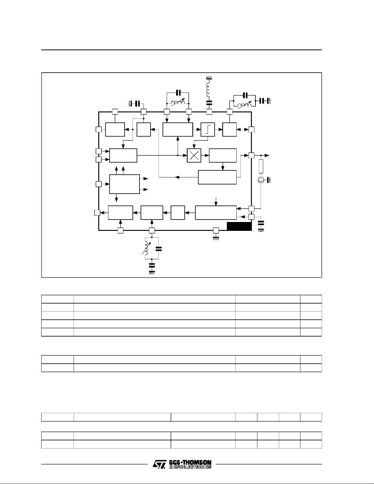
BLOCK DIAGRAM
I TUNER OUT
IF INPUT
IF INPUT
V9V
CC
AUDIO OUTPUT
2
5
6
3
8
RTD
1
TUNER
DELAY
3IF
AMPLIFIER
BAND GAP
REFERENCE
VOLTAGE
VOLUME
CONTROL
910
5.5MHz
AGC
DICRETE
FM
38.9MHz
REFERENCE
AMPLIFIER
LPF
Video
Peaking
1617181920
AFC
VIDEO
AMPLIFIER
WHITE & NOISE
SPOT INVERTER
4 STAGE LIMITER
STV8211
7
38.9MHz
15
AFC OUTPUT
14
12
11
CVBS OUTPUT
5.5MHz
ABSOLUTEMAXIMUM RATINGS
Symbol Parameter Value Unit
V
S
V
X
P Power Dissipation at T
T
stg
Supply Voltage 13.5 V
Tuner AGC Voltage V
=70oC 880 mW
amb
S
Storage Temperature - 40, + 150
THERMALDATA
Symbol Parameter Value Unit
R
th(j-a)
Junction-ambient Thermal Resistance Max. 80
ELECTRICAL CHARACTERISTICS
=25oC, VCC=9V, IF input = 10mV
(T
amb
Soundcarrierinput : 5.5MHz,10mV
RMS,fm
topsync,D = 90%, VideoBW= 5MHz,
RMS
=1kHz,Audio BW = 20kHz, ∆f=±25kHz,
Volumeattenuation= 0dB, unless otherwisespecified)
Symbol Parameter Test conditions Min. Typ. Max. Unit
SUPPLY
Supply Voltage 8 9 12.8 V
Supply Current 14 20 28 mA
o
o
C/W
8211-02.EPS
V
C
8211-01.TBL
8211-02.TBL
8211-03.TBL
2/8
Page 3
STV8211
ELECTRICAL CHARACTERISTICS
=25oC, VCC=9V,IF input = 10mV
(T
amb
Soundcarrierinput : 5.5MHz,10mV
RMS,fm
Volumeattenuation= 0dB, unless otherwisespecified)
Symbol Parameter Test conditions Min. Typ. Max. Unit
IF AMPLIFIER
AGC Range 58 64 67 dB
IF - Sensitivity (RMS) Video out -3dB 70 µ
R Input Differential
C Input Stray 2pF
DEMODULATED VIDEO OUTPUT
S/N Video (BW = 5MHz) IF inp. = 10mV
Intermodulation 1.07MHz AGC open loop, Picture carrier = 0dB,
Detected Video Output
Peak-to-peak (positive)
TopSynchro Output Level 1.9 V
Video Bandwidth with Output Filter -3dB, see Figures 1 and 2 7 MHz
Differential Phase 3 7 Degree
Differential Gain 37 %
White Noise Clamp
White Noise Insertion 3.2 V
Video Output Current Capability 1.2 2 2.6 mA
Residual Output Carrier (RMS) At 38.9MHz
AFC
AFC Slope
AGC CIRCUIT
Maximum I Charge 550 900 1200 µ
Maximum I Discharge 14 20 26 µ
I
CH /IDISCH
TUNER AGC
Sinked Current Suitable for Mosfet-NCH 1.15 2 2.6 mA
Slope
DEMODULATED AUDIO OUTPUT
Detected Output Audio Signal (RMS) 120 270 350 mV
TotalHarmonic Distorsion 0.5 2 %
Amplitude ModulationRejection m = 30% 40 53 dB
2nd IF Sound Sensitivity -3dB FM
Detected Audio Signal (RMS)
S + N
N
Thermal Drift of Volume 0.05
Input Resistance Limiter 400 560 720 Ω
VolumeControl versus V
Ratio 45 -
9
top sync, D =90%, VideoBW = 5MHz,
RMS
=1kHz,AudioBW = 20kHz,∆f=±25kHz,
Guaranteed by process
V
9
V
9
(WH− BL)
10
= 2.5V
= 0.9V
N
RMS
, 20 log
RMS
Chrominance carrier = -3.2dB,
Sound carrier = -20dB
Referred to the video output
see Figure6
At 77.8MHz
With R
= 200kΩ, see Figure 3
Load
RTD = 0 ÷ 10kΩ
∆f=±25kHz for signal
∆f= 0 after deemphasis (BW = 20kHz)l
See Figure4 V9= 4.5V
1 1.5 2
49 55 dB
50 dB
1.8 2 2.4 V
4.5 V
1020mV
25 40 60 mV/kHz
600
µA/dB
200
50 60 dB
0
12
187424
65
kΩ
mV
µV
dB
o
dB
dB
dB
V
A
A
C
8211-04.TBL
3/8
Page 4

STV8211
TEST CIRCUIT
VIF Input
38.9MHz
M = 100%
R = 10%
AMDSB
10nF
4
4
10nF
10µF
100nF
5
200Ω
6
7
9V
DC
10µH
IoT V1TUN
ABC
Ω
100
10kΩ
1µF
123
100nF
SW1
1.8kΩ
47pF
STV8211
9V
220Ω
Q=80
38.9MHz
181920
6.2 V
2.2kΩ
180Ω
16
15
14
12
Z
38.9MHz
Q=80
47pF
470nF
10nF
9V
100kΩ100kΩ
D AFCOutput
E
Video Out1
L AudioSignal
withoutDeemphasis
8910
1kΩ
47nF
I AudioOutput
withDeemphasis
4.7kΩ
Volume
Control
Figure 1 : Output Signal Bandwidth without
Video peaking
V (dB)
OUT
0
-3
-6
-9
-12
-15
0246810
17
27pF
4.7µH
F (MHz)
100pF
100nF
5.5MHz
Q>40
33nF
11
100nF
50Ω
FM Input
Figure2 : OutputSignalBandwidthwith
Video peaking
V (dB)
OUT
0
-3
-6
-9
-12
-15
8211-04.EPS
0246810
E Video Out 2
8211-03.EPS
F (MHz)
8211-05.EPS
4/8
Page 5

STV8211
Figure 3 : AFC VoltageversusInput Frequency
Figure4 : Volume ControlAttenuationversus
Voltagein Pin 9
AFC OUTPUT
VOLTAGE (V)
8
6
4
2
0
38.5 39.338.7 38.9 39.1
IF FREQUENCY
(MHz)
-20
-40
-60
-80
-100
ATTENUATION
8211-06.EPS
(V)
123450
Figure 5 : Typical ConnectionfromµPto STV8211for Remote Volume Control (Pin9)
Processor
Pushpull
Output
10k
Ω
STV8211
9
V (V)
9
8211-07.EPS
ST63XX
Figure 6 : Blackand White Noise Inverter
V (V)
14
4.5
3.9
3.2
2.5
1.9
1.3
80k
C
Ω
8211-08.EPS
White spike noise clamp
Top white
White noise level insertion
Noise level insertion
Top synchronization
Black spikes noise clamp
t(s)µ
8211-09.EPS
5/8
Page 6

STV8211
Figure 7 : TypicalApplication
10nF27pF
Ω
AFC
Output
200k
S
V
47pF
Q=80
38.9MHz
16
15
4.7µH
Video
Output
µF
1
200kΩ
56pF
15µH
1kΩ
14
Tuner AGC OUT
Q=80
38.9MHz
µH
10
100nF
F
µ
10
Ω
100
µH
10
47pF
Ω
3.9k
10µF
100nF 100nF
1µF
10kΩ
9.1V
H
µ
1
Ω
1.8k
1819 17
120
23
55
1
1nF
STV8211
6
4
OFW
G1959
2
560Ω
7
3
BF959
12
11
109
8
560Ω
Ω
1.2k
10nF
Ω
100
Q>40
4.7kΩ 1kΩ 10kΩ
100pF
5.5MHz
BPF
47nF
100nF
33nF
DC
Audio
Control
Volume
Output
5.5MHz
6/8
S
V = 12V
Ω
1nF
51Ω
IF
IN
8211-10.EPS
3.3k
10µF
Page 7

Figure 8 : PCBoard and Components Lay-out of the Circuit of Figure7 (1 : 1 scale)
STV8211
8211-11A.TIF/8211-11B.TIF
7/8
Page 8

STV8211
PACKAGE MECHANICAL DATA
20 PINS- PLASTIC DIP
Dimensions
Min. Typ. Max. Min. Typ. Max.
Millimeters Inches
a1 0.254 0.010
B 1.39 1.65 0.055 0.065
b 0.45 0.018
b1 0.25 0.010
D 25.4 1.000
E 8.5 0.335
e 2.54 0.100
e3 22.86 0.900
F 7.1 0.280
i 3.93 0.155
L 3.3 0.130
Z 1.34 0.053
Information furnished is believedto be accurate andreliable. However, SGS-THOMSON Microelectronics assumes no responsibility
for the consequences ofuse of such information norfor anyinfringement ofpatents or otherrights of third partieswhich may result
from itsuse. No licence isgranted by implication orotherwise under anypatent orpatent rights of SGS-THOMSON Microelectronics.
Specifications mentioned in this publication are subject to change without notice. This publication supersedes and replaces all
information previously supplied. SGS-THOMSONMicroelectronics products arenot authorized for use ascritical components in life
support devices or systems without express written approval of SGS-THOMSON Microelectronics.
1994 SGS-THOMSON Microelectronics - All Rights Reserved
Purchase of I
2
I
C Patent. Rights to use these components in aI2C system, is granted provided that thesystem conforms to
Australia - Brazil - China - France - Germany - Hong Kong - Italy - Japan - Korea - Malaysia - Malta - Morocco
The Netherlands - Singapore -Spain - Sweden - Switzerland - Taiwan - Thailand - United Kingdom - U.S.A.
2
C Components of SGS-THOMSON Microelectronics, conveys a license under the Philips
2
the I
C Standard Specifications as definedby Philips.
SGS-THOMSON Microelectronics GROUP OFCOMPANIES
PM-DIP20.WMF
DIP20.TBL
8/8
 Loading...