

Page 1
MULTISTANDARDTV SOUNDDEMODULATOR
.
PERFORMS FM MONO, FM 2 CARRIERS
ANDNICAMRECEPTION
.
B/D/G/H/I/K/K1/K2/L/L’
.
UPTO 500kHzDEVIATIONFM DEMODULA TOR
.
ALL PRE AND POST-PROCESSING INTEGRATEDFILTERS,ALIGNMENTFREE
.
STANDARDRECOGNITIONFLAG
.
SINGLEQUARTZ CRYSTAL
.
I2C BUSCONTROLLED
.
AMAND DOUBLESCARTAUDIO MATRIX
.
STAND-BYWITH THRU MODE
.
SINGLEBIT DACS
.
EASY IMPLEMENTATION OF AUTOSTANDARDMODE
.
ADVANCED OPERATING MODE FOR FULL
CUSTOMIZATION
.
SIFAGC WITHWIDE RANGE
STV8203
PRELIMINARY DATA
SHRINK42
(Plastic Package)
ORDER CODE : STV8203
DESCRIPTION
The STV8203provides all the necessary circuitry
for demodulationof all Nicamand Germanstereo
audiotransmission. It is very suitable forTV applicationsas well as for VCR, Personal Computer or
Set Top Box applications. Different transmission
standardsare automaticallydetectedand demodulated without user intervention. The recovered
audio signals can be made available in analog
form. More, the STV8203integrates an audio matrixwith a THRU modewhen the IC is in stand-by.
Very flexible applications are possible thanks to
smart I
appropriateaudio processingICs.
January 1999
This is advance information on a new product now in developmentor undergoing evaluation. Detailsare subject to change without notice.
2
C program modes and large choice of
TQFP44 (10 x 10 x 1.4mm)
(Full Plastic Quad Flat Pack)
ORDER CODE : STV8203D
1/31
Page 2
STV8203
SDIP42PIN CONNECTIONS
CAP5
SIF1
CAP6
SIF2
GND3
MOUT
MIN
CAP8
LIL1
LIR1
GND4
LIL2
LIR2
CAP2
CAP1
AOL1
AOR1
CAP4
AOL2
AOR2
1
2
3
4
5
6
7
8
9
10
11
12
13
14
15
16
17
18
19
20
21 22
CC
42 GND2
41
DV
DD5
REG
40
CAP3
39
NC
38
SCL
37
SDA
36
NOT USED
35
XIN
34
XOUT
33
GND1
32
NC
31
NC
30
NC
29
NC
28
NC
27
NC
26
NC
25
NC
24
RESET
23
CAP7AV
8203-01.EPS
TQFP44PIN CONNECTIONS
MOUT
MIN
CAP8
LIL1
LIR1
GND4
LIL2
LIR2
CAP2
CAP1
AOL1
2/31
GND3
SIF2
SIF1
CAP6
12
13
14
15
16
17
18
19
20
21
22
23 24 25 26 27 28 29 30 31 32 33
AOL2
CAP4
AOR1
AOR2
CAP5
NC
GND2
CC
AV
DD5
DV
CAP7
CAP3
REG
NC
RESET
NC
NC
NC
1234567891011
44
43
42
41
40
39
38
37
36
35
34
NC
SCL
SDA
NOT USED
XIN
XOUT
GND1
NC
NC
NC
NC
NC
8203-02.EPS
Page 3

PIN LIST
Pin Number
SDIP42 TQFP44
1 7 CAP5 Analog Decoupling for ADC SupplyRegulator Output
2 8 SIF1 Analog Subcarrier 1 Input
3 9 CAP6 Analog Decoupling for Input Amplifier Reference
4 10 SIF2 Analog Subcarrier 2 Input
5 11 GND3 Power Ground for Input Amplifier
6 12 MOUT Analog Mono Audio Output
7 13 MIN Analog Mono Audio Input
8 14 CAP8 Analog ADC VtopDecoupling
9 15 LIL1 Analog Line 1 Left Input (SCART 1)
10 16 LIR1 Analog Line 1 Right Input (SCART 1)
11 17 GND4 Power Audio Ground
12 18 LIL2 Analog Line 2 Left Input (SCART 2)
13 19 LIR2 Analog Line 2 Right Input (SCART 2)
14 20 CAP2 Analog Decoupling forAudio Matrix
15 21 CAP1 Analog Decoupling forBandgap Reference
16 22 AOL1 Analog Line 1 Left Output (SCART 1)
17 23 AOR1 Analog Line 1 Right Output (SCART 1)
18 24 CAP4 Analog Audio Matrix V
19 25 AOL2 Analog Line 2 Left Output (SCART 2)
20 26 AOR2 Analog Line 2 Right Output (SCART 2)
- 27 NC - Not Connected
21 28 AV
22 29 CAP7 Analog Decoupling forDigital Regulator Output
23 30 RESET Input Power On Reset
24 31 NC - Not Connected
25 32 NC - Not Connected
26 33 NC - Not Connected
27 34 NC - Not Connected
28 35 NC - Not Connected
29 36 NC - Not Connected
30 37 NC - Not Connected
31 38 NC - Not Connected
32 39 GND1 Power Digital Ground
33 40 XOUT Analog Crystal Oscillator Output
34 41 XIN Analog Crystal OscillatorInput
35 42 Not used Input To be connected to ground
36 43 SDA Bi-directional I
37 44 SCL Input I
- 1 NC - NotConnected
38 2 NC - Not Connected
39 3 CAP3 Analog Decoupling for Digital 3V (regulator output)
40 4 REG Analog Base Drive for External Regulator Transistor
41 5 DV
42 6 GND2 Power Digital Ground
Name Type Function
(5V)
DD
CC
DD5
Power Audio Matrix Supply
2
C SerialData
2
C SerialClock
Power 5V Supply
STV8203
8203-01.TBL
3/31
Page 4
STV8203
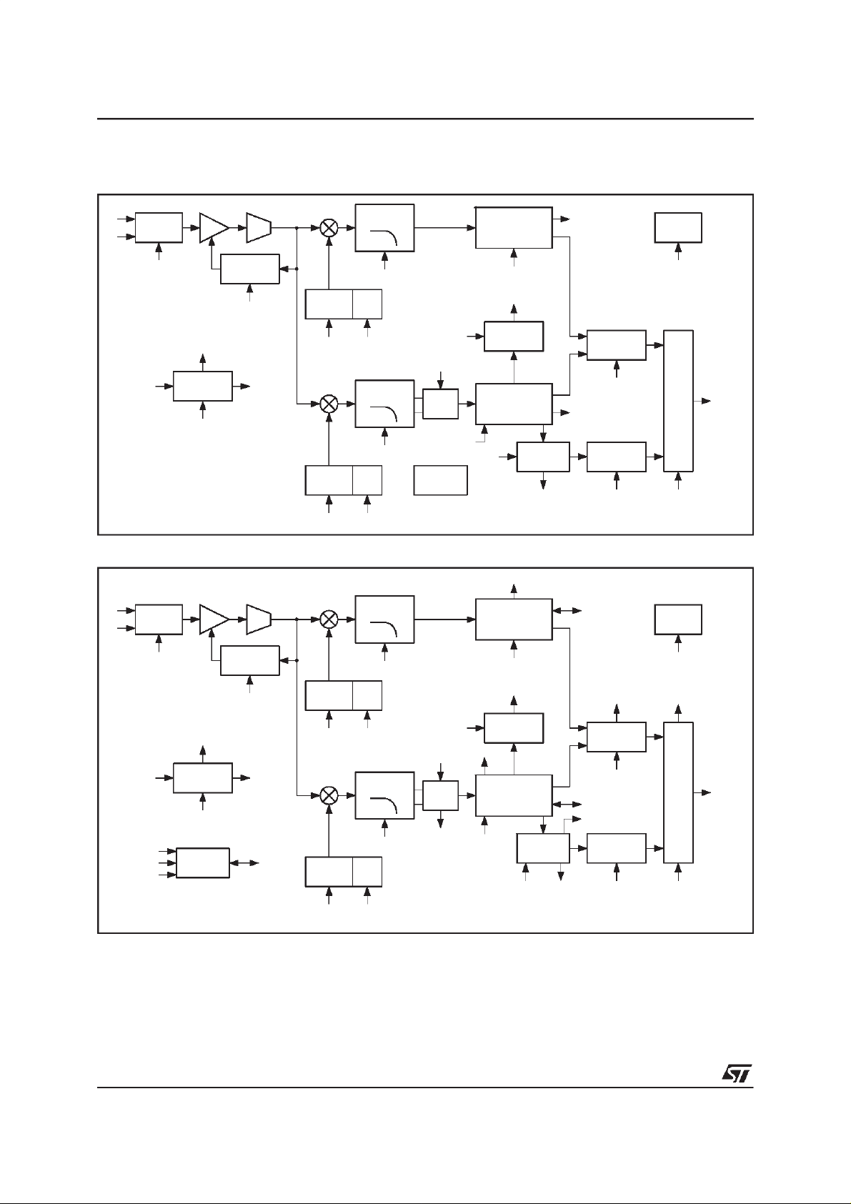
BLOCKDIAGRAM
SIF1
SIF2
ANALOG
SWITCH
AGC
Sub
IN
DEMODULATOR CORE *
XTAL
DV
AV
DD5
CC
CRYSTAL
OSCILLATOR
POWER SUPPLY
REGULATORS
Digital
Analog
STV8203
* See Demodulator Core Block Diagram
DEMODULATORCORE BLOCKDIAGRAM
Sub
ADC
IN
BAND
PASS
FM
DISCRIMINATOR
FM / NICAM
2
AUDIO MATRIX
22
PRE-SCALING
MONO IN
SCART1 IN L
SCART1 IN R
NOISE*
ESTIMATION
SCART2 IN L
L1, R1
(L1 + R1)/2
SCART2 IN R
2
C BUS
I
INTERFACE
2
2V
2
2V
1V
SIGNAL
SHAPING
RMS
RMS
RMS
PRE-SCALING
SDA
SCL
SCART1 OUT L
SCART1 OUT R
SCART2 OUT L
SCART2 OUT R
MONO OUT
ONE BIT
SIGMA
DELTA
DAC
8203-03.EPS
Channel 1
* Data also available throught I
4/31
LEVEL *
ESTIMATOR
BAND
PASS
DISCRIMINATOR
2
C Bus
FM
NICAM QPSK
AND
DECODER
SOUND STANDARD MANAGEMENT
IDENTIFICATION,
CHANNEL CONTROL, MUTE, ...
PILOT *
RECOGNITION
NOISE*
ESTIMATION
QPSK LOCK *
DETECTION
BIT ERROR
RATE *
DIGITAL CHANNEL MATRIX AND AUTOSWITCH
SIGNAL
SHAPING
2
I
C Bus
ONE BIT
SIGMA
DELTA
PRE-SCALING
DAC
Channel 2
8203-04.EPS
Page 5
FUNCTIONAL DESCRIPTION
Ascanbe seen fromthe blockdiagram,theinputto
the demodulatorsection is selectablefrom one of
twoI.F.sourcesviathe I
2
Cbus.Theselectedsignal
is then passed through an AGC block, having a
range of 28dB, before being digitised in the
ADCunit.Asinglequartzcrystal(suggestedvalue:
between24.712MHzand 27MHz)is usedforthe all
thedigitalprocessing,includingdemodulation,identification, control, filtering. This has the advantage
ofa singleclocksignalsourceforthewholeICwhich
eliminates problems of multiple clock. The single
clock canbe chosento minimize interferencein the
TVIF andRF stagesof the tuner system.
Thedemodulatorsystemcan identifyand demodulateallthestandarddescribedintheTable1. Theresult of the recognition is flagged up to the host
system via the I
2
C buscommunicationsystem.
In the case of NICAM transmissions, in the event
of a failure of the received signal or a degradation
ofthe bit error rate (BER)belowa prescribedlevel,
thesystem will automaticallydefault to the reserve
soundtransmission on mono FM or AM.
For FM demodulation, the discriminator can normallyhandlesignalshaving250kHzdeviation.This
covers all European standards, and ensure an
optimizedcompromise for thesignal to noiseratio
inonehand,andovermodulationintheotherhand.
However, it is possible to extand the deviation
rangeupto 500kHz(I
2
Cprogrammable)in orderto
coverrequests of some broadcasters.
Fully automatic standard recognition and setting
canbe achieveusing simple routines.
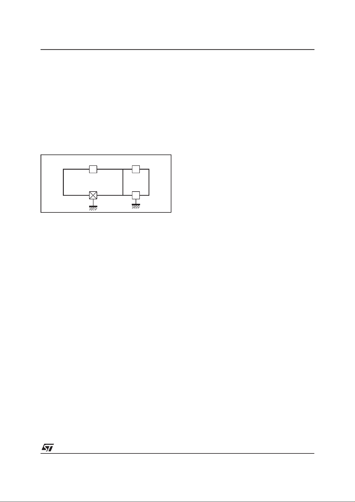
Figure1 : AudioMatrix
2
DAC
LI2(SCART2)
MIN
LI1(SCART1)
MUTE
2
S1
GAIN
± 6dB
2
S2
Appropriate de-emphasis networks in the digital
domain are applied to the resulting demodulated
signals (50µs, J17), followed by dematrixing if required. The digital datastream is then passed
through2 x 16bits DACs before the audio matrix.
All thisfirst section is workingat 3.3Vthanks to an
integratedvoltageregulator.In stand-bymode,the
voltage regulator pulls the voltage down to zero,
ensuringno power dissipationin thispart.
An audio matrix allows the selection of inputs appliedontheoutputsSCART1,SCART2andMONO
accordingto the diagram shown in Figure1.
The ”MOUT”outputs eitherthe signal L1, or R1 or
(L1+R1)/2.Thisallowstorecordtheselectedchannel in monomode, for exampleon thelinear channel of a VCR simultanously with the stereo mode.
Maximumoutput swingis 1V
RMS
.
The audio matrixsection has its own power supply
regulator,allowing to keep this part working even
when the rest is instand-bymode. Thisachievesa
”THRU” mode from input ”SCART1” to output
”SCART2”andinput”SCART2”tooutput”SCART1”.
The maximumoutput swing of both SCART1 and
SCART2is 2V
RMS
.
Remark : Circuit operationis possible with only a
single5V supply.In thiscase, the AV
CC
is connectedto 5V.Maximumoutput swingis then
limitedto 1V
anda 6dBattenuationis automat-
RMS
ically added to the DAC output. In that case, the
resistorshown as R2 =39Ωin theApplicationDiagram (between Pin 8 and Pin 21) must be replace
by a short circuit to avoid clipping.
MUTE
MUTE
L1/R1
L1,R1,
(L1 + R1)/2
SELECTOR
L2/R2
2
2
AO1(SCART1)
MOUT
AO2(SCART2)
STV8203
supplypin
8203-05.EPS
5/31
Page 6
STV8203
FUNCTIONAL DESCRIPTION(continued)
Table1 :DemodulatedTV SoundNorms
Type
System Sound Type
FM mono 5.5
B/G
FM/NICAM 5.5 5.850 27 50 80 J17 40
FM 2 carriers A2 5.5 5.742 27 50 80 50µs 54.6875
B/H FM/NICAM 5.5 5.850 27 50 80 J17 40
FM mono 6.5
D/K
FM/NICAM 6.5 5.850 27 50 80 J17 40
D/K1 FM 2 carriers A2* 6.5 6.258 50µs 54.6875
D/K2 FM 2 carriers 6.5 6.742 50µs 54.6875
FM/NICAM 6.0 6.552 27 50 80 J17 100
I
FM mono 6.0 50µs
L NICAM 6.5 (1) 5.850 J17 40
M/N FM mono 4.5 (2) 15 25 50 (2)
Notes : 1. STV8203 performs only limitedAM demodulation. Report to Application Note.
2. 50µs only, instead of 75µs.
Name
Carrier 1
(kHz)
Carrier 2
(kHz)
FM Deviation (kHz)
Nom. Max. Over
Deemphasis Roll-off
Frequency
Pilot
(kHz)
6/31
Page 7
USINGSTV8203
1 - Hardware
1.a - PowerSupplies (see Figure 2)
TheIC is usingtwo mainpower supplies:
-DV
supplies all the digital part V
DD5
Nom.
=5V.
This power supply can be switched-off in standby mode.
-AV
suppliestheaudio matrixpart : ifV
CC
Nom.
then the output voltage swing on outputpins can
reach2V
RMS
,ifV
swing on outputpins can reach 1V
=5Vthentheoutputvoltage
Nom.
RMS
.
Figure2
DV
DD5
41
DEMODULATION
ANDCONTROLPART
Pins5-32-42
GND
AV
CC
21
AUDIO
MATRIX
11
GND
=8V
STV8203
between stereo or mono signals in the playback
modein case of marginalnoise conditions.
1.d - Stand-by
Stand-bywith THRU mode : theanalogpartof the
device has its own power supply (AV
thispart to keepworkingevenwhenthedigitalpart,
powered by the 5V power supply (DV
stand-by.
In this case, the audio matrix is put in a special
setting:
- LIL1 to AOL2,
- LIR1 to AOR2,
- LIL2 to AOL1,
- LIR2 to AOR1,
- input gain = 0dB.
This allows to achieve a ”THRU” mode from
SCART1 input to SCART2 output and SCART2
input to SCART1 output, providing a copy facility
fromSCARTINto SCARTOUT.
8203-06.EPS
) allowing
CC
DD5
), is in
1.b- Sound Subcarrier Filters
Sound demodulation and decoding are very easy
withthisdeviceprovidingallthenecessaryfunctions
for that purpose, including the channel filters.
TheseFIRbase-bandfiltersgivethe bestselectivity
ofthedesiredchannelandprovidesinNICAMmode
thecorrectcosine roll-off response.
This implies that no external filters are required
(exceptmay be a simplehigh-passfilter,ifthe saw
filters and sound IF demodulators used in the applicationcreate picture interferences).
Thefilterscan beautomaticallyset forB/G/H/I/L/L’
standards.They can alsobe easily tuned through
2
C for M, D, K, K1.
I
1.c- AudioMatrix
The mono output (MOUT) can output L1, R1 or
(L1+R1)/2 signal.A typicalapplicationis the possibilityto recorda selectedchannelin monomodeon
thelineartrackofa VCRseparatelyfromtherecordingofthestereosignal,providingthefacilitytoselect
2 - Software
Twomodes of operationare available:
2.a - OptimizedProgram Mode
Fourstandardshavedefaultsettingstoredin order
to allow a very easy programmation. Only some
registersmay have to be programmed(these registersare shownin bold in theFigure3)but inmost
cases, the reset values will be sufficient. In Figure3, CTLand STATrepresentregisterswhich are
controlledby the ”standardprocessor”.These registers are located between address 23Hex and
3CHex in thecomplete list of registers.
2.b - AdvancedOperationMode
In that mode, all the read/write registers (as mentionned in the complete list) can be programmed
manuallyand changedfromtheir reset values.
The additionnal registers accessible in this mode
are shown in bold in Figure 4. This mode can be
selectedby putting the bits [3:0] of AO-CONTROL
registerto 0.
7/31
Page 8
STV8203
USINGSTV8203 (continued)
Figure3 : Optimized Program Mode
IF1
IF2
INPUT
SWITCH
PRE-LINE-IN
STAT
AGC
AO-STAT0
AO-STAT1
AO-STAT2
AUTO
STANDARD
AO-CONTROL
AO-TIMEOUT
ADC
LEVEL
DETECTOR
AGCC
AGCS
CTL
CH1
DCO
COARSE
CTL
CH2
DCO
COARSE
Figure4 : AdvancedOperation Mode
IF1
IF2
INPUT
SWITCH
AGC
ADC
CH1
CHANNEL
FILTERFIR1
CTL
DCO
FINE
CTL
CHANNEL
FILTERFIR2
CTL
DCO
FINE
CTLCTL
CHANNEL
FILTERFIR1
ZWEITON
CTL
AGC
INPUT
CETH2
SQTH2
CLOCK
CONTROL
PLL
DEMODULATOR
FM
CETH1 - SQTH1
STAT
ZWEITON
DETECTOR
PLL
DEMODULATOR
FM/QPSK
NICON
STAT(2)
PLL
DEMODULATOR
FM
NICAM
DECODER
STAT
STAT
STAT
CRF1
FM
PRESCALE
PRE-FM
NICAM
PRESCALE
PRE-NICAM
AUDIO
MATRIX
PRE-LINE-IN
AUD-MX-CNT
DE-EMPHASIS
SWITCHDE-MATRIX
CTL
AUDIO
MATRIX
To
DAC’s
8203-07.EPS
PRE-LINE-IN
STAT
(1),(2) or (3)
FFFIXL
FFFIXH
FCFIX
(1)
Bitsin AO-STAT0
(2) Bitsin AO-STAT1
(3) Bitsin AO-STAT2
AO-STAT0
AO-STAT1
AO-STAT2
AUTO
STANDARD
AO-CONTROL
AO-TIMEOUT
CLOCK
CONTROL
LEVEL
DETECTOR
AGCC
AGCS
CTL
SRF
DCO
CH2
DCO
DCO
FINE
FILTERFIR2
DCO
FINE
COARSE
COFQ1 FIFQ1
COARSE
COFQ2 FIFQ2
FIR1CO-7
CHANNEL
FIR2CO-7
ZWEITON
IAGCR
IAGCC
AGC
INPUT
IAGCS
CETH1- SQTH1
ACOEFF1 - BCOEFF1
STAT(2)
ZWEITON
DETECTOR
STAT(2)
PLL
DEMODULATOR
FM/QPSK
CETH2
SQTH2
ACOEFF2
BCOEFF2
SCOEFF
NICAM
DECODER
NICON ERR-
COUNT
PRE-LINE-IN
AUD-MX-CNT
FMDC1/2 STAT(1)
FM
PRESCALE
PRE-FM
CRF2
STAT(3)
NICAM
PRESCALE
PRE-NICAM
DE-EMPHASIS
SWITCHDE-MATRIX
STD-CT-IIS
To
DAC’s
8203-08.EPS
8/31
Page 9
USINGSTV8203 (continued)
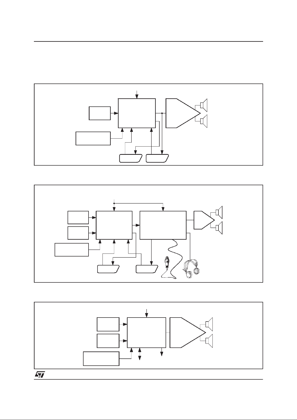
3 - Example of Applications
3.a - VeryLow Cost TVApplication
Figure5
2
C Control
I
STV8203
TUNER1
QSS I.F.
AM
DEMODULATOR
3.b- High-End TV Application
Figure6
TUNER 1
QSS I.F.
TUNER 2
QSS I.F.
AM
DEMODULATOR
MULTISTANDARD
MULTISTANDARD
2
C Control
I
SOUND
PROCESSOR
STV8203
SOUND
PROCESSOR
STV8203
SCART1 SCART2
AUDIO
PROCESSOR
SURROUND/KARAOKE
SRS
TDA7466
AUDIO
AMPLIFIER
TDA7495
2x7W
8203-09.EPS
R
2 x 25W
L
3.c - TVApplication in PC
Figure7
DEMODULATOR
SCART1 SCART2
I2C Control
TUNER1
QSSI.F.
TUNER2
QSSI.F.
MULTISTANDARD
SOUND
PROCESSOR
STV8203
AM
I2S Bus
Analog
AudioOut
8203-10.EPS
AUDIO
AMPLIFIER
TDA7495
8203-11.EPS
9/31
Page 10
STV8203
ABSOLUTE MAXIMUMRATINGS
Symbol Parameter Value Unit
AV
DD5
DV
DD5
AV
CC
P
tot
T
oper
T
stg
THERMAL DATA
Symbol Parameter Value Unit
R
th (j-p)
RECOMMENDEDOPERATING CONDITIONS
Symbol Parameter Min. Typ. Max. Unit
AV
DD5
DV
DD5
AV
CC
Analog Supply Voltage 7 V
Digital Supply Voltage 7 V
Scart Interface Supply Voltage 9.5 V
Power Total Dissipation 0.8 W
Operating Temperature 0, +70
Storage Temperature -20, +150
Junction to PinsThermal Resistance Max.
Analog V
Digital V
DD
DD
Audio Interface Supply for 2V
for 1V
RMS
RMS
SDIP42
TQFP44
outputs
outputs
4.75 5.0 5.25 V
4.75 5.0 5.25 V
7.6
4.75
55
68
8.0
5.0
8.4
5.25
o
C
o
C
°C/W
°C/W
V
V
8203-02.TBL
8203-03.TBL
8203-04.TBL
ELECTRICAL CHARACTERISTICS (T
=25oC, unless otherwise specified)
amb
Symbol Parameter Test Conditions Min. Typ. Max. Unit
GENERAL
I
I
Input Currenton AV
AIN
DIN
CC
AVCC=5V
=8V
AV
CC
DV
= 5V 120 mA
DD5
58
75
IF INPUTS
R
C
Input Resistance 6 kΩ
IN
Input Capacitance 10 pF
IN
SWISO Switch Isolation f = 10MHz 40 dB
SIF FR Input Frequency Range For FM demodulation 4 8 MHz
V
IN (Min.)
V
IN (Max.)
Minimum InputLevel
Maximum Input Level
25
630
mV
mV
AGC AGC Range 28 dB
mA
mA
RMS
RMS
8203-05.TBL
10/31
Page 11

STV8203
ELECTRICAL CHARACTERISTICS (T
=25oC, unless otherwise specified) (continued)
amb
Symbol Parameter Test Conditions Min. Typ. Max. Unit
FM DEMODULATION PATH (see Figure8)
f
RESP
SNR FM Signal to Noise 100mV
THD FM Total Harmonic Distortion Output signal 1V
SEP FM German Stereo Channel
Frequency Response 20Hz - 15kHz -1.0 +1.0 dB
, unweighted20Hz-15kHz,
RMS
Output 2V
50kHz FM deviation
RMS
@ 1kHz
RMS
@ 1kHz,
65 dB
0.2 %
40 dB
Separation
AMR AM Rejection SIF = 100mV
30% modulation @ 1kHz
V
FMOUT
Maximum OutputSwing 2 V
RMS
60 dB
NICAM DEMODULATION PATH (see Figure8)
SNR NIC Signal to Noise 100mV
Output 2V
, unweighted20Hz-15kHz,
RMS
@ 1kHz
RMS
THD NIC Total Harmonic Distortion Output signal 1V
V
NICOUT
Maximum OutputSwing 2 V
@ 1kHz 0.07 %
RMS
72 dB
SEP NIC Channel Separation 60 dB
AUDIO MATRIX (see Figure 9)
RIN Input Resistance 30 kΩ
V
Input ClippingLevel AVCC=8V
CL
AV
CC
=5V
GMAT Prescaling = 0
=1V
V
IN
R
Output Resistance All audio output except Mono output
OUT
Mono output
, 15Hz to 15kHz
RMS
SNR Signal to Noise Ratio Preline in = 0,
=2V
V
OUT
RMS
XLR Audio L to R Channel Crosstalk
2V
@ 1kHz
X12 Audio Crosstalk from Channel 1
RMS
2
1
-0.5 0 0.5 dB
200
400
90 dB
,unweighted 20Hz-15kHz
60 dB
80 dB
V
V
to Channel 2
RMS
RMS
RMS
RMS
Ω
Ω
8203-06.TBL
Figure8 : SynopticA
SIF1
Figure8 : SynopticA
AIL1 or 2
or
AIR1 or 2
DIGITAL
DEMODULATATION
STV8203
STV8203
DAC
Analog
Switch
Analog
Switch
AOL1
or AOR1
8203-12.EPS
AOL1or 2
or
AOR1 or 2
8203-13.EPS
11/31
Page 12

STV8203
PROGRAMMING THE DEVICE
2
1-I
C Addressand Protocol
Write
S 80 A SUB-ADDRESS A DATA A DATA A P
Read
S 80 A SUB-ADDRESS A P S 81 A DATA A DATA N
S = Start, A= Acknowledge, P =Stop, N = No acknowledge.
Sub-addressis the registeraddresspointer ; thisvalue auto-incrementsfor bothwrite and read.
2 - List of Registers
Registersnot controlled by AUTOSTANDARD, except bits marked ”*” which are controlled
Name
SWD (Switch, Dematrix & De-emphasis)
PRE-FM 2 0001 1101 0 0 0 Fm Prescale [4:0]
PRE-NICAM 3 0001 1101 0 0 0 Nicam Prescale [4:0]
STD-CT-IIS 4 0001 1000 0 0 gain demoff mute * SWD [2:0] *
FMDC1 5 read only FM DC level 1
FMDC2 6 read only FM DC level 2
AUDIO MATRIX
PRE-LINE-IN 7 0000 1000 IF Switch AGC
AUD-MX-CNT 8 0010 0010 mout1 S1 o/pselect mout0 S2 o/p select
NICAM
NICON 9 0000 0000 dif-pol 0 TSCTRL [1:0] ECT MAE 0 0
ERR-COUNT A read only error [7:0]
AUTOSTANDARD
AO-STAT0 B read only std-det sid1 sid0 aomute am-mono SWD [2:0] (monitor)
AO-STAT1 C read only fm2-car fm2-sq fm1-car fm1-sq qpsk-lk zw-det zw-st zw-dm
AO-STAT2 D read only nic-det f-mute LOA Nicam CBI [4:1] n-mute
AO-CONTROL E 0001 1111 muteov mono ov unmute C4 ov standard check [3:0]
AO-TIMEOUT F 1010 0101 Time 2 setting (1280ms) Time 1 setting (160ms)
ZWEITON
ZWEITON 10 1000 1000 Thresh-Sig [3:0] Thresh-ST [3:0]
DEMODULATOR
AGCC 11 0001 0001 agc-cmd* 0 0 agc-ref [2:0] agc-cst[1:0]
AGCS 12 0100 00xx 0 agc-err [4:0] sig-ovr sig-und
IAGCR 14 1000 1000 Iagc-ref [7:0]
IAGCC 15 0000 0011 iagc-off* 0 0 0 0 Iagc-cst[2:0]
IAGCS 16 read only Iagc-Ctrl [7:0]
FFFIXL 17 0000 0000 Clock Generator Fine Frequency (8 lsb’s)
FFFIXH 18 01101110 0 demod mode M2:M0* clock gen fine freq (4 msb’s)
FCFIX 19 0001 0001 0 0 Clock Generator Coarse Frequency
CRF2 20 0000 0000 Channel 2 CarrierRecovery Frequency
CETH2 21 0011 0101 Channel 2 carrier-th[7:0]
SQTH2 22 0011 1100 Channel 2 squelch-th[7:0]
Range of Registers Controlled by AUTOSTANDARD Function (address 23 Hex to 3CHex)
CRF1 3D 00000000 Channel 1 CarrierRecovery Frequency
CETH1 3E 0011 0101 Channel 1 carrier-th[7:0]
SQTH1 3F 0011 1100 Channel 1 squelch-th [7:0]
Addr.
(Hex)
Reset
(Bin)
bit 7 bit 6 bit 5 bit 4 bit 3 bit 2 bit 1 bit 0
Switch off
Register Function /Description
0 0 Line Inputs Gain[3:0]
12/31
Page 13

PROGRAMMING THE DEVICE (continued)
Registerscontrollableby AUTOSTANDARD
Name
DEMODULATOR CHANNEL 2
FIR2CO 23 0000 0000 FIR2 coefficient 0
FIR2C1 24 0000 0000 FIR2 coefficient 1
FIR2C2 25 0000 0000 FIR2 coefficient 2
FIR2C3 26 0000 0000 FIR2 coefficient 3
FIR2C4 27 1111 1111 FIR2 coefficient 4
FIR2C5 28 0000 0100 FIR2 coefficient 5
FIR2C6 29 0001 0100 FIR2 coefficient 6
FIR2C7 2A 0010 0101 FIR2 coefficient 7
COFQ2 2B 0000 1100 0 0 Channel 2 DCO Coarse Frequency
FIFQ2 2C 1100 0100 Channel 2 DCO Fine Frequency (8lsb’s)
ACOEFF2 2D 1001 0000 dmd sw2 0 Coarse A2 Sign A2 Fine A2
BCOEFF2 2E 1010 1100 sat sw2 0 dco2 gain B2
SCOEFF 2F 0001 1100 dmx-of 0 plf_A plf_B
SRF 30 0000 0000 Symbol Recovery Frequency
DEMODULATOR CHANNEL 1
FIR1CO 31 0000 0000 FIR1 coefficient 0
FIR1C1 32 1111 1110 FIR1 coefficient 1
FIR1C2 33 1111 1100 FIR1 coefficient 2
FIR1C3 34 1111 1101 FIR1 coefficient 3
FIR1C4 35 0000 0010 FIR1 coefficient 4
FIR1C5 36 0000 1101 FIR1 coefficient 5
FIR1C6 37 0001 1000 FIR1 coefficient 6
FIR1C7 38 0001 1111 FIR1 coefficient 7
COFQ1 39 0000 1011 0 0 Channel 1 DCOCoarse Frequency
FIFQ1 3A 1100 0111 Channel 1 DCO Fine Frequency (8lsb’s)
ACOEFF1 3B 0010 0011 dmd sw1 0 Coarse A1 Sign A1 Fine A1
BCOEFF1 3C 0001 0010 sat-sw1 0 dco1 gain B1
Addr.
(Hex)
Reset
(Bin)
bit 7 bit 6 bit 5 bit 4 bit 3 bit 2 bit 1 bit 0
Register Function/Description
STV8203
Note : This register must be kept to ”0”.
RESERVED 1 00000000 0 0000000
13/31
Page 14

STV8203
PROGRAMMING THE DEVICE (continued)
3 - RegisterDescription
3.1 - RegistersNot Controlled By Autostandard(except some mentionedbits)
PRE-FM(Prescale FM Level)
Address : 02
Type : R/W
Reset : 0001 1101
bit 7 bit 6 bit 5 bit 4 bit 3 bit 2 bit 1 bit 0
0 0 0 FM PRESCALE
FMPRESCALE : 00000
01100
10100
0dB
+12dB
-12dB
(stepsize = 1dB,range = ±12dB in 2’s complement)
Sets the reference level for an FM signal. Note, this is also dependant on the PLL programming. For
example,with default settings forthe PLL, an FM deviationof 27kHz will result in a signal17dB below full
scalebeforede-emphasis. At1kHz, the internalde-emphasisgain is14dB giving a levelof -3dB.Fullscale
output from the DAC is 2V
correspondingto 0dB.and so for 1V
RMS
, PRE-FMshould be set to -3dB.
RMS
PRE-NICAM (PrescaleNICAM Level)
Address : 03
Type : R/W
Reset : 0001 1101
bit 7 bit 6 bit 5 bit 4 bit 3 bit 2 bit 1 bit 0
0 0 0 NICAM PRESCALE
NICAMPRESCALE : 00000
01100
10100
0dB
+12dB
-12dB
(step size = 1dB, range= ±12dB in 2’s complement)
Sets the reference level for a NICAM signal. For example, a full scale NICAM signal at 1kHz would be
received at -12dB before de-emphasis. Internal de-emphasis gainat this frequencyis 9dB so for 1V
RMS
pre-nicamshould be set to -3dB.
,
14/31
Page 15

STV8203
PROGRAMMING THE DEVICE (continued)
STD-CT-IIS
Address : 04
Type : R/W
Reset : 0001 1000
bit 7 bit 6 bit 5 bit 4 bit 3 bit 2 bit 1 bit 0
GAIN : whichshould normallybe set to itsdefault value, can be used to changethe dematrixgain
DEMOFF : bypassesthe FM or Nicam de-emphasis: 1 =de-emphasisoff
MUTE : mutes the DAC(FM or Nicam) : 1 = DAC muted
SWD : Bits allow control of the modeof the switch/dematrixfunction as shownbelow.
(SWDControl)
0 0 GAIN DEMOFF MUTE SWD
for CH1 = L+R.
dematrixgain : 0 : channel1 = L/2+R/2,1 : channel1 = L+R
(onlyeffective if the AUTOSTANDARDfunction is off)
(onlyeffective if the AUTOSTANDARDfunction is off)
[2:0] De-emphasis Description NICON[1:0] Left Right
000
001 Zweiton mono X D1 D1
010 Zweiton dual mono
011 Zweiton stereo X DSL DSR
100 not used
101
110 Nicam dual mono
111 Nicam stereo X NSL NSR
50µs
J17
FM CH1 mono X D1 D1
00 D1 D2
01 D2 D2
10 D1 D1
11 D2 D1
Nicam mono X N1 N1
00 N1 N2
01 N2 N2
10 N1 N1
11 N2 N1
D1 = FM audio from CH1,D2 = FMaudio from CH2, DS = dematrixedZweitonstereo.
N1 = NicamM1, N2 = Nicam M2, NS = Nicamstereo.
These bits are controlledby AUTOSTANDARDwhen this function is activated.
FMDC1, FMDC2
(FM DC Level)
Address : 05-06
Type : R
bit 7 bit 6 bit 5 bit 4 bit 3 bit 2 bit 1 bit 0
FM DC LEVEL 1 OR FM DC LEVEL 2
FMFrequencyoffset (dependenton thePLL coefficients).
This value (2’s complement) is proportional to the DC offset, measured below 20Hz, of an FM signal. It
could be used to implement an AFC for FM signals.
15/31
Page 16

STV8203
PROGRAMMING THE DEVICE (continued)
PRE-LINE-IN
Address : 07
Type : R/W
Reset : 0000 1000
bit 7 bit 6 bit 5 bit 4 bit 3 bit 2 bit 1 bit 0
IF SWITCH AGC SWITCH OFF 0 0 LINEINPUTS GAIN
IF SWITCH : IF InputSwitch
AGC SWITCHOFF : can be used to switch-offthe AGC amplifier..
LINEINPUTS GAIN : allow the levels of the analog line inputs (SCART1, SCART2and MONO) to be
AUD-MX-CNT (AudioMatrix Control)
Address : 08
Type : R/W
Reset : 0010 0010
(IF Input Selectionand Audio Matrix Gain Control)
controlsthe IF inputselection (0 = IF1).
adjusted simultaneously.
1000
0010
1110
0dB
-6dB
+6dB
(defaultsetting)
(step size = 1dB, range=±6dB)
bit 7 bit 6 bit 5 bit 4 bit 3 bit 2 bit 1 bit 0
MOUT1 S1 O/P SELECT MOUT0 S2 O/P SELECT
These8 bits are usedto controlthe audiomatrixconfiguration(see Figure1).
Data bits Actual Function Selected
76543210Reset : AO1 and AO2 = DAC and MOUT = (L1+R1)/2
XXXXX000AO2=Muted
XXXXX001AO2=Muted
XXXXX010AO2=AO1(reset state)
XXXXX011AO2=LI1(Scart 1 input)
XXXXX100AO2=Muted
XXXXX101AO2=Muted
XXXXX110AO2=Muted
XXXXX111AO2=Muted
X 0 0 0 X X X X AO1 = Muted
X 0 0 1 X X X X AO1 = MIN
X 0 1 0 X X X X AO1 = DAC (reset state)
X 0 1 1 X X X X AO1 = Muted
X 1 0 0 X X X X AO1 = LI2 (Scart 2 input)
X 1 0 1 X X X X AO1 = Muted
X 1 1 0 X X X X AO1 = Muted
X 1 1 1 X X X X AO1 = Muted
0 X X X 0 X X X MOUT = (L1+R1)/2 (reset state)
0XXX1XXXMOUT=R1
1XXX0XXXMOUT=L1
1 X X X 1 X X X Notused
16/31
Page 17

STV8203
PROGRAMMING THE DEVICE (continued)
NICON
Address : 09
Type : R/W
Reset : 0000 0000
DIF-POL : controls the polarity of the Q channelin the DQPSKdecoder.Its default value is correctfor
TSCTRL : These two bits are programmed to chose the decision mode for the zweiton detector as
ECT : bit error rate counting time : 0 = 128ms,1 = 64ms
MAE : max allowed errors : 0 = 511,1 = 255
(NICAMControl)
bit 7 bit 6 bit 5 bit 4 bit 3 bit 2 bit 1 bit 0
DIF-POL 0 TSCTRL ECT MAE 0 0
NicamB/G/L and so doesnot need to be changed.
following:
00
:
2 decisionswith 1024 samples accumulation
01
:
3 decisionswith 1024 samples accumulation
10
:
2 decisionswith 2048 samples accumulation
11
:
3 decisionswith 2048 samples accumulation
Bits2 and3 adjustthebit error rate(approximate)atwhichtheNicam decodermutes;a fixed
hysteresis is provided so that the decoder will unmute only when the BER hasdropped to
one quarter of that for muting :
ECT MAE BER Muting Threshold
0 0 1 in 112
0 1 1 in 224
10 1in56
1 1 1 in 112
ERR-COUNT
(NicamError Counter)
Address : 0A
Type : R
bit 7 bit 6 bit 5 bit 4 bit 3 bit 2 bit 1 bit 0
ERROR
ErrorSignals Count (averagedover timeECTabove)
Thevalue in this register,updated every 64msor 128ms,gives anindication of theNicam bit error rate. It
canthereforebe usedto mutethe decoderat an errorrate below 1 in 56 (=FF if ECT=64ms).
17/31
Page 18

STV8203
PROGRAMMING THE DEVICE (continued)
AO-STAT0
Address : 0B
Type : R
bit 7 bit 6 bit 5 bit 4 bit 3 bit 2 bit 1 bit 0
STD-DET SID1 SID0 AOMUTE AM-MONO SWD (MONITOR)
STD-DET : StandardDetection :
SID [1:0] : StandardIdentification of the demodulatorinput
AOMUTE : Audio Output Mute
AM-MONO : AM selected
SWD : Switch DematrixMode
(AUTOSTANDARDStatus 0)
0 = no standard detected
1 = indicatesthat an expectedstandard has beenidentified.
indicatethe standardwhich has been identified :
SID[1:0] Standard
00 I FM/NICAM
01 B/G FM - Zweiton
10 B/G FM/NICAM
11 L/L’ AM/NICAM
indicatesthat the audiooutputs are muted(=1); onlywhen the demodulatoris selected as
audio source. This wouldbe the case during standardsearch or no signal found.
indicates if the AMinput (MIN) has been selected(=1); normallyused for system L.
indicatethe setting of the SWD block:
SWD[2:0] Mode description De-emphasis
000 FM CH1 mono
001 Zweiton mono (CH1)
010 Zweiton dual mono
011 Zweiton stereo
100 Unused Unused
101 NICAM mono
110 NICAM dual mono
111 NICAM stereo
50µs
J-17
AO-STAT1 (AUTOSTANDARD Status 1 ; demodulatorsignal detectors)
Address : 0C
Type : R
bit 7 bit 6 bit 5 bit 4 bit 3 bit 2 bit 1 bit 0
FM2-CAR FM2-SQ FM1-CAR FM1-SQ QPSK-LK ZW-DET ZW-ST ZW-DM
FM2-CAR : FM2 CarrierDetector Lock
FM2-SQ : FM2 Squelch Detector Lock
FM1-CAR : FM1 CarrierDetector Lock
FM1-SQ : FM1 Squelch Detector Lock
QPSK-LK : QPSKLock
ZW-DET : ZweitonPilot Lock
ZW-ST : Zweiton Stereo Lock
ZW-DM : Zweiton Dual Mono Lock
This registerallows direct access to the demodulatorsignal detectors; 1 = detected.
18/31
Page 19

STV8203
PROGRAMMING THE DEVICE (continued)
AO-STAT2
Address : 0D
Type : R
bit 7 bit 6 bit 5 bit 4 bit 3 bit 2 bit 1 bit 0
NIC-DET F-MUTE LOA NICAM CBI N-MUTE
NIC-DET : NICAM detected
F-MUTE : Frame Mute
LOA : Loss of frame Alignmentword
NICAMCBI : indicates the receivedNICAM control bitswith the followinginterpretation:
(AUTOSTANDARDStatus 2 ; NICAM)
indicates a validNICAM signal found(1 = detected).
indicatesthe NICAMdecoder is mutedbecausethe superframealignment has been lost.
indicateslossof alignmenttothe framealignment wordin the NICAMdecoder;thebiterror
rate istoo highor no signal is present.
CBI[4:1] Nicam Signal Description
X000 Stereo
X001 ch1 = mono, ch2 = data
X010 Dual Mono
X011 704Kbit/sdata
X1XX FM selected during additional coding options
0XXX Nicam different to FM mono
1XXX Nicam mono(M1) or stereo = FM mono
N-MUTE : NICAM Mute
indicates that the NICAMdecoder is muted(it may be unmutedby AO-CONTROL bit 5).
19/31
Page 20

STV8203
PROGRAMMING THE DEVICE (continued)
AO-CONTROL(AUTOSTANDARDControl)
Address : 0E
Type : R/W
Reset : 0001 1111
bit 7 bit 6 bit 5 bit 4 bit 3 bit 2 bit 1 bit 0
MUTE OV MONO OV UNMUTE C4 OV STANDARD CHECK
AUTOSTANDARD controls the audio matrix when the user has selected the DAC as source(AUD-MXCNT bits[6:4] = 010).In thiscase it will mute theoutputs or select MIN. These functionscan be overriden
by bits 6 and 7 below.
MUTEOV : Mute override,1 = mute(overrideAUTOSTANDARD)
forcesthe audio signal to be muted.
MONOOV : FM/AM Mono override,1 = mono (overrideAUTOSTANDARD)forces
canbeusedto forceto analoguesound.This maybe usefulin thecaseof marginalNICAM
receptionto prevent automaticswitching.
AUD-MX-CNT bits[6:4] bit 7 bit 6 AO1 source
010 0 0 DAC
X 1 MIN (in case of L/L’ standard)
0 1 FM (in case of B/G or I standard)
1 1 Muted (in caseof B/G or I standard)
1 0 Muted
UNMUTE : Nicam Un-mute, 1 = unmute
allowsthe NICAMdecoder to be unmutedif the bit errorrateis higherthanthe preset limit;
this overrides the automatic switching to FMor AM which would normally occur.
C4 OV : CBI4 override, 1 =>CBI[4] forced to 1 internally
is usedto overridethe 4th NICAM controlbit (reservesound switch) if required.Thisbit is
transmitted by the broadcaster to indicatethat the analoguesound carrier is a backupof
the NICAM signal; this is usually the case. If the NICAM signal fails, the STV8203 will
automaticallyswitch to backup sound if the received bit was set to 1. If thisbit was set to
0 and bit 4 set to 0, the decoder will stay switched to analogue sound. If bit 4 is setto 1,
the received CBI4 is ignored. Note that if automatic standard is off, switching between
analogueand NICAMaudio must be done manually.
STANDARD
CHECK
: Controlthechoiceoftransmi ssionstandardstobesearchedforbytheautomaticstandar dfuncti on
(standardsearchactivewhenbit=1).Themorechoices,thelongerthesearchtime.Ifthesystem
in use canbe identifi ed by the charac teristi csof the vid eo signal, for exampleby the chroma
demodulator,thenonlya singlebitneedsto be set.In thiscase,theAUTOSTANDARDfuncti on
willprogramthedemodula torforthechosenstandard.Ifnobitsareset,theAUTOSTANDARD
functionis disabledandallregistersneedtobe setmanually.
bit 3- Runcheck for standard3 (L/L’- AM/NICAM)
bit 2- Run Check for Standard 2 (B/G - FM/NICAM)
bit 1- Run checkfor standard1 (B/G - Stereo)
bit 0- Run checkfor standard0 (I - FM/NICAM)
AO-TIMEOUT
(AUTOSTANDARDTimer Adjustment)
Address : 0F
Type : R/W
Reset : 1010 0101
bit 7 bit 6 bit 5 bit 4 bit 3 bit 2 bit 1 bit 0
TIME 2 SETTING TIME 1 SETTING
Time1 is used for NICAM and FM mono validation and time 2 for Zweiton. If the standard is not found
within this time limit, the next standard will be tried. Time 1 = decimal [bit 3:0] x 32ms. Time 2 = decimal[bit 7:4] x 128ms. Time 1 defaultvalue is 160ms.Time 2 defaultvalue is1280ms.
A time of 0ms should not be programmed.
20/31
Page 21

STV8203
PROGRAMMING THE DEVICE (continued)
ZWEITON
Address : 10
Type : R/W
Reset : 1000 1000
THRESH-SIG : PilotCarrier Level Threshold
THRESH-ST : Detected Tone Level Threshold
Poweron default values give a detectionthreshold correspondingto a modulatedpilot carrier S/N of 0dB
(700HzBW)and a S/Nof 40dB forthe recovered audio.
AGCC(AGC Controlfor ADC)
Address : 11
Type : R/W
Reset : 0001 0001
AGC-CMD 0 0 AGC-REF AGC-CST
(Pilot Carrier and Tone DetectorThresholds)
bit 7 bit 6 bit 5 bit 4 bit 3 bit 2 bit 1 bit 0
THRESH-SIG THRESH-ST
Set the sensitivityfor the pilot carrierdetector.
Set the detectionthresholdlevel forstereo and dual mono (bi-lingual) tones.
bit 7 bit 6 bit 5 bit 4 bit 3 bit 2 bit 1 bit 0
AGC-CMD : 1 = manual/forced mode, 0 = automaticmode
Normallyset to0 enablingautomaticmode. In the case of systemL/L’,due to the presence
of the AM sound carrier, the AGC should be switched off. In this case, a fixed gain value
should be set using the AGCS register(see below).
This bit is controlledby AUTOSTANDARDwhen thisfunctionis activated.
AGC-REF : Defines the clippinglevel.
Adjustthe allowableproportion of samplesat the input of the ADC which will be clipped;the
AGC tries to maximise the use of the full scale range of the ADC.The defaultsetting gives
a ratio of 1/256.
AGC-REF [4:2] Clipping Ratio
000 1/16 (single carrier)
001 1/32
010 1/64
011 1/128
100 1/256
101 1/512
110 1/1024
111 1/2048 (multiple carriers)
AGC-CST : AGC time constant betweeneach stepof 1.25dB.
For a 27MHzXTAL=> 00 = 1.21ms, 01 = 2.43ms,10 =4.85ms, 11 = 9.7ms.
The adjustmentis a compromisebetween settling time and noise immunity.
21/31
Page 22

STV8203
PROGRAMMING THE DEVICE (continued)
AGCS
Address : 12
Type : R/W
Reset : 0100 00XX
AGC-ERR : Gain Control Signal of amplifierbefore ADC. Thereare 32 steps of 1.25dB.
SIG-OVR
SIG-UND
IAGCR
Address : 14
Type : R/W
Reset : 1000 1000
(AGCControland Status for ADC)
bit 7 bit 6 bit 5 bit 4 bit 3 bit 2 bit 1 bit 0
0 AGC-ERR SIG-OVR SIG-UND
AGC-ERR [6:2] Gain (dB)
00000 0
00001 1.25
..... .....
11110 37.50
11111 38.75
When AGC_CMD= 0, AGC-ERRcan be read thusindicating the input level. It can alsobe
written to thus presettingthe AGC level which will then adjust itself to the finalvalue. When
AGC_CMD = 1, the AGC is off and thus writing to AGC-ERR directly controls the AGC
amplifier gain.Reading AGC_ERR just confirmsthe fixedvalue.
: 1 = agc overloaded - signaltoo BIG
1 = agc under loaded- signaltoo SMALL
When the AGC is in automaticmode (agc_cmd=0),bit 0 indicatesif the input signal is too
small and bit 1 if the AGC is too big. These bits couldbe used when setting the input level
to the STV8203.
(InternalAGC Referencefor QPSK)
bit 7 bit 6 bit 5 bit 4 bit 3 bit 2 bit 1 bit 0
IAGC-REF
Sets the mean value of the internal AGC, used for QPSKdemodulation. The default setting corresponds
to half full scaleamplitude at thePLL input.
IAGCC
(InternalAGC TimeConstant for QPSK)
Address : 15
Type : R/W
Reset : 0000 0011
bit 7 bit 6 bit 5 bit 4 bit 3 bit 2 bit 1 bit 0
IAGC-OFF 0000 IAGC-CST
IAGC-OFF : 1 = Internalagc = off
Onlyenabledwhen AUTOSTANDARDis off. Normally, theinternal AGCshouldbe OFFfor
FM and ON for QPSK.
This bit is controlledby AUTOSTANDARDwhen thisfunctionis activated.
IAGC-CST : InternalAGC ProgrammableStep Constant.
Set the internal AGC time constant; the compromise is between fast settling time (for the
quickestNicam identification)and noiseimmunity. Thecontrolrange is about 45dB divided
into 0.2dB steps. These bits controlthe timeper step (valuesgiven for QPSKmode) :
AGC-CST [2:0] Step time(µs) Time Response (ms)
000 703 105
001 352 53
..... ..... .....
111 5.5 0.82
22/31
Page 23

STV8203
PROGRAMMING THE DEVICE (continued)
IAGCS
Address : 16
Type : R
Indicatesthe valueof the internal AGC controlsignal.
Normally, the mean value should equal the value set in the IAGCR register when a signal is being
demodulated.
FFFIXL(ClockGenerator Fine frequency)
Address : 17
Type : R/W
Reset : 0000 0000
SeeFCFIX registerfor explanation.
FFFIXH
Address : 18
Type : R/W
Reset : 0110 1110
(InternalAGC ControlValue)
bit 7 bit 6 bit 5 bit 4 bit 3 bit 2 bit 1 bit 0
IAGC-CTRL
bit 7 bit 6 bit 5 bit 4 bit 3 bit 2 bit 1 bit 0
CLOCK GENERATOR FINE FREQUENCY (8 LSB’s)
(Clock Generatorand Fine Frequency Control)
bit 7 bit 6 bit 5 bit 4 bit 3 bit 2 bit 1 bit 0
0 DEMOD MODE M2:M0 CLOCK GEN FINE FREQ (4 MSB’s)
DEMODMODE M2:M0 : Controlsthe demodulatormode (only when registerEhex bits[3:0] = 0000):
MODE[6:4] CH1 FM CH2 FM/QPSK
X00 Normal FM Normal
X01 Wide FMWide
010 Normal QPSK System B/G/L
011 Wide QPSK System B/G/L
110 Normal QPSK System I
111 Wide QPSK System I
The FM discriminator modulationfull range can beset at :
- narrowmode : 250kHz(± 125kHz),
- widemode : 500kHz (± 250kHz).
CLOCKGEN FINEFREQ : Clock generator fine frequency (4 MSB’s)( seeFCFIX for explanation).
FCFIX (ClockGeneratorCoarse Frequency)
Address : 19
Type : R/W
Reset : 0001 0001
bit 7 bit 6 bit 5 bit 4 bit 3 bit 2 bit 1 bit 0
0 0 CLOCK GENERATOR COARSE FREQUENCY
Thebits [5:0]togetherwith FFFIXHbits [3:0] and FFFIXLbits [7:0]can be usedtoprogrammethe internal
clockgenerator for differentquartz crystal frequencies; thedefault value is for 27MHz.
P = 182 ⋅
Fref
Fqpsk
− 193 with Fref = crystalfrequency,Fqpsk =32 x 728kHz= 23.296MHz.
FCFIX= INT(P) (INT:integer part)
FFFIX= 256 x (16 x REM(P) - 1) (REM: fractionalremainder)
Notethat 0≤FFFIX<3840 so there is a small range of frequencieswhich cannot be used.
Example: Fref = 27MHz,FCFIX =17, FFFIX= 3584.
23/31
Page 24

STV8203
PROGRAMMING THE DEVICE (continued)
CRF2 - CRF1
Address : 20-3D
Type : R/W
Reset : 0000 0000
bit 7 bit 6 bit 5 bit 4 bit 3 bit 2 bit 1 bit 0
Thisregister providesaccess to the instantaneousfrequencyof the PLL(2’s complement). If writtento, it
willpreset theDCO frequency;ifreaditprovidesthe instantaneousfrequencyoffsetof the PLL’sand could
be used for anAFC function.
CETH2- CETH1 (FM Carrier LevelThreshold)
Address : 21-3E
Type : R/W
Reset : 00110101
bit 7 bit 6 bit 5 bit 4 bit 3 bit 2 bit 1 bit 0
Theseregisters,which performthe same function in channel 1 and channel2, comparethe carrier levelin
thechannel againstthethresholdvalue.This level is measuredafter the channelfilter andis relativeto the
full scale reference level (0dB).
This is used as part of the validationof an FM signal,if the carrier level is below the threshold,the signal
is consideredto be non-valid.
(FM/QPSKPLL Demodulator Offset)
CHANNEL 2 orCHANNEL 1 CARRIER RECOVERY FREQUENCY
CHANNEL 2 orCHANNEL 1 CARRIER-THRESHOLD
CETH Threshold (dB)
255 -6
128 -12
64 -18
32 -24
.... ....
0 OFF
If CETH is OFF, any carrier level will be accepted.
Thereset valueis 53, itmeansa thresholdof -20dB.
SQTH2-SQTH1 (FM SquelchThreshold)
Address : 22-3F
Type : R/W
Reset : 00111100
bit 7 bit 6 bit 5 bit 4 bit 3 bit 2 bit 1 bit 0
CHANNEL 2 or CHANNEL 1 SQUELCH-THRESHOLD
Thesquelch detectormeasuresthe levelofhigh frequencynoise (>40kHz)and comparesit tothethreshold
SQTH.If the level is below this value, the S/N of the FM signalis consideredto be acceptable.
Valuesare given for FM with ±50kHzdeviation :
SQTH S/N (dB)
250 0
119 10
60 15
35 20
22 25
Thereset valueis 60, itmeansa SNR of 15dB.
24/31
Page 25

STV8203
PROGRAMMING THE DEVICE (continued)
3.2 - RegistersControllable by Autostandard
FIR2C- FIR1C(FIR Coefficients)
Address : 23-24-25-26-27-28-29-2A & 31-32-33-34-35-36-37-38
Type : R/W
bit 7 bit 6 bit 5 bit 4 bit 3 bit 2 bit 1 bit 0
FIR2 or FIR1 COEFFICIENT 0
FIR2 or FIR1 COEFFICIENT 1
FIR2 or FIR1 COEFFICIENT 2
FIR2 or FIR1 COEFFICIENT 3
FIR2 or FIR1 COEFFICIENT 4
FIR2 or FIR1 COEFFICIENT 5
FIR2 or FIR1 COEFFICIENT 6
FIR2 or FIR1 COEFFICIENT 7
Eachdemodulator channelimplements a 16 tap symetricFIR filter,each with8 coefficients. Thefollowing
table givesthe defaultvalues providedby theAUTOSTANDARDfunction (∆F = 50kHzin FM mode).
Tap
Number
000000000
1 -2 0 -2 -2 -2 0 -2 0
2 -4 0 -4 -4 -4 -1 -4 -1
3 -3 0 -3 -3 -3 3 -3 3
42-1222020
5 13 4 13 13 13 -12 13 -12
62420242424102410
73137313131613161
System I FM/NICAM System B/G Zweiton System B/G FM/NICAM System L/L’ AM/NICAM
CH1 CH2 CH1 CH2 CH1 CH2 CH1 CH2
COFQ2- COFQ1 (DCOCoarse Frequency)
Address : 2B-39
Type : R/W
Reset : 0000 1100for COFQ2 - 00001011 for COFQ1
bit 7 bit 6 bit 5 bit 4 bit 3 bit 2 bit 1 bit 0
0 0 CHANNEL 2 or CHANEL 1 DCO COARSE FREQUENCY
SeeFIFQ1/2 below for explanation.
25/31
Page 26

STV8203
PROGRAMMING THE DEVICE (continued)
FIFQ2- FIFQ1 (DCO FineFrequency)
Address : 2C-3A
Type : R/W
Reset : 1100 0100 for FIFQ2 - 11000111for FIFQ1
bit 7 bit 6 bit 5 bit 4 bit 3 bit 2 bit 1 bit 0
CHANNEL 2 or CHANNEL 1 DCO FINE FREQUENCY (8LSB’s)
TheDCO’s,whichare set to thecarrier frequencyto be demodulated,areadjustedin two partsas follows:
Fc
C =
Takethe nearest integer,Ci, for the 6 bits of theCOFQ register
F=(C−Ci
Takethe nearest integer,Fi, for the 8 bits of the FIFQregister.
Commonfrequencieswith Fs =27MHz :
⋅ 48, whereFc is the carrierfrequency,Fs isthe crystal frequency
Fs
9
2
) ⋅
3
Fc (MHz)
5.5 10 001010 -38 11011010
5.74 10 001010 35 00100011
5.85 10 001010 68 01000100
6.0 11 001011 -57 11000111
6.552 12 001100 -60 11000100
decimal binary decimal binary
Ci Fi
ACOEFF2 - ACOEFF1(PLL Loop Filter ProportionalCoefficient)
Address : 2D-3B
Type : R/W
Reset : 10010000 for ACOEFF2 - 00100011for ACOEFF1
bit 7 bit 6 bit 5 bit 4 bit 3 bit 2 bit 1 bit 0
DMD SW2 or 1 0 COARSE A2 or A1 SIGN A2or A1 FINE A2or A1
DMDSW : Mode switch : 0= FM, 1 = QPSK
COARSEA,
SIGNA,FINEA
: Programthe PLL (FM/QPSKcarrier recovery) loop filter proportionalcoefficientA:
Acoefficient = coarse+ (sign x fine)
COARSE Value
00 0
01 1
10 1/2
11 1/4
SIGN
0+
1-
FINE Value
000 0
001 1/2
010 1/4
011 1/8
100 1/16
101 1/32
110 1/64
111 Not used
26/31
Page 27

STV8203
PROGRAMMING THE DEVICE (continued)
BCOEFF2 - BCOEFF1
Address : 2E-3C
Type : R/W
Reset : 1010 1100for BCOEFF2 - 00010010 for BCOEFF1
bit 7 bit 6 bit 5 bit4 bit 3 bit 2 bit 1 bit 0
SAT SW2 or1 0 DCO 2 or 1 GAIN B2 or B1
SAT SW : Saturation Switch : 0 =FM, 1 = QPSK
DCOGAIN : Programme the gain coefficient(K0) :
B : Programme the PLL (FM/QPSK carrier recovery)loop filter integral coefficient B :
(PLLLoop Filter IntegralCoefficient and DCOGain)
DCO [5:3] Value
000 0
001 1
010 1/2
011 1/4
100 1/8
101 1/16
110 1/32
111 Not used
B [2:0] Value
000 0
001 1/4
010 1/8
011 1/16
100 1/32
101 1/64
11X Not used
27/31
Page 28

STV8203
PROGRAMMING THE DEVICE (continued)
SCOEFF
Address : 2F
Type : R/W
Reset : 0001 1100
DMX-OF 0 PLF_A PLF_B
DMX-OF : Symbol trackingcontrol : 0 = QPSK,1 = FM.
PLF_A : A coefficient(proportional)
(Symbol Tracking Loop Filter Coefficients)
bit 7 bit 6 bit 5 bit 4 bit 3 bit 2 bit 1 bit 0
In QPSK mode, thesymbol trackingloop isclosed.
Programmethe symboltracking loop filterproportional coefficientA :
PLF_A [5:3] Value
000 0
001 1
010 2
011 4
100 8
101 16
110 32
111 Not used
PLF_B : B coefficient(integral)
Programthe symbol tracking loop filter integral coefficient B :
PLF_B [2:0] Value
000 0
001 1/16
010 1/32
011 1/64
100 1/128
101 1/256
110 1/512
111 1/1024
SRF (Symbol TrackingLoop Frequency)
Address : 30
Type : R/W
Reset : 0000 0000
bit 7 bit 6 bit 5 bit 4 bit 3 bit 2 bit 1 bit 0
SYMBOL RECOVERY FREQUENCY
This register provides access to the control signalfor the symbol trackingloop (2’s complement).If read,
it indicates a value proportional to the symbol tracking frequency error. If written to, it will preset the
frequencyerror.
SRF [7:0] Approx. Error (kHz)
10000000 -8
00000000 0
01111111 +8
RESET
After a reset sequence, all the registers controllable by AUTOSTANDARD function (FIR, COFQ, FIFQ,
ACOEFF, BCOEFF, SCOEFF, SRF) areadjusted for the standardI configuration(channel 1 to FM mono
modeand channel 2 to QPSK mode).
28/31
Page 29

APPLICATIONDIAGRAM (SDIP42 PACKAGE)
SIF1
SIF2
100pF
560Ω
100pF
C1
10µF
L1
10µH
C2
10nF
C3 10nF
C4 10nF
C5 10nF
2
3
4
STV8203
CAP5
SIF1
CAP6
SIF2
U1
GND2
DV
REG
CAP3
DD5
STV8203
421
41
40
39
Q1
BC557B
C26
220nF
C4
10nF
L2
10µH
3
GND3
NC
C28 10µF
MONOOUT
6
MOUT
SCL
C7 1µF
MONO IN
MIN
7
SDA
C8 220nF
NOT USEDCAP8
C9 1µF
LIL1 IN
LIL1
9
XIN
C11 1µF
LIR1 IN
10
LIR1
GND4
11
XOUT
GND1
C13 1µF
LIL2 IN
12
LIL2
NC
C14 1µF
LIR2 IN
LIR2
NC
13
C27 10pF
14
CAP2
NC
C15 10µF
15
CAP1
NC
C16 10µF
AOL1
16
AOL1
NC
C17 10µF
AOR1
AOR1
NC
17
C18 1nF
18
CAP4
NC
C19 10µF
AOL2
AOL2
NC
19
C20 10µF
AOR2
20
AOR2
RESET
R2 39Ω (*)
8V
C23
10µF
C24
220nF
21
AV
CC
CAP7
(*) Note : Resistor R2 should beshort-circuited in caseof 5V onlysupply voltage application.
38
37
36
358
2
SCL
3
SDA
5V
39k
C10
Ω
22pF
34
R3
22kΩ
33
32
31
30
29
28
27
26
25
R1
24
220kΩ
23
XTAL
(24.712MHzto 27MHz
C12
22pF
C21 100nF
5V
C22
22
10µF
C25
10µF
8203-14.EPS
29/31
Page 30

STV8203
PACKAGEMECHANICALDATA
42 PINS - PLASTICSHRINK DIP
A2
A1
LA
E
E1
42
1
Dimensions
BeB1
D
22
21
c
SDIP42
Millimeters Inches
Min. Typ. Max. Min. Typ. Max.
e1
e2
E
Gage Plane
e3
e2
A 5.08 0.200
A1 0.51 0.020
A2 3.05 3.81 4.57 0.120 0.150 0.180
B 0.36 0.46 0.56 0.0142 0.0181 0.0220
B1 0.76 1.02 1.14 0.030 0.040 0.045
c 0.23 0.25 0.38 0.0090 0.0098 0.0150
D 37.85 38.10 38.35 1.490 1.5 1.510
E 15.24 16.00 0.60 0.629
E1 12.70 13.72 14.48 0.50 0.540 0.570
e 1.778 0.070
e1 15.24 0.60
e2 18.54 0.730
e3 1.52 0.060
L 2.54 3.30 3.56 0.10 0.130 0.140
.015
0,38
PMSDIP42.EPS
SDIP42.TBL
30/31
Page 31

PACKAGEMECHANICALDATA
44 PINS - FULL PLASTICQUAD FLAT PACK(TQFP) (THIN)
44 34
1
e
33
E3
E1
0,10 mm
.004 inch
SEATING PLANE
E
STV8203
A
A2
A1
B
Dimensions
11
12 22
D3
D1
D
Millimeters Inches
Min. Typ. Max. Min. Typ. Max.
23
c
L1
L
0,25 mm
.010 inch
K
GAGE PLANE
A 1.60 0.063
A1 0.05 0.15 0.002 0.006
A2 1.35 1.40 1.45 0.053 0.055 0.057
B 0.30 0.37 0.40 0.012 0.015 0.016
C 0.09 0.20 0.004 0.008
D 12.00 0.472
D1 10.00 0.394
D3 8.00 0.315
e 0.80 0.031
E 12.00 0.472
E1 10.00 0.394
E3 8.00 0.315
L 0.45 0.60 0.75 0.018 0.024 0.030
L1 1.00 0.039
K0
Information furnished is believed to be accurate and reliable. However, STMicroelectronics assumes no responsibility for the
consequences of use of such information nor for any infringement of patents or other rights of third parties which may result from
its use. No licence is granted by implication or otherwise under any patent or patent rights of STMicroelectronics. Specifications
mentioned in this publication are subject to change without notice. This publication supersedes and replaces all information
previouslysupplied.STMicroelectronicsproducts are not authorizedfor use as criticalcomp onentsin lifesupport devicesor systems
without express written approval of STMicroelectronics.
Purchase of I
Rights to use these components in a I
Australia - Brazil - Canada - China - France - Germany - Italy- Japan - Korea - Malaysia - Malta - Mexico -Morocco - The Netherlands
Singapore - Spain- Sweden - Switzerland- Taiwan- Thailand - UnitedKingdom - U.S.A.
The ST logo is a registered trademark of STMicroelectronics
1999 STMicroelectronics - All Rights Reserved
2
C Components of STMicroelectronics, conveys a licenseunder the Philips I2C Patent.
2
C Standard Specifications as defined byPhilips.
the I
STMicroelectronics GROUP OF COMPANIES
2
C system, is granted provided that the system conforms to
http://www.st.com
o
(Min.), 7o(Max.)
31/31
PM-4Y.EPS
4Y.TBL
 Loading...