

Page 1
STV7778S
DEFLECTION PROCESSOR FOR MULTISYNC MONITOR
HORIZONTAL
.
DUAL PLL CONCEP T
.
SELF-ADAPTIVE (30 TO 70kHz )
.
X-RAY PROTECTION INPUT
.
DC ADJUST AB LE DUTY-CYCLE
.
INTERNAL 1st PLL LOCK/UNLOCK IDENTIFICATION
.
WIDE RANGE DC CONTROLLED H-POSITION
.
ON/OFF S W ITCH (FOR P W R M AN A G E MENT)
.
TWO H-DRIVE POLARITIES
VERTICAL
.
VERTICAL RAMP GENERATOR
.
45 TO 120Hz AGC LO OP
.
DC CONTROLLED V-AMP, V-POS, S-AMP
AND S-CENTERING
.
ON/OFF SWITCH
B+ REGULATOR
.
INTERNAL PWM GENERATOR FOR B+
CURRENT MODE STEP-UP CONVERTER
.
DC ADJUSTABLE B+ VOLTAGE
.
OUTPUT PULSES SYNCHRONISED ON
HORIZONTAL FREQUENCY
.
INTERNAL MAX CURRENT LIMITATION
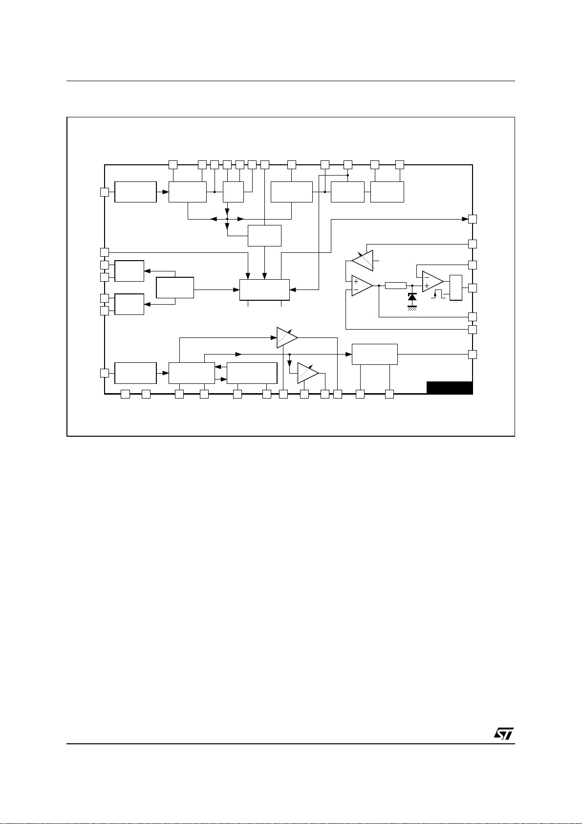
The goal of this IC is to control all the functions
related to the horizontal and vertical deflection in a
multimodes or multisync monitor.
As can be seen in the block diagram, the
STV7778S includes the following functions :
- Positive or Negative sync polarities,
- Auto-sync horizontal processing,
- H-PLL lock/unlock identification,
- Auto-sync Ver tical processing,
- East/West signal processing block,
- B+ controller,
- Safety blanking output.
An internal metal shield give to the STV7778S more
immunity against electromagnetic and electrostatic
fields, and therefore, additional safety for critical
applications (for example, in case of CRTs with
small coated area).
EWPCC
.
VERTICAL PARABOLA GENERATOR WITH DC
CONTROLLED KEYSTONE AND AMPLITUDE
GENERAL
.
COMPARED WITH THE STV7778, THE
STV7778S HAS AN INTERNAL METAL SHIELD
PROTECTION AGA INST OVER VOLTAGE.
.
POS/NEG H AND V SYNC P O L
.
SEPARATED H AND V TTL INPUT
.
SAFETY BLAN KING OUT PUT
DESCRIPTION
The STV7778S is a monolithic integrated circuit
assembled in a 42 pins shrunk dual in line plastic
package.
September 1998
SHRINK42
(Plastic Package)
ORDER CODE : STV7778S
1/11
Page 2
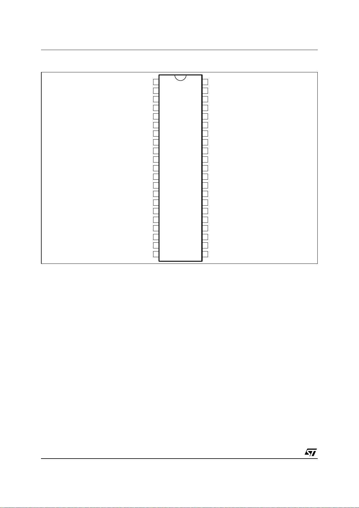
STV7778S
PIN CONNECTIONS
PLL2C
H-DUTY
HFLY
HGND
HREF
NC
NC
NC
NC
C0
R0
PLL1F
HLOCK-CAP
FH-MIN
H-POS
XRAY-IN
HSYNC
V
GND
H-OUTEM
H-OUTCOL
1
2
3
4
5
6
7
8
9
10
11
12
13
14
15
16
17
18
CC
19
20
21 22
42 I
41
40
39
38
37
36
35
34
33
32
31
30
29
28
27
26
25
24
23
SENSE
COMP
REGIN
B+-ADJ
KEYST
E/W-AMP
E/WOUT
PLL1INHIB
VSYNC
V-POS
V
DCOUT
V-AMP
VOUT
VS-CENT
VS-AMP
VCAP
V
REF
VAGCCAP
VDND
SBLKOUT
B+OUT
7778S-01.EPS
2/11
Page 3

STV7778S
PIN-OUT DESCRIPTION
Pin N° Name Function
1 PLL2C Second PLL Loop Filter
2 H-DUTY DC Control of Horizontal Drive Output Pulse Duty-cycle.
3 H-FLY Horizontal Flyback Input (Positive Polarity)
4 H-GND Horizontal Section Ground. Must be connected only to components related to H blocks.
5 H-REF Horizontal Section Reference Voltage. Must be filtered by capacitor to Pin 4
6NC
7NC
8NC
9NC
10 C0 Horizontal Oscillator Capacitor. To be connected to Pin 4.
11 R0 Horizontal Oscillator Resistor. To be connected to Pin 4.
12 PLL1F First PLL Loop Filter. To be connected to Pin 4.
13 HLOCK-CAP Firs t P L L L o ck / Un l oc k T i me C o ns tant Capacitor. Capacitor filtering the frequency change detected
14 FH-MIN
15 H-POS DC Control for Horizontal Centering
16 XRAY-IN X-RAY Protection Input (with internal latch function)
17 H-SYNC TTL Horizontal Sync Input
18 V
CC
19 GND Ground
20 H-OUTEM Horizontal Drive Output (emiter of internal transistor)
21 H-OUTCOL Horizontal Drive Output (open collector of internal transistor)
22 B+ OUT B+ PWM Regulator Output
23 SBLK OUT Safety Blanking Output. Activated duri ng frequency changes, when X-RAY input is triggere d or
24 VGND Vertical Section Signal Ground
25 VAGCCAP Memory Capacitor for Automatic Gain Control Loop in Vertical Ramp Generator
26 V
REF
27 VCAP Vertical Sawtooth Generator Capacitor
28 VS-AMP DC Control of Vertical S Shape Amplitude
29 VS-CENT DC Control of Vertical S Centering
30 VOUT Vertical Ramp Output (with frequency independant amplitude and S-correction)
31 V-AMP DC Control of Vertical Amplitude Adjustment
32 V
DCOUT
33 V-POS DC Control of Vertical Position Adjustment
34 VSYNC Vertical TTL Sync Input
35 PLL1INHIB TTL Input for PLL1 Output Current Inhibition (To be used in case of comp sync input signal)
36 E/WOUT East/West Pincushion Correction Parabola Output
37 E/W-AMP DC Control of East/West Pincushion Correction Amplitude
38 KEYST DC Control of Keystone Correction
39 B+ ADJ DC Control of B+ Adjustment
40 REGIN Regulation Input of B+ Control Loop
41 COMP B+ Error Amplifier Output for Frequency Compensation and Gain Setting
42 I
SENSE
If this pin is grounded, the horizontal and vertical outputs are inhibited. By connecting a capacitor
on this pin a soft-start function may be realized on h-drive output.
on Pin13. When frequency is changing, a blanking pulse is generated on Pin 23, the duration of this
pulse is proportionnal to the capacitor on Pin 13. To be connected to Pin 4.
DC Control for Free Running Frequency Setting. Comming from DAC output or DC voltage
generated by a resistor bridge connected between Pin 5 and 4.
Supply Voltage (12V Typical)
when VS is too low.
Vertical Section Reference Voltage
Vertical Position Reference Voltage Output Temperature Matched with V-AMP Output
Sensing of External B+ Switching Transistor Emiter Current
7778S-01.TBL
3/11
Page 4
STV7778S
BLOCK DIAGRAM
PLL1INHIB
35
H-POS
PLL1FR0C0
1112 131415 21
FH-MIN
HLOCK-CAP
HFLY
10
PLL2C
1 23
H-DUTY
H-OUTEM
20
H-OUTCOL
HSYNC
XRAY-IN
HREF
HGND
VREF
VGND
VSYNC
17
16
5
4
26
24
34
INPUT
INTERFACE
H-VREF
V-VREF
INPUT
INTERFACE
1819
GND
1st PHASE
COMP
BANDGAP
VERTICAL
OSCILLATOR
27 2829 30
CC
V
VCAP
VCO
LOCK
DETECT
SAFETY
PROCESSOR
V
CC
S
CORRECTION
25 31 3233
VAGCCAP
VS-CENT
2nd PHASE
COMP
Outputs
Inhibition
V-POS
VS-AMP
V-AMP
SHAPER
VOUT
PULSE
DCOUT
V
OUTPUT
BUFFER
V
REF
EA
PARABOLA
GENERATOR
3738
KEYST
E/W-AMP
R
S
STV7778S
23
39
42
22
41
40
36
SBLKOUT
B+-ADJ
I
SENSE
B+OUT
COMP
REGIN
E/WOUT
7778S-02.EPS
4/11
Page 5

STV7778S
ABSOLUTE MAX RATING
Symbol Parameter Value Unit
V
CC
V
IN
VESD ESD Succeptibility
T
stg
T
T
oper
THERMAL DATA
Symbol Parameter Value Unit
R
th (j-a)
HORIZONTAL SECTION
Operating conditions
Symbol Parameter Test conditions Min. Typ. Max. Unit
VCO
R0min Oscillator Resistor Min Value Pin 11 6 kΩ
C0min Oscillator Capacitor Min Value Pin 10 390 pF
Fmax Maximum Oscillator Frequency 70 kHz
HsVR Horizontal Sync Input Voltage Pin 17 0 5.5 V
INPUT SECTION
MinD Minimum Input Pulses Duration Pin 17 1 µS
Mduty Maximum Input Signal Duty Cycle Pin 17 25 %
OUTPUT SECTION
I3m Maximum Input Peak Current on Pin 3 2 mA
HOI1 Horizontal Drive Output Max Current Pin 20, sourced current 20 mA
HOI2 Horizontal Drive Output Max Current Pin 21, sunk current 20 mA
DC CONTROL VOLTAGES
DCadj DC Voltage Range on DC Controls V
Supply Voltage (Pin 18) 13.5 V
Max Voltage on Pins 2, 14, 15, 28, 29, 31, 33, 37, 38, 39
Pin 3
Pins 17, 34
Pin 40
Pin 42
Pin 16
Human Body Model, 100pF Discharge through 1.5kΩ
EIAJ Norm, 200pF Discharge through 0Ω
8
1.8
6
8
8
6
2
300
Storage Temperature -40, +150 °C
Max Operating Junction Temperature 150 °C
j
Operating Temperature 0, +70 °C
Junction-Ambient Thermal Resistance Max. 65 °C/W
= 8V, Pins 2-14-15 2 6 V
REF-H
V
kV
V
7778S-02.TBL
7778S-03.TBL
7778S-04.TBL
5/11
Page 6

STV7778S
HORIZONTAL SECTION
Electrical Characteristics
(continued)
(VCC = 12V, T
amb
= 25°C)
Symbol Parameter Test conditions Min. Typ. Max. Unit
SUPPLY AND REFERENCE VOLTAGES
V
I
V
REF-H
I
REF-H
V
REF-V
I
REF-V
Supply Voltage Pin 18 10.8 12 13.2 V
CC
Supply Current Pin 18, See Figure 1 40 60 mA
CC
Reference Voltage for Horizontal Section Pin 5 7.4 8 8.6 V
Max Sourced Current on V
REF-H
Pin 5 2 mA
Reference Voltage for Vertical Section Pin 26 7.4 8 8.6 V
Max Sourced Current on V
REF-V
Pin 26 2 mA
INPUT SECTION/PLL1
V
V
INTH
Hor Input Threshold Voltage Pin 17 Low level voltage
VCO Control Voltage V
VCO
High level voltage 2
= 8V, Pin 12 1.6 6.2 V
REF-H
0.8 V
VCOG VCO Gain, dF/dV Pin 12 R0 = 6.49kΩ, C0 = 680pF 15 kHz/V
Hph Horizontal Phase Adjustment (Pin 15) % of Hor period ±10 %
FFadj Free Running Frequency Adjustment (Pin 14) Without H-sync Signal ±20 %
CR PLL1 Capture Range (F0 = 27kHz)
Fh Min
Fh Max
See conditions on Figure 1
28 kHz
70
PLLinh PLL 1 Inhibition (Pin 35)
PLL ON
PLL OFF
V
35
V
35
2
0.8
SECOND PLL AND HORIZONTAL OUTPUT SECTION
FBth Flyback Input Threshold Voltage Pin 3 0.65 0.75 V
Hjit Horizontal Jitter 150 ppm
HDmin
HDmin
Minimum Hor Drive Output Duty-cycle
Maximum Hor Drive Output Duty-cycle
HDvd Horizontal Drive Low Level Output Voltage V
HDem Horizontal Drive High Level Output Voltage
(output on Pin 20)
Pin 20 or 21, V
Pin 20 or 21, V
, Iout = 20mA,
21-V20
Pin 20 to GND
Pin 21 to V
CC
= 2V
2
= 6V 453050
2
, I
= 20mA
OUT
9.5 10 V
35 %
1.1 1.7 V
XRAYth X-RAY Protection Input Threshold Voltage Pin 16 1.6 1.8 V
ISblkO Maximum Output Current on Safety Blanking
Output
VSblkO Low-Level Voltage on Safety Blanking Output V
Vphi2 Internal Clamping Voltage on 2nd PLL Loop Filter
Output (Pin 1)
V
Pin 2 Threshold Voltage to Stop H-out, V-out
OFF
B+out and to Activate S-BLK.OFF Mode when
V2 < V
OFF
I
23
with I23 = 10mA 0.25 0.5 V
23
Vmin
Vmax
V
2
10 mA
1.6
3.2
1V
V
kHz
V
%
V
V
7778S-05.TBL
6/11
Page 7

STV7778S
B+ SECTION
Operating Conditions
Symbol Parameter Test conditions Min. Typ. Max. Unit
EAOI Maximum Error Amplifier Output Current Sourced by Pin 41
Sunk by Pin 41
FeedRes Minimum Feedback Resistor Resistor between Pins 40
5kΩ
and 41
Electrical Characteristics
(VCC = 12V, T
amb
= 25°C)
Symbol Parameter Test conditions Min. Typ. Max. Unit
OLG Error Amplifier Open Loop Gain At low frequency
(see Note 1)
UGBW Unity Gain Bandwidth (see Note 1) 6 MHz
IRI Regulation Input Bias Current Current sourced by Pin 40
(PNP base)
EAOI Maximum Guaranted Error Amplifier
Output Current
Current sourced by Pin 41
Current sink by Pin 41
0.5
2
CSG Current Sense Input Voltage Gain Pin 42 3
MCEth Max Curent Sense Input Threshold Voltage Pin 42 1.2 V
ISI Current Sense Input Bias Current Current sunk by Pin 42
(NPN base)
Tonmax Maximum External Power Transistor on Time % of H-period,
@ f0 = 27kHz
B+OSV B+ Output Low Level Saturation Voltage V
IVref Internal Reference Voltage
V
REFADJ
Internal Reference Voltage Adjustment 2V < V39 < 6V ±14 %
with I22 = 10mA 0.25 V
22
On error amp (+) input for
= 4V
V
39
0.52mA
85 dB
0.2 µA
1 µA
75 %
4.9 V
mA
7778S-06.TBL
mA
mA
7778S-07.TBL
EAST WEST PARABOLA GENERA TOR
(V
Electrical Characteristics
= 12V, T
CC
Symbol Parameter Test conditions Min. Typ. Max. Unit
Vsym Parabola Symetry Adjustment Capability
(for Keystone Adjustment ; with Pin 38)
Kadj Keystone Adjustment Capability
B/A ratio
A/B ratio
Paramp Parabola Amplitude Adjustment Capability
Maximum Amplitude on Pin 36
Maximum Ratio between Max and Min
amb
= 25°C)
See Figure 2 ;
Internal voltage
V
= 2V
38
V38 = 4V
= 6V
V
38
See Figure 2 ; V
= 2V
V
38
V38 = 6V
= 4.3V, V28 = 2V
V
38
V37 = 2V
2V < V
37
< 6V
37
= 4V
3.2
3.5
3.8
2.3
2.0
3.3
3.834.3 V
2.4
V
7778S-08.TBL
7/11
Page 8

STV7778S
VERTIC AL SECTION
Operating Conditions
Symbol Parameter Test conditions Min. Typ. Max. Unit
VSVR Vertical Sync Input Voltage On Pin 34 0 5.5 V
Electrical Characteristics
(VCC = 12V, T
Symbol Parameter Test conditions Min. Typ. Max. Unit
I
BIASP
I
BIASN
Pin 23-28-29 Bias Current (Current sourced
by PNP base)
Pin 31 Bias Current (Current sunk by NPN
base)
VSth Vertical Sync Input Threshold Voltage
VSBI Vertical Sync Input Bias Current
(Current Sourced by PNP Base)
V
V
V
I
R27
Voltage at Ramp Bottom Point On Pin 27 2/8 V
RB
Voltage at Ramp Top Point (with Sync) On Pin 27 5/8 V
RT
Voltage at Ramp Top Point (without Sync) On Pin 27 VRT-0.1 V
RTF
Output Current Range on Pin 27 during Ramp
Charging Time. Current to Charge Capacitor
between Pin 27 and Ground
VSW Minimum Vertical Sync Pulse Width Pin 34 5 µS
VSmDut Vertical Sync Input Maximum Duty-cycle Pin 34 15 %
VSTD Vertical Sawtooth Discharge Time Duration On Pin 27, with 150nF cap 85 µS
VFRF Vertical Free Running Frequency (V
ASFR AUTO-SYNC Frequency (see Note 3) With C
RATD Ramp Amplitude Thermal Drift On Pin 30 (see Note 1),
RAFD Ramp Amplitude Drift Versus Frequency V
Rlin Ramp Linearity on Pin 27 ∆I
27/I27
Rload Minimum Load on Pin 25 for less than 1%
Vertical Amplitude Drift
Vpos Vertical Position Adjustment Voltage on
Pin 32
I
VPOS
Max Current on Vertical Position Control
Output (Pin 32)
Vor Vertical Output Voltage (on Pin 30)
(Peak to Peak Voltage on Pin 30)
V
OUTDC
DC Voltage on Vertical Output (Pin30) See Note 4 7/16 V
V0I Vertical Output Maximum Output Current On Pin 30 ±5mA
dVS Max Vertical S-Correction Amplitude
(V
= 2V Inhibits S-CORR; V28 = 6V gives
28
Maximum S-CORR) (see Figure 3)
Ccorr C-Correction Adjustment Range Voltage on
Pin 27 for Maximum Slope on the Ramp
(with S-Correction) (see Figure 4)
Notes :
1. These parameters are not tested on each unit. They are measured during our internal qualification procedure which includes
characterization on batches comming from corners of our processes and also temperature charac terization.
2. When 2V are applied on Pin 28 (Vertical S-Correction control), then the S-Correction is inhibited, consequently the sawtooth have
a linear shape.
3. It is the frequency range for which the VERTICAL OSCILLATOR will a uto mat ic al ly synchr o nize , using a single capacitor value on
Pin 27 and with a constant ramp amplitude.
4. Typically 3.5V for Vertical reference voltage typical value (8V).
= 25°C)
amb
For V
= 2V 2 µA
23-28-29
For V31 = 6V 0.5 µA
Pin 34; High-level
V
= 0.8V 1 µA
34
V28 = 2V (Note 2),
27
< 5V
2V < V
Min current
Max current 10015135
= 2V) Measured on Pin 27,
28
Cosc (Pin27) = 150nF
= 150nF ±5% 50 120 Hz
27
(0°C < T
31
50Hz < F < 120Hz
< 70°C)
amb
= 6V, C27 = 150nF,
V28 = 2V, V25 = X = 4.3V,
2.5V < V27 < 4.5V
V
= 2V
33
= 4V
V
33
V33 = 6V 3.65
= 2V
V
31
= 4V
V
31
V31 = 6V 3.75
∆V/V30pp at T/4
∆V/V30pp at 3T/4
V
= 2V
29
V29 = 4V
V
= 6V
29
Low-level
2
0.8
V
V
REF-V
REF-V
20 µA
µA
100 Hz
100 ppm/°C
200 ppm/Hz
0.5 %
50 MΩ
3.2
3.5
3.8
3.3 V
V
V
±2mA
2
2.2 V
3
4
-4
+4
3
3.5
4
V
V
REF-V
%
%
V
V
V
7778S-09.TBL
7778S-10.TBL
8/11
Page 9

STV7778S
Figure 1 :
Testing Circuit
W
S6 12V
4.7k
22nF
W
10k
12V
W
470pF
3.9k
22
42
R
S
W
W
47k
10k
36
40
41
W
4.7k
12V
23
39
STV7778S
REF
V
EA
BUFFER
OUTPUT
20
PULSE
SHAPER
1 23
PARABOLA
GENERATOR
3738
31 3233
COMP
10
1112 131415 21
35
2nd PHASE
VCO
COMP
1st PHASE
INPUT
INTERFACE
17
LOCK
DETECT
Outputs
Inhibition
SAFETY
CC
PROCESSOR
V
S
CORRECTION
470nF
1%
25
VERTICAL
27 2829 30
OSCILLATOR
BANDGAP
INPUT
H-VREF
4
5
16
F
m
2.2
26
V-VREF
24
F
m
2.2
INTERFACE
34
1819
1%
150nF
S512V
7778S-06.EPS
220nF
680pF
1%
6.49k
W
1.8k
W
4.7µF
10nF
9/11
Page 10

STV7778S
Figure 2 :
Figure 3 :
Keystone Adjustment
AB
S Amplitude Adjustment
V
30
V
36
V
= 2V
38
= 4V
V
38
V
= 6V
38
V
27
3.8
3.5
3.2
7778S-03.AI
∆V
V30pp
Figure 4 :
0 T/4 T/2 T3T/4
∆V increase when V28 increase.
∆V = 0 when V
C Correction Adjustment
V
4.0V
3.5V
3.0V
= 0.
28
27
0T
7778S-04.AI
7778S-0 5.AI
10/11
Page 11

PACKAGE MECHANICAL DATA
42 PINS - PLASTIC PA CK AGE
A2
A1
LA
STV7778S
E
E1
42
1
Dimensions
B eB1
D
22
21
c
SDIP42
Millimeters Inches
Min. Typ. Max. Min. Typ. Max.
e1
e2
E
.015
0,38
Gage Plane
e3
e2
A 5.08 0.200
A1 0.51 0.020
A2 3.05 3.81 4.57 0.120 0.150 0.180
B 0.36 0.46 0.56 0.0142 0.0181 0.0220
B1 0.76 1.02 1.14 0.030 0.040 0.045
c 0.23 0.25 0.38 0.0090 0.0098 0.0150
D 37.85 38.10 38.35 1.490 1.5 1.510
E 15.24 16.00 0.60 0.629
E1 12.70 13.72 14.48 0.50 0.540 0.570
e 1.778 0.070
e1 15.24 0.60
e2 18.54 0.730
e3 1.52 0.060
L 2.54 3.30 3.56 0.10 0.130 0.140
Information furnished is believed to be accurate and reliable. However, STMicroelectronics assumes no responsibility for the
consequences of use of such information nor for any infringement of patents or other rights of third parties which may result from
its use. No licence is granted by implication or otherwise under any patent or patent rights of STMicroelectronics. Specifications
mentioned in this publication are subject to change without notice. This publication supersedes and replaces all information
previously supplied. STMicroelectronics products are not authorized for use as critical components in life support devices or sys tem s
without express written approv al of STMi cr oelec troni cs.
The ST logo is a registered trademark of STMicroelectronics
© 1998 STMicroelectronics - All Rights Reserved
Purchase of I
Rights to use these components in a I
2
C Components of STMicroelectronics, conveys a license under the Philips I2C Pate n t .
2
the I
C Standard Specifications as defined by Phili ps.
2
C system, is granted provided that the system conforms to
STMicroelectronics GROUP OF COMPANIES
Australia - Brazil - Canada - China - France - Germany - Italy - Japan - Korea - Malaysia - Malta - Mexico - Morocco - The Neth erlands
Singapore - Spain - Sweden - Switzerland - Taiwan - Thailand - United Kingdom - U.S.A.
http://www.st.com
11/11
PMSDIP42.EPS
SDIP42.TBL
 Loading...