

Page 1
PLASMA DISPLAY PANEL DATA DRIVER
.
64 OUTPUTS PLASMA DISPLAY DRIVE R
.
170V ABSOLUTE MAXIMU M SUP PLY
.
5V SUPPLY FOR LOGIC
.
50/40mA SOURCE / SINK OUTPUT
.
60/60mA SOURCE / SINK OUTPUT DIODE
.
64-BIT SHIFT REGISTER (20MHz)
.
BLK, POLARITY AND H IZ CONT ROL
.
BCD TECHNOLOGY
.
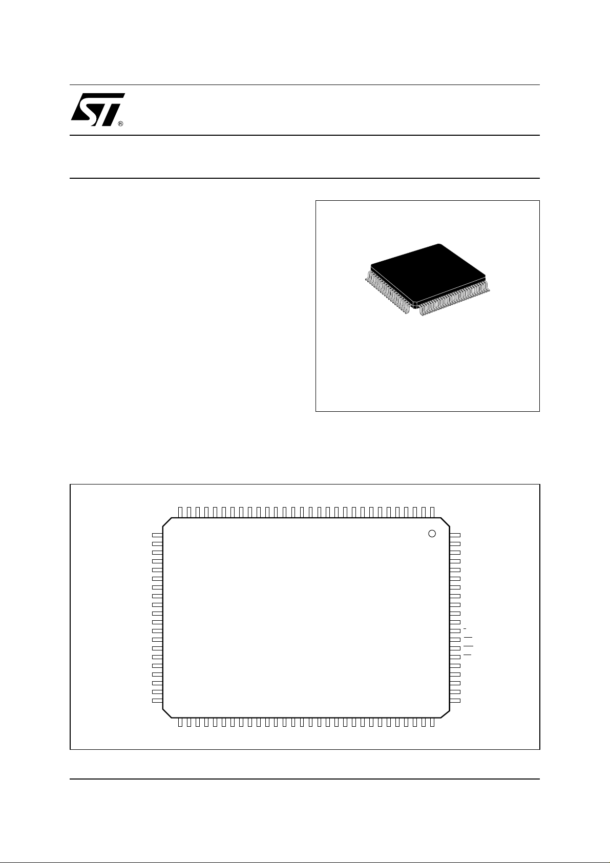
DIE or 100-PIN PQFP PACKAGE
DESCRIPTION
The STV7699 is a Plasma Display Panel (PDP)
data driver implemented in ST’s proprietary BCD
technology. Using a 4-bit wide cascadable shift
register, it drives 64 high current & high voltage outputs. By s erialy connecting s everal STV7699, any horizontal pixel definition can be performed. The 20MHz
shift clock gives an equivalent 80MHz shift register.
The STV7699 is supplied with a separated 170V
power out put s upply and a 5V logic supply.
STV7699
PRODUCT PREVIEW
PQFP100 (14 x 20 x 2.80mm)
(Full Plastic Quad Flat Pack)
ORDER CODE : STV7699
All command inputs are CMOS compatible.
The STV 7699 pack age is a 1 00-pin PQF P. It is als o
available as die.
PIN CONNECTIONS
SSP
V
OUT4
OUT5
OUT6
OUT7
987654321
SSP
V
OUT58
OUT59
OUT60
OUT61
OUT25
OUT26
OUT27
OUT28
V
OUT29
OUT30
OUT31
OUT32
V
V
SSSUB
OUT33
OUT34
OUT35
OUT36
V
OUT37
OUT38
OUT39
OUT40
PP
VPPV
OUT24
302928272625242322212019181716151413121110
31
32
33
34
35
SSP
36
37
38
39
40
SSP
41
42
43
44
45
46
SSP
47
48
49
50
5152535455565758596061626364656667686970717273747576777879
PP
VPPV
OUT41
SSP
V
OUT20
OUT22
OUT23
OUT21
OUT16
OUT17
OUT18
OUT19
STV7699
PQFP100
(Top View)
SSP
V
OUT42
OUT43
OUT44
OUT45
OUT46
OUT47
OUT48
OUT49
SSP
V
OUT12
OUT13
OUT14
OUT15
SSP
V
OUT50
OUT51
OUT52
OUT53
OUT8
OUT9
OUT10
OUT11
OUT54
OUT55
OUT56
OUT57
January 1999
This is advance information on a new product now in development or undergoing evaluation. Details are subject to change without notice.
PP
V
OUT1
OUT2
OUT3
100
99
98
97
96
95
94
93
92
91
90
89
88
87
86
85
84
83
82
81
80
PP
V
OUT62
OUT63
OUT64
V
A1
A2
A3
A4
CLK
STB
V
V
V
V
F/R
BLK
POL
HIZ
B4
B3
B2
B1
V
CC
SSLOG
SSLOG
SSLOG
SSLOG
SSSUB
7699-01.EPS
1/9
Page 2
STV7699
PIN ASSIGNMENT
(PQFP100)
Pin Number Symbol Type Function
100 V
1 - 29 - 30 - 51 - 52 - 80 V
6 - 15 - 24 - 35 - 40
46 - 57 - 66 - 75
90 to 93 V
41 - 81 V
2 to 5 - 7 to 14 - 16 to 23
25 to 28 - 31 to 34 - 36 to 39
42 to 45 - 47 to 50 - 53 to 56
58 to 65 - 67 to 74 - 76 to 79
95 CLK Input Clock of data shift register
94 STB Input Latch of data to outputs
88
87
86 HIZ Input Power Output High Impedance Control
89 F/R Input Selection of shift direction
96 to 99 A4 to A1 Input
82 to 85 B1 to B4 Output
CC
PP
V
SSP
SSLOG
SSSUB
Supply 5V Logic Supply
Supply High Voltage Supply of power outputs
Ground Ground of power outputs
Ground Logic Ground
Ground Substrate Ground
OUT1 to OUT 64 Output Power Output
Low to High transition makes the data enter into the shift
register and available at the output stage and at the output
of the shift register.
When the STB signal is set to low level, data are transferred
into the latch stage. When STB is set at high level, data are
held in the latch stage.
BLK Input Power Output Blanking Control
POL Input Power Output Polarity Control
Shift register data input and output according to
When set to low, Ai = input and Bi = output.
F/R value.
7699-01.TBL
PIN ASSIGNMENT
(Power Outputs)
Output N° Pin N° Output N° Pin N° Output N° Pin N° Output N° Pin N°
1 2 17 20 33 42 49 62
2 3 18 21 34 43 50 63
3 4 19 22 35 44 51 64
4 5 20 23 36 45 52 65
5 7 21 25 37 47 53 67
6 8 22 26 38 48 54 68
7 9 23 27 39 48 55 69
8 10242840505670
9 11253141535771
10 12 26 32 42 54 58 72
11 13 27 33 43 55 59 73
12 14 28 34 44 56 60 74
13 16 29 36 45 58 61 76
14 17 30 37 46 59 62 77
15 18 31 38 47 60 63 78
16 19 32 39 48 61 64 79
7699-02.TBL
2/9
Page 3

STV7699
PAD DIMENSIONS
(in µm)
The reference is the center of the die (x = 0, y = 0).
LEFT SIDE from top to bottom
Name Center : X Center : Y Size : x Size : y
V
PP
OUT1 -1738.0 2703.0 90.0 75.0
OUT2 -1738.0 2570.5 90.0 75.0
OUT3 -1738.0 2411.0 90.0 75.0
OUT4 -1738.0 2228.5 90.0 75.0
V
SSP
OUT5 -1738.0 1952.0 90.0 75.0
OUT6 -1738.0 1813.5 90.0 75.0
OUT7 -1738.0 1631.0 90.0 75.0
OUT8 -1738.0 1453.0 90.0 75.0
OUT9 -1738.0 1235.5 90.0 75.0
OUT10 -1738.0 1046.5 90.0 75.0
OUT11 -1738.0 862.0 90.0 75.0
OUT12 -1738.0 712.5 90.0 75.0
V
SSP
OUT13 -1738.0 431.0 90.0 75.0
OUT14 -1738.0 293.0 90.0 75.0
OUT15 -1738.0 82.5 90.0 75.0
OUT16 -1738.0 -109.5 90.0 75.0
OUT17 -1738.0 -277.0 90.0 75.0
OUT18 -1738.0 -471.0 90.0 75.0
OUT19 -1738.0 -691.5 90.0 75.0
OUT20 -1738.0 -822.5 90.0 75.0
V
SSP
OUT21 -1738.0 -1096.0 90.0 75.0
OUT22 -1738.0 -1335.5 90.0 75.0
OUT23 -1738.0 -1569.0 90.0 75.0
OUT24 -1738.0 -1697.5 90.0 75.0
V
PP
-1738.0 2867.5 90.0 75.0
-1738.0 2093.0 90.0 75.0
-1738.0 566.0 90.0 75.0
-1738.0 -953.0 90.0 75.0
-1715.0 -2045.0 90.0 200.0
Right SIDE from bottom to top
Name Center : X Center : Y Size : x Size : y
V
PP
OUT41 1737.5 -1646.0 90.0 75.0
OUT42 1737.5 -1507.0 90.0 75.0
OUT43 1737.5 -1328.0 90.0 75.0
OUT44 1737.5 -1096.0 90.0 75.0
V
SSP
OUT45 1737.5 -822.5 90.0 75.0
OUT46 1737.5 -691.5 90.0 75.0
OUT47 1737.5 -471.0 90.0 75.0
OUT48 1737.5 -277.0 90.0 75.0
OUT49 1737.5 -109.5 90.0 75.0
OUT50 1737.5 82.5 90.0 75.0
OUT51 1737.5 293.0 90.0 75.0
OUT52 1737.5 431.0 90.0 75.0
VSSP 1737.5 566.0 90.0 75.0
OUT53 1737.5 712.5 90.0 75.0
OUT54 1737.5 862.0 90.0 75.0
OUT55 1737.5 1046.5 90.0 75.0
OUT56 1737.5 1235.5 90.0 75.0
OUT57 1737.5 1453.0 90.0 75.0
OUT58 1737.5 1631.0 90.0 75.0
OUT59 1737.5 1813.5 90.0 75.0
OUT60 1737.5 1952.0 90.0 75.0
V
SSP
OUT61 1737.5 2228.5 90.0 75.0
OUT62 1737.5 2411.0 90.0 75.0
OUT63 1737.5 2570.5 90.0 75.0
OUT64 1737.5 2703.0 90.0 75.0
V
PP
1600.5 -2087.0 90.0 200.0
1737.5 -953.0 90.0 75.0
1737.5 2093.0 90.0 75.0
1737.5 2873.5 90.0 75.0
BOTTOM SIDE from left to right
Name Center : X Center : Y Size : x Size : y
OUT25 -1443.5 -3077.0 75.0 90.0
OUT26 -1249.0 -3077.0 75.0 90.0
OUT27 -1049.5 -3077.0 75.0 90.0
OUT28 -889.0 -3077.0 5.0 90.0
V
SSP
OUT29 -614.0 -3077.0 75.0 90.0
OUT30 -467.5 -3077.0 75.0 90.0
OUT31 -332.0 -3077.0 75.0 90.0
OUT32 -186.5 -3077.0 75.0 90.0
V
SSP
V
SSSUB
OUT33 209.5 -3077.0 75.0 90.0
OUT34 342.5 -3077.0 75.0 90.0
OUT35 467.5 -3077.0 75.0 90.0
OUT36 607.5 -3077.0 75.0 90.0
V
SSP
OUT37 892.5 -3077.0 75.0 90.0
OUT38 1045.5 -3077.0 75.0 90.0
OUT39 1252.0 -3077.0 75.0 90.0
OUT40 1433.5 -3077.0 75.0 90.0
-753.0 -3077.0 75.0 90.0
-54.0 -3077.0 75.0 90.0
78.0 -3077.0 75.0 90.0
752.0 -3077.0 75.0 90.0
TOP SIDE from right to left
Name Center : X Center : Y Size : x Size : y
V
SSSUB
B1 1478.5 3073.5 75.0 90.0
B2 1228.5 3077.0 75.0 90.0
B3 978.5 3077.0 75.0 90.0
B4 847.5 3077.0 75.0 90.0
HIZ 716.5 3077.0 75.0 90.0
POL 486.5 3077.0 75.0 90.0
BLK 355.5 3077.0 75.0 90.0
F/R 224.5 3077.0 75.0 90.0
V
SSLOG
V
SSLOG
STB -582.0 3077.0 75.0 90.0
CLK -713.0 3077.0 75.0 90.0
A4 -844.0 3077.0 75.0 90.0
A3 -975.0 3077.0 75.0 90.0
A2 -1106.0 3077.0 75.0 90.0
A1 -1471.5 3077.0 75.0 90.0
V
CC
1628.5 3073.5 75.0 90.0
31.0 3077.0 200.0 90.0
-354.5 3077.0 200.0 90.0
-1629.0 3077.0 75.0 90.0
3/9
Page 4

STV7699
BLOCK DIAGRAM
CLK
STB
BLK
POL
HIZ
95
99
94
88
87
86
STV7699
16-BIT SHIFT REGISTER
P1 P61
16-BIT SHIFT REGISTER
P2 P62
16-BIT SHIFT REGISTER
P3 P63
16-BIT SHIFT REGISTER
P4 P64
P64P1
Q1 Q64Q2 Q63
2 79
OUT1 OUT64
LATCH
P63P4
89
F/R
82
B1A1
8398
B2A2
8497
B3A3
8596
B4A4
100
V
CC
V
SSLOG
Pins 90 to 93
V
SSSUB
Pins 41-81
V
SSP
Pins 6-15-24-35
40-46-57-66-75
V
PP
Pins 1-29-30
51-52-80
7699-02.EPS
CIRCUIT DESCRIPTION
The STV7699 contains all the logic and the power
circuits necessary to drive the colums of a Plasma
Display Panel (P .D.P.). Data are shifted at each low
to high transition of the (CLK) shift clock. Data are
input in a 4-bit wide data bus to A 1 - A 4 input (case
of forward shift mode ;
F/R = low). After 16 shifts,
the first nibble is available at the serial outputs
B1 - B4. These outputs can be used to cascade
several drivers to performed any horizontal resolution. CLK, Ai and Bi inputs are Sm ith trigger inputs
to improve the noise margin.
The
Forward /Reverse (F/R) input is used to select
the direction of the shift register.
The maximum frequency of the shift clock is
20MHz.
All the output data are held and mem orized into the
latch stage when the Latch input (STB) is high.
When it is at low level, data are transferred from
the shift register to the latch and to the output power
stage.
Output state can be forced to high impedance by
pulling low
When
level or high level according to
HIZ input.
BLK is Low, all t he outputs are forced to low
POL signal value.
Output state copy data that was input, with the
4/9
same polarity, when
SSLOG
, V
SSSUB
V
BLK, HIZ and POL are High.
and V
are not internally con-
SSP
nected.
V
SSLOG
and V
must be connected as close as
SSSUB
possible to the logical reference ground of the
application.
Table 1 :
Data STB POL BLK HIZ
Note 1 :
Power Output Truth Table
Driver
Output
xxxxL
HIZ High impedance
x x L x H L Forced to low
x x H L H H Forced to high
x H H H H Qn (1) Latched data
L L H H H L Copy data
H L H H H H Copy data
Qn is the value memorised in the latch stage ; it is the value
of the parallel shift register output stage after n Clock
pulses.
Comments
A data loaded in the shift register is read on the
output power stage without inversion of its polarity .
Table 2 :
Control Table
F/R Ai Bi Comments
L Input Output Forward shift
H Output Input Reverse shift
Page 5

STV7699
ABSOLUTE MAXIMUM RATINGS
Symbol Parameter Value Unit
V
V
V
V
I
POUT
I
DOUT
T
T
T
THERMAL DATA
Symbol Parameter Value Unit
R
P
T
Notes :
Logic Supply -0.3, +7 V
CC
V
Logic Input Voltage -0.3, VCC + 0.3 V
IN
Logic Output Voltage -0.3, VCC + 0.3 V
OUT
Driver Output Voltage -0.3, +170 V
POUT
Driver Power Supply -0.3, +170 V
PP
Driver Output Current (2) ±60 mA
Diode Output Current (2) +40/-50 mA
Junction Temperature +150 °C
jmax
Operating Temperature -20, +85 °C
oper
Storage Temperature -50, +150 °C
stg
Junction-ambient Thermal Resistance (1) Max. 50 °C/W
th(j-a)
Operating Power Dissipation (T
oper
Operating Junction Temperature (1) Max. +125 °C
joper
1. For PQFP100 packaging.
2. Through all power outputs : with power dissipation lower or equal than P
= 25°C) Max. 2 W
amb
and junction temperature lower or equal than T
tot
jmax
7699-03.TBL
7699-04.TBL
.
ELECTRICAL CHARACTERISTICS
= 5V, VPP = 160V, V
(V
CC
SSP
= 0V, V
SSLOG
= 0V, V
SSSUB
= 0V , T
= 25°C, f
amb
= 20MHz,
CLK
unless otherwise specified)
Symbol Parameter Test Conditions Min. Typ. Max. Unit
SUPPLY
V
I
I
V
I
OUTPUT
OUT1-OUT64
V
POUT H
V
POUTL
V
DOUTH
V
DOUTL
I
OUTHIZ
SHIFT REGISTER OUTPUT (Ai or Bi according to F/R Status)
V
V
INPUT (CLK, STB,
V
Notes :
Logic Supply Voltage 4.5 5 5.5 V
CC
Logic Supply Current - - 100 µA
CCH
Logic Supply Current f
CCL
Power Output Supply Voltage - - 160 V
PP
Power Output Supply Current (steady outputs) - - 100 µA
PPH
Power Output High Level I
Power Output Low Level I
Output Diode High Level I
Output Diode Low Level I
= 20MHz - 12 TBD mA
CLK
= - 10mA, V
POUTH
I
= - 40mA, V
POUTH
= + 10mA
POUTL
I
= + 30mA
POUTL
= + 25mA (3)(4) - - 3 V
DOUTH
= - 25mA (3)(4) - - -3 V
DOUTL
PP
PP
= 65V
= 65V
55
TBD
-
-
60
-
-
-
2
125TBDVV
Output Stage Leakage Current on HIZ State - - ±10 µA
Logic Output High Level IOH = - 0.5mA 4 - - V
OH
Logic Output Low Level IOL = + 0.5mA - 0.1 0.3 V
OL
BLK, HIZ, Ai, Bi)
Input High Level 0.8 V
IH
V
Input Low Level - - 0.2 V
IL
I
High Level Input Current VIH = V
IH
CC
--1µA
--V
CC
CC
IILLow Level Input Current VIL = 0V - - -1 µA
3. Compatible with power dissipation and T
4. See test diagram.
≤ 125°C.
joper
V
V
V
7699-05.TBL
5/9
Page 6

STV7699
AC TIMINGS REQUIREMENTS
= 4.5V to 5.5V, T
(V
CC
Symbol Parameter Min. Typ. Max. Unit
t
t
WHCLK
t
WLCLK
t
SDAT
t
HDAT
t
DSTB
t
t
t
t
t
Data Clock Period 50 - - ns
CLK
Duration of clock (CLK) pulse at high level 15 - - ns
Duration of clock (CLK) pulse at low level 15 - - ns
Set-up Time of data input before clock (low to high) transition 0 - - ns
Hold Time of data input after clock (low to high) transition 15 - - ns
Minimum Delay to latch (STB) after clock (low to high) transition 20 - - ns
Latch (STB) Low Level Pulse Duration 10 - - ns
STB
Blanking (BLK) Pulse Duration 100 - - ns
BLK
Polarity (POL) Pulse Duration 100 - - ns
POL
High Impedance (HIZ) Pulse Duration 100 - - ns
HIZ
Set-up Time of Forward/Reverse Signal before Clock (low to high) transition 100 - - ns
SFR
AC TIMING CHARACTERISTICS
= 5V , VPP = 65V , V
(V
CC
V
= 4.0V, VOL = 0.4V , CL = 10pF, unless otherwise specified)
OH
Symbol Parameter Min. Typ. Max. Unit
t
t
RDAT
t
FDAT
t
PHL1
t
PLH1
t
PHL2
t
PLH2
t
PHL3
t
PLH3
t
PHL4
t
PLH4
t
PHZ5
t
PLZ5
t
PZH5
t
PZL5
t
ROUT
t
FOUT
Notes : 5. See test diagram.
Data Clock Period 50 - - ns
CLK
Logical Data Output Rise Time - TBD 30 ns
Logical Data Output Fall Time - TBD 30 ns
Delay of logic data output (high to low transition) after clock (CLK) transition
Delay of logic data output (low to high transition) after clock (CLK) transition
Delay of power output change (high to low transition) after clock (CLK) transition
Delay of power output change (low to high transition) after clock (CLK) transition-Delay of power output change (high to low transition) after Latch (STB) transition
Delay of power output change (low to high transition) after Latch (STB) transition-Delay of power output change (high to low transition) to Blank ( B LK) or Polarity
(POL) transition
Delay of power output change (low to high transition) to Blank (
(POL) transition
Delay of power output change (high to Hi-Z transition) after high impedance (HIZ) (5)
Delay of power output change (low to Hi-Z transition) after high impedance (
Delay of power output change (Hi-Z to high transition) after high impedance (HIZ) (5)
Delay of power output change (Hi-Z to low transition) after high impedance (HIZ) (5)--
Power Output Rise Time (6) - - 150 ns
Power Output Fall Time (6) - - 150 ns
6. One output among 64, loading capacitor C
= -20 to +85°C, input signals max leading edge & trailing edge (tR, tF) = 10ns)
amb
SSP
= 0V , V
SSLOG
= 0V , V
= 50pF, other outputs at low level.
OUT
SSSUB
= 0V , T
amb
= 25°C, V
BLK) or Polarity
= 0.2VCC, V
ILMax.
HIZ) (5)--
-
4040TBD
TBD
TBD
TBD
TBD
--TBD
TBD
TBD
TBD
TBD
TBD
IHMin.
TBDnsns
120
120nsns
110
110nsns
100
100nsns
100
100nsns
100
100nsns
= 0.8VCC,
7613-06.TBL
7613-07.TBL
6/9
Page 7

STV7699
Figure 1 :
CLK
SIN
SOUT
STB
F/R
OUTn
POL
OUTn
HIZ
OUTn
AC Characteristics Waveform
t
WHCLK
50% 50% 50%
t
FDAT
90%
10%
t
RDAT
90%
10%
50% 50%
t
PLH4
90%
10%
t
STB
50%
t
PHL3
90%
10%
t
PLH3
t
ROUT
90%
10%
t
FOUT
t
CLK
t
WLCLK
t
SDAT
t
HDAT
50% 50%
t
PHL1
50%
t
PLH1
t
DSTB
t
SFR
50%
t
PHL2
90%
10%
t
t
POL
PLH2
t
PHL4
90%
10%
t
HIZ
50% 50%
t
PHZ5
90%
10%
t
PLZ5
50%
t
PZH5
90%
t
PZL5
"1"
"0"
"1"
"0"
"1"
"0"
"1"
"0"
"1"
"0"
"1"
"0"
"1"
"0"
"1"
"0"
"1"
"0"
"1"
10%
"0"
7699-03.EPS
7/9
Page 8

STV7699
INPUT/OUTPUT SCHEMATICS
Figure 2 :
F/R, BLK, POL, HIZ
(Pins 89, 88, 87, 86)
Figure 4 :
(Pins 96 to 99)
(Pins 82 to 85)
F/R, BLK, POL, HIZ
(Pins 41-81)
Ai, Bi
A4 to A1
B1 to B4
V
SSSUB
(Pins 41-81)
(Pins 90 to 93)
V
V
SSSUB
SSLOG
V
(Pin 100)
CC
V
SSLOG
(Pins 90 to 93)
(Pin 100)
V
CC
V
SSLOG
(Pins 90 to 93)
Figure 3 :
CLK, STB
CLK, STB
(Pins 95, 94)
V
SSSUB
7699-04.EPS
Figure 5 :
(Pins 1, 29, 30, 51, 52, 80)
(Pins 6, 15, 24, 35, 40, 46, 57, 66, 75)
7699-06.EPS
(Pins 41-81)
Power Output
V
PP
V
SSP
V
(Pin 100)
CC
V
SSLOG
(Pins 90 to 93)
OUTi
(Pins 2 to 5, 7 to 14, 16 to 23,
25 to 28, 31 to 34, 36 to 39,
42 to 45, 47 to 50, 53 to 56,
58 to 65, 67 to 74, 76 to 79)
7699-05.EPS
7699-07.EPS
8/9
Page 9

PACKAGE MECHANICAL DATA
100 PINS - PLASTIC QUAD FLA T PACK (PQFP)
80 51
81
STV7699
A
A2
e
E3
E1
SEATING PLANE
E
50
0,10 mm
.004 inch
A1
B
31
c
L1
L
K
Dimensions
100
130
D3
D1
D
Millimeters Inches
Min. Typ. Max. Min. Typ. Max.
A 3.40 0.134
A1 0.25 0.010
A2 2.55 2.80 3.05 0.100 0.110 0.120
B 0.22 0.38 0.0087 0.015
c 0 .13 0.23 0.005 0.009
D 22.95 23.20 23.45 0.903 0.913 0.923
D1 19.90 20.00 20.10 0.783 0.787 0.791
D3 18.85 0.742
e 0.65 0.026
E 16.95 17.20 17.45 0.667 0.67 7 0.687
E1 13 .90 14.00 14.10 0.547 0.551 0.555
E3 12.35 0.48 6
L 0.65 0.80 0.95 0.026 0.031 0.037
L1 1.60 0.063
K0
Information furnished is believed to be accurate and reliable. However, STMicroelectronics assumes no responsibility for the
consequences of use of such information nor for any infringement of patents or other rights of third parties which may result from
its use. No licence is granted by implication or otherwise under any patent or patent rights of STMicroelectronics. Specifications
mentioned in this publication are subject to change without notice. This publication supersedes and replaces all information
previously supplied. STMicroelectronics products are not authorized for use as critical components in life support devices or sys tem s
without express written approv al of STMi cr oelec troni cs.
Purchase of I
Rights to use these components in a I
Australia - Brazil - Canada - China - France - Germany - Italy - Japan - Korea - Malaysia - Malta - Mexico - Morocco - The Netherlands
Singapore - Spain - Sweden - Switzerland - Taiwan - Thailand - United Kingdom - U.S.A.
The ST logo is a registered trademark of STMicroelectronics
© 1999 STMicroelectronics - All Rights Reserved
2
C Components of STMicroelectronics, conveys a license under the Philips I2C Pate n t .
2
the I
C Standard Specifications as defined by Phili ps.
2
C system, is granted provided that the system conforms to
STMicroelectronics GROUP OF COMPANIES
http://www.st.com
o
(Min.), 7o (Max.)
9/9
PMPQF100.EPS
5F.TBL
 Loading...