

Page 1
This ispreliminary information on a new product indevelopment orundergoing evaluation. Details are subject tochange without notice.
Version 4.1
June 2000 1/17
STV7617, STV7617D, STV7617U
PLASMA DISPLAYPANEL SCAN DRIVER
FEATURE
■ 64/65 SELECTABLE OUTPUT PLASMA
DISPLAY DRIVER
■ 100 V ABSOLUTE MAXIMUM SUPPLY
■ 5 V SUPPLY FOR LOGIC
■ 100/850 mA SOURCE/SINK OUTPUT
■ 700 mA SOURCE/SINK OUTPUT DIODE
■ 65-bit BIDIRECTIONAL SHIFT REGISTER
(8 MHz)
■ HIGH IMPEDANCE OUTPUT CONTROL
■ BCD TECHNOLOGY
■ 100-PIN TQFP PACKAGE WITH
INTEGRATED HEATSINK
DESCRIPTION
The STV7617 is a scan driver for Plasma Display
Panel (PDP) implemented in ST’s proprietary
BCD technology. Using a 65-bit cascadable
8 MHz shift register, it drives 65 high current &
high voltage outputs.The STV7617 can beconfigured either in 64 or 65 outputs depending on the
SEL input Pin.
By serially connecting several STV7617, any vertical pixel definition can be performed. The
STV7617 is supplied with a separated 90V power
output supply and a 5 V logic supply. All command
inputs are CMOS compatible. The STV7617 package is a 100-pin TQFP with integrated heatsink located on the bottom (STV7617D) or top
(STV7617U) of the package. It is also available
without heatsink (STV7617).
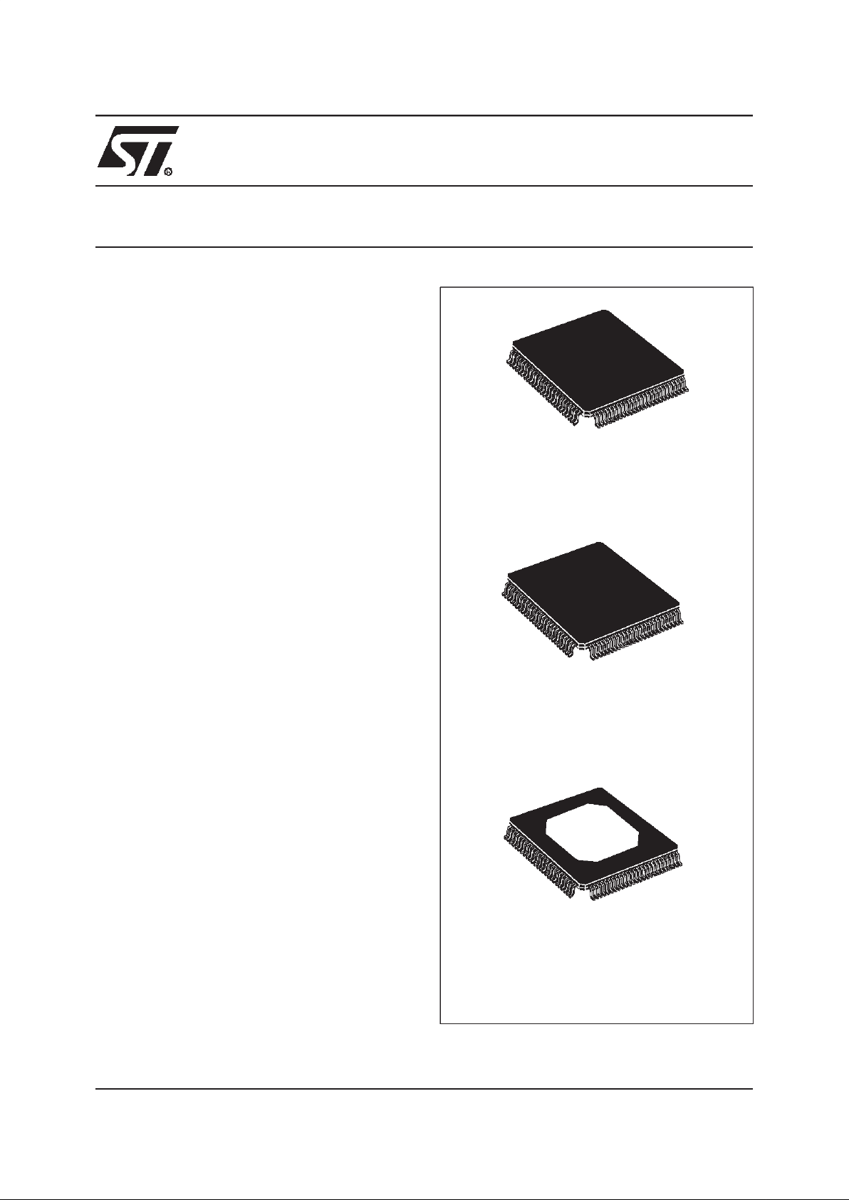
TQFP100 (14 x 14 x 1.4 mm Slug-down)
(Thin Plastic Quad Flat Pack)
ORDER CODE: STV7617D
TQFP100 (14 x 14 x 1.4 mm Slug-up)
(Thin Plastic Quad Flat Pack)
ORDER CODE: STV7617U
TQFP100 (14 x 14 x 1.4 mm)
(Thin Plastic Quad Flat Pack)
ORDER CODE: STV7617
1
Page 2

TABLE OF CONTENTS
2
2/17
PIN CONNECTIONS (SLUG-UP) . . . . . . . ............................................3
PIN CONNECTIONS (SLUG-DOWN) . . . ............................................ 4
PIN CONNECTIONS (NO SLUG) . . . ................................................ 5
PIN ASSIGNMENT . . . . . . . . . . . . . . . . . . . . . ......................................... 6
BLOCK DIAGRAM .............................................................. 7
CIRCUIT DESCRIPTION . . . . . . . . . . . . . . . . . . . . . . . .................................. 7
ABSOLUTE MAXIMUM RATINGS ................................................. 8
THERMAL DATA . . . . . . . . . . . . . . . ................................................ 8
ELECTRICAL CHARACTERISTICS . . . . . . . . . . . . . ...................................9
AC TIMING REQUIREMENTS . . . . . . . . . . . . . . . . . . . . . . . . . ........................... 10
AC TIMING CHARACTERISTICS . . . . . . ........................................... 10
INPUT/OUTPUT CHARACTERISTICS . . . . . . . . . . . . . . . . . . . . . . . . . . . . . . . . . . . . . . . . . . . . . 13
PACKAGE MECHANICAL DATA (SLUG-DOWN) . . . . . . . . . . . . . . . . . . . . . . . . . . . . ........ 14
PACKAGE MECHANICAL DATA (SLUG-UP) . . . . . . . . . . . . . . . . . . . . . . . . . . . . ...........15
PACKAGE MECHANICAL DATA (NO SLUG) . . . .................................... 16
2
Page 3

STV7617, STV7617D, STV7617U
3/17
PIN CONNECTIONS (SLUG-UP)
(TQFP100 Slug-up)
1
2
3
4
5
6
7
8
9
10
11
12
13
14
15
16
17
18
19
20
21
22
23
24
25
75
74
73
72
71
70
69
68
67
66
65
64
63
62
61
60
59
58
57
56
55
54
53
52
51
26272829303132333435363738394041424344454647484950
100
9998979695949392919089888786858483828180797877
76
OUT63
OUT62
OUT61
OUT60
OUT59
OUT58
OUT57
OUT56
OUT55
OUT54
OUT33
OUT52
OUT51
OUT50
OUT49
OUT48
OUT47
OUT46
OUT45
OUT44
OUT43
OUT42
OUT41
OUT40
OUT39
OUT3
OUT4
OUT5
OUT6
OUT7
OUT8
OUT9
OUT10
OUT11
OUT12
OUT13
OUT14
OUT15
OUT16
OUT17
OUT18
OUT19
OUT20
OUT21
OUT22
OUT23
OUT24
OUT25
OUT26
OUT27
OUT28
OUT29
OUT30
NC
V
SSPVSSP
V
SSP
NC
VPPV
PP
OUT31
OUT32
OUT33
OUT34
OUT35
VPPVPPNC
V
SSSUB
V
SSPVSSP
NC
OUT36
OUT37
OUT38 OUT64
OUT65
VPPVPPNC
V
SSP
V
SSP
V
SSLOG
F/R
SOUT
CLK
STB
VCCBLK
HIZ
SIN
SEL
V
SSLOG
V
SSP
V
SSP
NC
VPPV
PP
OUT1
OUT2
STV7617U
TQFP100
(Top View)
3
Page 4
STV7617, STV7617D, STV7617U
4/17
PIN CONNECTIONS (SLUG-DOWN)
(TQFP100 Slug-down)
1
2
3
4
5
6
7
8
9
10
11
12
13
14
15
16
17
18
19
20
21
22
23
24
25
75
74
73
72
71
70
69
68
67
66
65
64
63
62
61
60
59
58
57
56
55
54
53
52
51
26272829303132333435363738394041424344454647484950
100
9998979695949392919089888786858483828180797877
76
OUT63
OUT62
OUT61
OUT60
OUT59
OUT58
OUT57
OUT56
OUT55
OUT54
OUT33
OUT52
OUT51
OUT50
OUT49
OUT48
OUT47
OUT46
OUT45
OUT44
OUT43
OUT42
OUT41
OUT40
OUT39
OUT3
OUT4
OUT5
OUT6
OUT7
OUT8
OUT9
OUT10
OUT11
OUT12
OUT13
OUT14
OUT15
OUT16
OUT17
OUT18
OUT19
OUT20
OUT21
OUT22
OUT23
OUT24
OUT25
OUT26
OUT27
OUT28
OUT29
OUT30
NC
V
SSPVSSPVSSP
NC
VPPV
PP
OUT31
OUT32
OUT33
OUT34
OUT35
V
PPVPP
NC
V
SSSUB
V
SSPVSSP
NC
OUT36
OUT37
OUT38 OUT64
OUT65
V
PPVPP
NC
V
SSP
V
SSP
V
SSLOG
F/R
SOUT
CLK
STB
VCCBLK
HIZ
SIN
SEL
V
SSLOG
V
SSP
V
SSP
NC
VPPVPPOUT1
OUT2
STV7617D
TQFP100
(Top View)
3
Page 5
STV7617, STV7617D, STV7617U
5/17
PIN CONNECTIONS (NO SLUG)
(TQFP100)
1
2
3
4
5
6
7
8
9
10
11
12
13
14
15
16
17
18
19
20
21
22
23
24
25
75
74
73
72
71
70
69
68
67
66
65
64
63
62
61
60
59
58
57
56
55
54
53
52
51
26272829303132333435363738394041424344454647484950
100
9998979695949392919089888786858483828180797877
76
OUT63
OUT62
OUT61
OUT60
OUT59
OUT58
OUT57
OUT56
OUT55
OUT54
OUT33
OUT52
OUT51
OUT50
OUT49
OUT48
OUT47
OUT46
OUT45
OUT44
OUT43
OUT42
OUT41
OUT40
OUT39
OUT3
OUT4
OUT5
OUT6
OUT7
OUT8
OUT9
OUT10
OUT11
OUT12
OUT13
OUT14
OUT15
OUT16
OUT17
OUT18
OUT19
OUT20
OUT21
OUT22
OUT23
OUT24
OUT25
OUT26
OUT27
OUT28
OUT29
OUT30
NC
V
SSPVSSPVSSP
NC
VPPV
PP
OUT31
OUT32
OUT33
OUT34
OUT35
VPPVPPNC
V
SSSUB
V
SSPVSSP
NC
OUT36
OUT37
OUT38 OUT64
OUT65
VPPVPPNC
V
SSP
V
SSP
V
SSLOG
F/R
SOUT
CLK
STB
VCCBLK
HIZ
SIN
SEL
V
SSLOG
V
SSP
V
SSP
NC
VPPVPPOUT1
OUT2
TQFP100
(Top View)
STV7617
3
Page 6

STV7617, STV7617D, STV7617U
6/17
PIN ASSIGNMENT
(TQFP100)
PIN ASSIGNMENT (Power Outputs)
Pin Number
Symbol Type Function
TQFP100 Slug-up
TQFP100 Slug-down/
TQFP100 No slug
88 88 V
CC
Supply 5 V Logic Supply
34-35-41-42
78-79-97-98
34-35-41-42
78-79-97-98
V
PP
Supply High Voltage Supply of power outputs
30-31-44-45
46-81-82-94-95
30-31-32-45
46-81-82-94-95
V
SSP
Ground Ground of power outputs
83-93 83-93 V
SSLOG
Ground Logic Ground
32 44 V
SSSUB
Ground Substrate Ground
77 to 48, 40 to 36,
28 to 1, 100-99
99-100, 1 to 28,
36 to 40,48 to 77
OUT1 to OUT65 Output Power Output
91 85 SOUT (SIN) Output Shift Register Data Output
90 86 CLK Input Clock of data shift register
89 87 Input Latch of data to outputs
87 89 BLK Input Power Output Blanking Control
86 90 Input Power Output High Impedance Control
85 91 SIN (SOUT) Input Shift Register Data Input
84 92 SEL Input Selection of number of power outputs
92 84 F/ Input Selection of shift direction
29-33-43-47-80-96 29-33-43-47-80-96 NC - Not connected
STB
HIZ
R
Output
Number
Pin Number
Output
Number
Pin Number
Output
Number
Pin Number
Slug-down/
No slug
Slug-up
Slug-down/
No slug
Slug-up
Slug-down/
No slug
Slug-up
1 7799 235521 451957
2 76 100 24 54 22 46 18 58
3 75 1 25 53 23 47 17 59
4 74 2 26 52 24 48 16 60
5 73 3 27 51 25 49 15 61
6 72 4 28 50 26 50 14 62
7 71 5 29 49 27 51 13 63
8 70 6 30 48 28 52 12 64
9 69 7 31 40 36 53 11 65
10 68 8 32 39 37 54 10 66
11 67 9 33 38 38 55 9 67
12 66 10 34 37 39 56 8 68
13 65 11 35 36 40 57 7 69
14 64 12 36 28 48 58 6 70
15 63 13 37 27 49 59 5 71
16 62 14 38 26 50 60 4 72
17 61 15 39 25 51 61 3 73
18 60 18 40 24 52 62 2 74
19 59 17 41 23 53 63 1 75
20 58 18 42 22 54 64 100 76
21 57 19 43 21 55 65 99 77
22 56 20 44 20 56
3
Page 7

STV7617, STV7617D, STV7617U
7/17
BLOCK DIAGRAM
CIRCUIT DESCRIPTION
The STV7617 contains all the logic and the power
circuits necessary to drive rows of a Plasma Display Panel (PDP). Data is shifted at each low to
high transition of the (CLK) shift clock. After 64 or
65 shifts (depending on SEL) the first bit presented
at (SIN) is available at the serial output (SOUT).
This output can be used to cascade several drivers to perform any vertical resolution. CLK, STB,
SIN and SOUT inputs are Smith trigger inputs.
BLK and HIZ logical inputs are internally pulled to
level ”1”. The maximum frequency of the shift
clock is 8 MHz.
Shift register outputs (P1, ... P65) are transferred
from theshiftregister into the latch stage when the
latch input (STB) isat low level.
Table1 : Output State Configuration
Sustain current must not besunkin the power outputs to VPP when the power supply is applied and
output state is in HIZ or at high state. V
SSSUB
and
V
SSLOG
mustbe connected as close as possible to
the logical reference ground of the application.
Table 2 : Shift Register Truth Table
Table 3 : Power Output Configuration
P1 P65
LATCH
Q1 Q65Q2 Q64
S65S1
V
SSP
V
PP
V
CC
V
SSLOG
SOUT (SIN)
SIN (SOUT)
STB
BLK
HIZ
OUT1 OUT65
STV7617
CLK
V
PP
V
SSP
V
PP
V
SSP
V
CC
V
CC
V
SSSUB
OUT64
65-BIT SHIFT REGISTER
SEL
F/R
SWITCH
STB BLK HIZ OutputState
* L L High impedance
LLH
Inverted copy of input
data
H L H Data latched
* H L Low level
* H H High Level
F/R CLK SIN SOUT Comments
H Rise In Out Forward Shift
H L or H In Out Steady
L Rise Out In Reverse Shift
L L or H Out In Steady
SEL F/R
Number of
Outputs
Comments
LL 64
Out 1 is in Hi-Z mode (outputs 65 to 2 powered)
LH 64
Out 65 is in Hi-Z mode (out-
puts 1 to 64 powered)
H L 65 Out 65 to Out 1 powered
H H 65 Out 1 to Out65 powered
3
Page 8

STV7617, STV7617D, STV7617U
8/17
ABSOLUTE MAXIMUM RATINGS
* In case of STV7617D
THERMAL DATA
Note 1 For TQFP100 packaging and slug soldered on printed circuit board.
Note 2 Through one power output.
Note 3 Through all power outputs (see test diagram): with Power dissipation lower or equal than Ptot and Junction tem-
perature lower or equal than T
jmax
and V
PP =VSSP.
Note 4 These parameters are measured during ST’s internal qualification which includes temperature characterisation
on standard batches and on corners batches of the process. These parameters are not tested on the parts.
Note 5 TQFP soldered on 4 layers Printed Circuit Board.
Symbol Parameter Value Unit
V
CC
Logic Supply (Pin88)* -0.3, +7 V
OUTi OutputPins (1 to 28, 36 to 40, 48 to 77, 99, 100) -0.3, +100 V
V
IN
Logic Input Voltage (Pins 84, 86, 87, 89, 90, 91, 92)* -0.3, VCC+0.3 V
V
OUT
Logic Output Voltage (Pin 85)
*
-0.3, VCC+ 0.3 V
V
POUT
Driver Output Voltage (scanning mode) -0.3, +100 V
I
POUT
Driver Output Current (1) (4) -100, +1 A mA
I
DOUT
Diode Output Current (3) (4) ±700 mA
T
jmax
Junction Temperature +150 °C
T
oper
Operating Temperature -20, +85 °C
T
stg
Storage Temperature -20, +150 °C
Symbol Parameter Value Unit
R
th(j-a)
Junction-ambient Thermal Resistance (1) 20 °C/W
T
joper
Maximum Operating Junction (1) 125 °C
R
th(j-a)
Junction-ambient Thermal Resistance (5) 40 °C/W
3
Page 9

STV7617, STV7617D, STV7617U
9/17
ELECTRICAL CHARACTERISTICS
(VCC=5V,VPP=90V,V
SSP
=0V,V
SSLOG
=0V,V
SSSUB
=0V,T
amb
=25°C, f
CLK
= 8 MHz, unless
otherwise specified)
Note 6 Peak current - Pulse mode 720 Hz - 0.2%. Duty cycle - VCC= 5.5 V ± 0.2 V.
Note 7 Compatible with power dissipation and T
joper
≤ 125°C.
Note 8 See test diagram page 12.
Symbol Parameter Test Conditions Min. Typ. Max. Unit
SUPPLY
V
CC
Logic Supply Voltage 4.5 5 5.5 V
I
CCH
Logic Supply Current - - 100 µA
I
CCL
Logic Supply Current
f
CLK
= 8 MHz
-5-mA
V
PP
Power Output Supply Voltage 20 - 90 V
I
PPH
Power Output Supply Current
(steady outputs)
--100µA
OUTPUT
OUT1-OUT65
V
POUTH
Power Output High Level
I
POUTH
=-20mA
83 86 - V
V
POUTH
Power Output High Level
I
POUTH
= - 15mA, VPP=40V
30 33 - V
V
POUTL
Power Output Low Level
I
POUTL
= + 400 mA
- 2.5 5 V
V
POUTL-P
Power Output Low Level-pulsed mode
I
POUTL-P
= 850 mA (6)
- - 15 V
V
DOUTH
Output Diode High Level
I
DOUTH
= +400 mA (7) (8)
- 1.7 5 V
V
DOUTL
Output Diode Low Level
I
DOUTL
= - 400 mA (7)(8)
- -1.2 -5 V
SOUT
V
OH
Logic Output High Level
I
OH
=-1mA
4 4.2 - V
V
OL
Logic Output Low Level
I
OL
=+1mA
- 0.1 0.4 V
INPUT (CLK, STB, BLK, HIZ, SIN, SEL)
V
IH
Input High Level
0.8 V
CC
--V
V
IL
Input Low Level - -
0.2V
CC
V
I
IH
High Level Input Current
V
IH=VCC
--10µA
I
IL
Low Level Input Current
CLK, SIN, STB, SEL,
BLK, HIZ
VIL=0V
-
-
-
-
-10
-40
µA
µA
3
Page 10

STV7617, STV7617D, STV7617U
10/17
AC TIMING REQUIREMENTS
(VCC=4.5 Vto 5.5 V,T
amb
= -20 to+85°C, input signalsmax leading edge & trailing edge (tR,tF) = 10 ns)
AC TIMING CHARACTERISTICS
(VCC=5V,VPP=90V,V
SSP
=0V,V
SSLOG
=0V,V
SSSUB
=0V,T
amb
=25°C, V
ILMax.
= 0.2 Vcc,
V
IHMin.
=0.8VCC,VOH= 4.0 V,VOL=0.4 V,unless otherwise specified)
Note 9 See test diagram page 12.
Note 10 One output among 64, loading capacitor C
OUT
= 200pF, other outputs at low level.
Symbol Parameter Min. Typ. Max. Unit
t
WHCLK
Duration of clock (CLK) pulse at high level 40 - - ns
t
WLCLK
Duration of clock (CLK) pulse at low level 40 - - ns
t
SDAT
Set-up Time of data input before clock (low to high) transition 10 - - ns
t
HDAT
Hold Time of data input after clock (low to high) transition 20 - - ns
t
DSTB
Minimum Delay to latch STB after clock (low to high) transition 25 - - ns
t
SSTB
Set-up Time STB before clock (low to high) transition 10 - - ns
t
STB
Latch STB Low Level Pulse Duration 20 - - ns
t
BLK
Blanking (BLK) Pulse Duration 500 - - ns
t
HIZ
High Impedance HIZ Pulse Duration 500 - - ns
Symbol Parameter Min. Typ. Max. Unit
t
CLK
Data Clock Period 125 - - ns
t
RDAT
Logical Data Output Rise Time - 12 20 ns
t
FDAT
Logical Data Output Fall Time - 10 20 ns
t
PHL1
t
PLH1
Delay of logic data output (high to low transition) afterclock (CLK) transition
(CL=10pF)
Delay of logic data output (low to high transition) after clock (CLK) transition
(CL=10 pF)
--37425060ns
ns
t
PHL2
t
PLH2
Delay of power output change (high to low transition) after clock (CLK) transition
Delay of power output change (low to high transition) after clock (CLK) transition
--110
115
180
180nsns
t
PHL3
t
PLH3
Delay of power output change (high to low transition) after Latch (STB) transition
Delay of power output change (low to high transition) after Latch (STB) transition
--8095165
165nsns
t
PHL4
t
PLH4
Delay of power output change (high to low transition) to blank (BLK) transition
Delay of power output change (low to high transition) to blank (BLK) transition
--7575160
160nsns
t
PHZ5
t
PLZ5
Delay of power output change (high to Hi-Z transition) after high impedance (HIZ)(9)
Delay of power output change (low to Hi-Z transition) after high impedance (HIZ)(9)--4080
160
160nsns
t
PZH5
t
PZL5
Delay of power output change (Hi-Z to high transition) after high impedance (HIZ) (9)
Delay of power output change (Hi-Z to low transition) after high impedance (HIZ) (9)--7540
160
160nsns
t
ROUT
Power Output Rise Time (10) - 175 350 ns
t
FOUT
Power Output Fall Time (10) - 35 150 ns
3
Page 11

STV7617, STV7617D, STV7617U
11/17
Figure 1: AC Characteristics Waveform
CLK
SIN
SOUT
STB
OUTn
HIZ (BLK = H)
OUTn
HIZ (BLK = L)
OUTn
t
WHCLK
t
CLK
t
WLCLK
t
SDAT
t
HDAT
t
PHL1
t
FDAT
t
RDAT
t
STB
t
DSTB
t
PHL3
t
PLH3
t
PHL2
t
PLH2
t
BLK/POL
t
PHL4
t
PLH4
t
HIZ
t
PHZ5
t
PZH5
t
ROUT
t
FOUT
50% 50% 50%
50% 50%
50% 50%
10%
90%
60%
40%
90%
10%
90%
10%
90%
10%
90%
10%
50% 50%
90%
10%
90%
10%
”1”
”0”
”1”
”0”
”1”
”0”
”1”
”0”
”1”
”0”
”1”
”0”
”1”
”0”
”1”
”0”
”1”
”0”
50%
90%
10%
t
PLH1
t
SSTB
50%
t
PLZ5
t
PZL5
3
Page 12

STV7617, STV7617D, STV7617U
12/17
Figure 2: Test Configuration
V
DOUTH
I
DOUTH
V
SSP
V
DOUTL
I
DOUTL
V
SSP
V
PP
=
V
SSP
V
PP
=VSSP
Output sinking current as positive value, sourcing current as negative value
V
DOUT
VPP/2
R
V
PP
OUT
3
Page 13

STV7617, STV7617D, STV7617U
13/17
INPUT/OUTPUT CHARACTERISTICS
Figure 3: BLK, HIZ Input
Figure 4: F/R, SEL, CLK, STB Input
Figure 5: SIN, SOUT Input
Figure 6: Power Output
BLK, HIZ
V
CC
V
CC
GNDLOG
GNDSUB
F/R, SEL
CLK, STB
V
CC
V
CC
GNDLOG
GNDSUB
SIN, SOUT
V
CC
V
CC
GNDLOG
GNDSUB
V
CC
V
PP
OUT 1
to O UT
6 5
V
SSP
3
Page 14

STV7617, STV7617D, STV7617U
14/17
PACKAGE MECHANICAL DATA (SLUG-DOWN)
100 PINS - THIN PLASTIC QUAD FLAT PACK (TQFP)
76100
50
D3
e
26
1
25
75
51
S1
H
S
c
B
A1
A2
A
D1
D
E3
E1
E
L
K
L1
0,25 mm
.010 inch
GAGE PLANE
0,075 mm
0.03 inch
SEATING PLANE
Dimensions
Millimeters Inches
Min. Typ. Max. Min. Typ. Max.
A 1.60 0.063
A1 0.05 0.15 0.002 0.006
A2 1.35 1.40 1.45 0.053 0.055 0.057
B 0.17 0.22 0.27 0.007 0.009 0.011
C 0.09 0.20 0.004 0.008
D 16.00 0.630
D1 14.00 0.551
D3 12.00 0.472
e 0.50 0.20
E 16.00 0.630
E1 14.00 0.551
E3 12.00 0.472
L 0.45 0.60 0.75 0.018 0.024 0.030
L1 1.00 0.039
K0°(Min.), 7° (Max.)
Slug Dimension For L/FramePad Size10.00 x 10.00 mm
H 9.85 0.388
S 8.80 0.346
S1 8.80 0.346
3
Page 15

STV7617, STV7617D, STV7617U
15/17
PACKAGE MECHANICAL DATA (SLUG-UP)
100 PINS - THIN PLASTIC QUAD FLAT PACK (TQFP)
76100
50
D3
e
26
1
25
75
51
S1
H
S
c
B
A1
A2
A
D1
D
E3
E1
E
L
K
L1
0,25 mm
.010 inch
GAGE PLANE
0,075 mm
0.03 inch
SEATING PLANE
Dimensions
Millimeters Inches
Min. Typ. Max. Min. Typ. Max.
A 1.60 0.063
A1 0.05 0.15 0.002 0.006
A2 1.35 1.40 1.45 0.053 0.055 0.057
B 0.17 0.22 0.27 0.007 0.009 0.011
C 0.09 0.20 0.004 0.008
D 16.00 0.630
D1 14.00 0.551
D3 12.00 0.472
e 0.50 0.20
E 16.00 0.630
E1 14.00 0.551
E3 12.00 0.472
L 0.45 0.60 0.75 0.018 0.024 0.030
L1 1.00 0.039
K0°(Min.), 7° (Max.)
Slug Dimension For L/FramePad Size10.00 x 10.00 mm
H 9.85 0.388
S 8.80 0.346
S1 8.80 0.346
3
Page 16

STV7617, STV7617D, STV7617U
16/17
PACKAGE MECHANICAL DATA (NO SLUG)
100 PINS - THIN PLASTIC QUAD FLAT PACK (TQFP)
76100
50
D3
e
26
1
25
75
51
c
B
A1
A2
A
D1
D
E3
E1
E
L
K
L1
0,25 mm
.010 inch
GAGE PLANE
0,075 mm
0.03 inch
SEATING PLANE
Dimensions
Millimeters Inches
Min. Typ. Max. Min. Typ. Max.
A 1.60 0.063
A1 0.05 0.15 0.002 0.006
A2 1.35 1.40 1.45 0.053 0.055 0.057
B 0.17 0.22 0.27 0.007 0.009 0.011
C 0.09 0.20 0.004 0.008
D 16.00 0.630
D1 14.00 0.551
D3 12.00 0.472
e 0.50 0.20
E 16.00 0.630
E1 14.00 0.551
E3 12.00 0.472
L 0.45 0.60 0.75 0.018 0.024 0.030
L1 1.00 0.039
K0°(Min.), 7° (Max.)
Page 17

STV7617, STV7617D, STV7617U
17/17
Information furnished is believed to be accurate and reliable. However, STMicroelectronics assumes no
responsibility for the consequences of use of such information nor for any infringement of patents or other
rights ofthird parties which may result from its use. No license is granted by implication or otherwise under any
patent or patent rights of STMicroelectronics. Specifications mentioned in this publication are subject tochange
without notice. This publication supersedes and replaces all information previously supplied.
STMicroelectronics products are not authorized for use as critical components in life support devices or
systems without express written approval of STMicroelectronics.
The ST logo is a trademark of STMicroelectronics.
2000 STMicroelectronics - All Rights Reserved
Purchase of I
2
C Components ofSTMicroelectronics, conveys a license under the Philips I2C Patent.
Rights to use these components in a I
2
C system, is granted provided that the system conforms to the I2C
Standard Specifications as defined by Philips.
STMicroelectronics GROUP OF COMPANIES
Australia - Brazil - China -Finland - France - Germany - Italy - Japan - Korea - Malaysia - Malta - Mexico - Morocco - The
Netherlands - Singapore - Spain - Sweden - Switzerland - Taiwan - Thailand - United Kingdom - U.S.A.
http://www.st.com
4
 Loading...