

Page 1
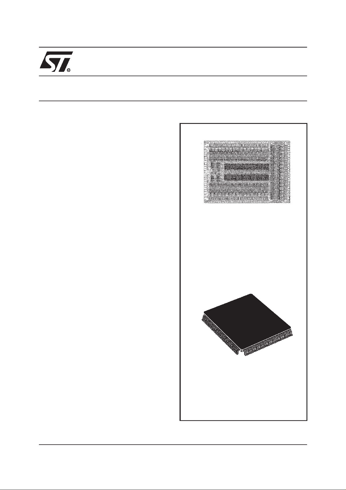
PLASMA DISPLAY PANEL DATA DRIVER
FEATURE
■ 96 OUTPUTS PLASMA DISPLAY DRIVER
■ 100 V ABSOLUTE MAXIMUM SUPPLY
■ 5 V SUPPLY FOR LOGIC
■ 60/50 mA SOURCE/SINK OUTPUT MOS
■ 60/50 mA SOURCE/SINK OUTPUT DIODE
■ 6 bit CASCADABLE DATA BUS (20 MHz)
■ BLANK, POLARITY CONTROL
■ BCD TECHNOLOGY
■ PACKAGING TQFP144 OR DICE
STV7610A
DESCRIPTION
The STV7610A is a BCD data driver for Plasma
Display Panel(PDP). Using a 6-bit wide cascadable data bus, it addresses 96 high current & high
voltage outputs. By serially connecting several
STV7610A, any horizontal pixel definition can be
performed. The 20 MHz shift clock gives an equivalent 120 MHz shift register. The STV7610A is
supplied with a separated90 V power output supply anda 5 V logic supply. All command inputs are
CMOS compatible.
ORDER CODE: STV7610A/WAF(1)
DIE
(1): Unsawn tested wafer
TQFP144 (20 x 20 x 1.4 mm)
(Thin Plastic Quad Flat Pack)
ORDER CODE: STV7610A
Version 4.2
June 2000 1/17
This ispreliminary information on a new product indevelopment orundergoing evaluation. Details are subject tochange without notice.
1
Page 2

STV7610A
PIN CONNECTIONS . . . . . . . . . . . . . . . . . . . . . . . . . . . . . . . . . . . . . . . . . . . . . . . . . . . ......... 3
PIN CONNECTIONS . . . . . . . . . . . . . . . . . . . . . . . . . . . . . . . . . . . . . . . . . . . . . . . . . . . ......... 4
PIN LIST . . ................................................................... 5
PAD COORDINATES (IN MM) . . . . ................................................ 6
BLOCK DIAGRAM . ............................................................ 9
CIRCUIT DESCRIPTION . . . . . . . . . ............................................... 10
NOTE 1 ABSOLUTE MAXIMUM RATINGS . . . . . . . .................................. 11
NOTE 4 THERMAL DATA . . . . . . . . ...............................................11
NOTE 4 ELECTRICAL CHARACTERISTICS ........................................12
NOTE 5 AC TIMINGS REQUIREMENTS . . . . . . . . . . ..................................13
NOTE 5 AC TIMINGS CHARACTERISTICS . . . . . . . . . . . . . . . . . . . . . . . . . . . . . . . . . ........ 13
FIGURE 2. INPUT/OUTPUT SCHEMATICS . . . . . . . . . . . . . . ........................... 15
FIGURE 6. PACKAGE MECHANICAL DATA . . . . . . . . . . . . . . . . . . . . . . . . . . . . . . . . ........ 16
2/16
2
Page 3
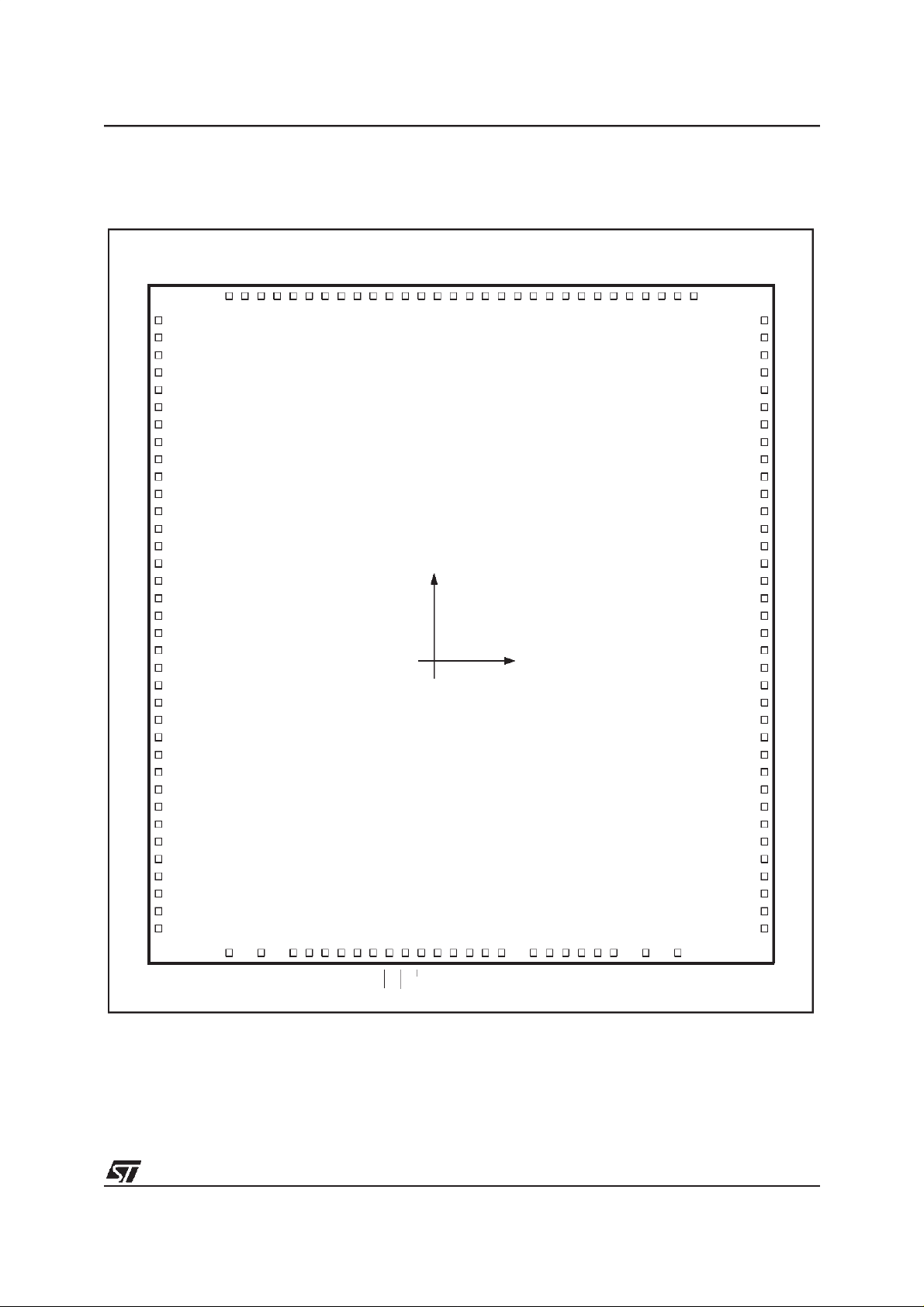
PIN CONNECTIONS
(DIE Pinout)
OUT63
OUT62
OUT61
OUT60
OUT59
OUT58
OUT57
OUT56
OUT55
OUT54
OUT53
OUT52
OUT51
OUT50
OUT49
OUT48
OUT47
OUT46
OUT45
OUT44
OUT43
OUT42
OUT41
OUT40
OUT39
OUT38
OUT37
OUT36
OUT35
STV7610A
OUT34
V
V
V
OUT64
OUT65
OUT66
OUT67
OUT68
OUT69
OUT70
OUT71
OUT72
OUT73
OUT74
OUT75
OUT76
OUT77
OUT78
OUT79
OUT80
OUT81
OUT82
OUT83
OUT84
OUT85
OUT86
OUT87
OUT88
OUT89
OUT90
OUT91
OUT92
OUT93
OUT94
OUT95
V
SSP
PP
PP
STV7610A
Bare Die
Y
(0,0)
X
SSP
V
PP
V
PP
OUT33
OUT32
OUT31
OUT30
OUT29
OUT28
OUT27
OUT26
OUT25
OUT24
OUT23
OUT22
OUT21
OUT20
OUT19
OUT18
OUT17
OUT16
OUT15
OUT14
OUT13
OUT12
OUT11
OUT10
OUT9
OUT8
OUT7
OUT6
OUT5
OUT4
OUT3
OUT2
OUT1OUT96
PP
SSP
V
V
B6B5B4B3B2
B1
BLK
POL
F/R
CC
V
SSSUB
CLK
SSLOG
V
V
A1A2A3A4A5
STB
PP
A6
SSP
V
V
3/17
3
Page 4
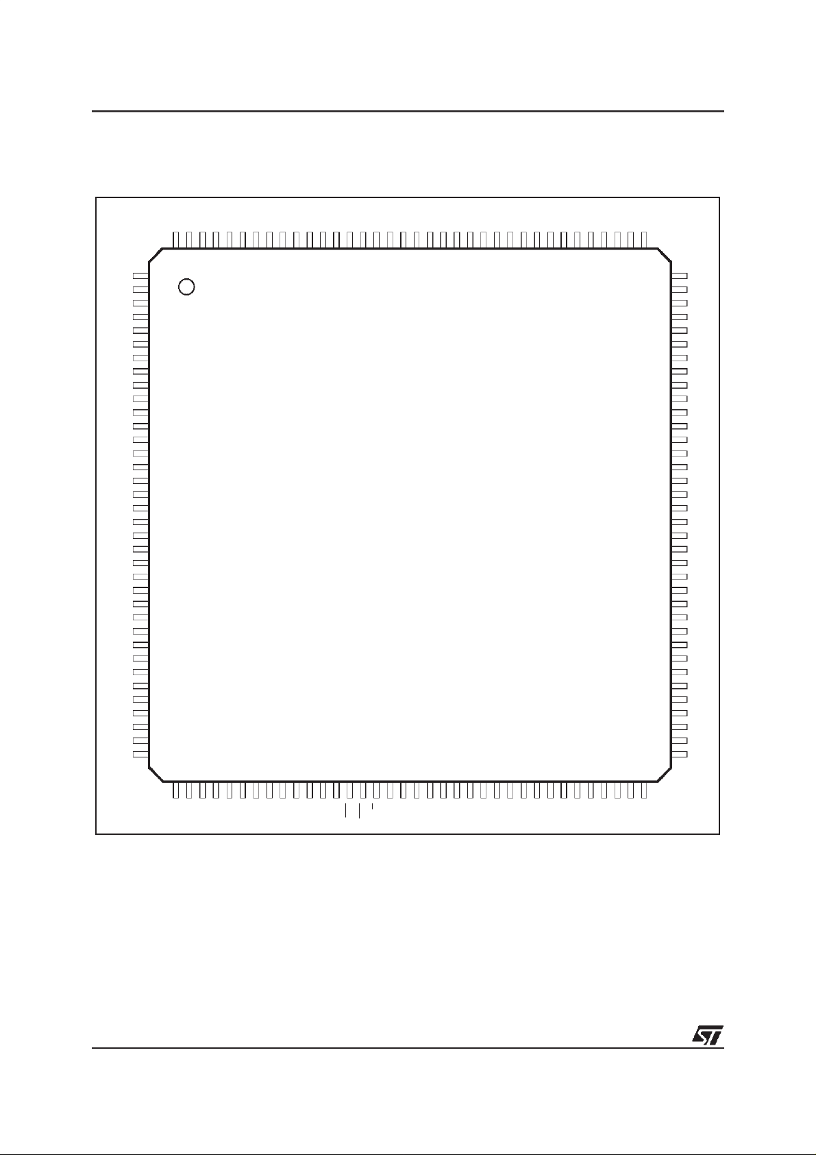
STV7610A
PIN CONNECTIONS
(TQFP Pinout)
V
V
OUT64
OUT65
OUT66
OUT67
OUT68
OUT69
OUT70
OUT71
OUT72
OUT73
OUT74
OUT75
OUT76
OUT77
OUT78
OUT79
OUT80
OUT81
OUT82
OUT83
OUT84
OUT85
OUT86
OUT87
OUT88
OUT89
OUT90
OUT91
OUT92
OUT93
OUT94
OUT95
SSP
OUT63
OUT62
OUT61
OUT60
OUT59
OUT58
OUT57
OUT56
OUT55
OUT54
OUT53
OUT52
OUT51
OUT50
OUT49
OUT48
OUT47
OUT46
OUT45
OUT44
OUT43
OUT42
OUT41
OUT40
OUT39
OUT38
OUT37
OUT36
OUT35
115
114
113
OUT34
112
V
NC
NC
144
143
142
141
140
139
138
137
136
135
134
133
132
131
130
129
128
127
126
125
124
123
122
121
120
119
118
117
1
PP
2
PP
3
4
5
6
7
8
9
10
11
12
13
14
15
16
17
18
19
20
21
22
23
24
25
26
27
28
29
30
31
32
33
34
35
36
3738394041424344454647484950515253545556575859606162636465666768697071
STV7610A
TQFP144
116
NCNCV
111
110
SSP
109
72
108
107
106
105
104
103
102
101
100
V
PP
V
PP
NCNC
OUT33
OUT32
OUT31
OUT30
OUT29
OUT28
99
OUT27
98
OUT26
97
OUT25
96
OUT24
95
OUT23
94
OUT22
93
OUT21
92
OUT20
91
OUT19
90
OUT18
89
OUT17
88
OUT16
87
OUT15
86
OUT14
85
OUT13
84
OUT12
83
OUT11
82
OUT10
81
OUT9
80
OUT8
79
OUT7
78
OUT6
77
OUT5
76
OUT4
75
OUT3
74
OUT2
73
OUT1OUT96
4/17
3
NCNCNC
SSP
V
VPPNC
NC
B6B5B4B3B2
B1
BLK
POL
F/R
CC
V
SSSUB
SSLOG
V
V
CLK
STB
NC
A1A2A3A4A5
PP
A6
NC
SSP
NC
NCNCNC
V
V
NC
Page 5
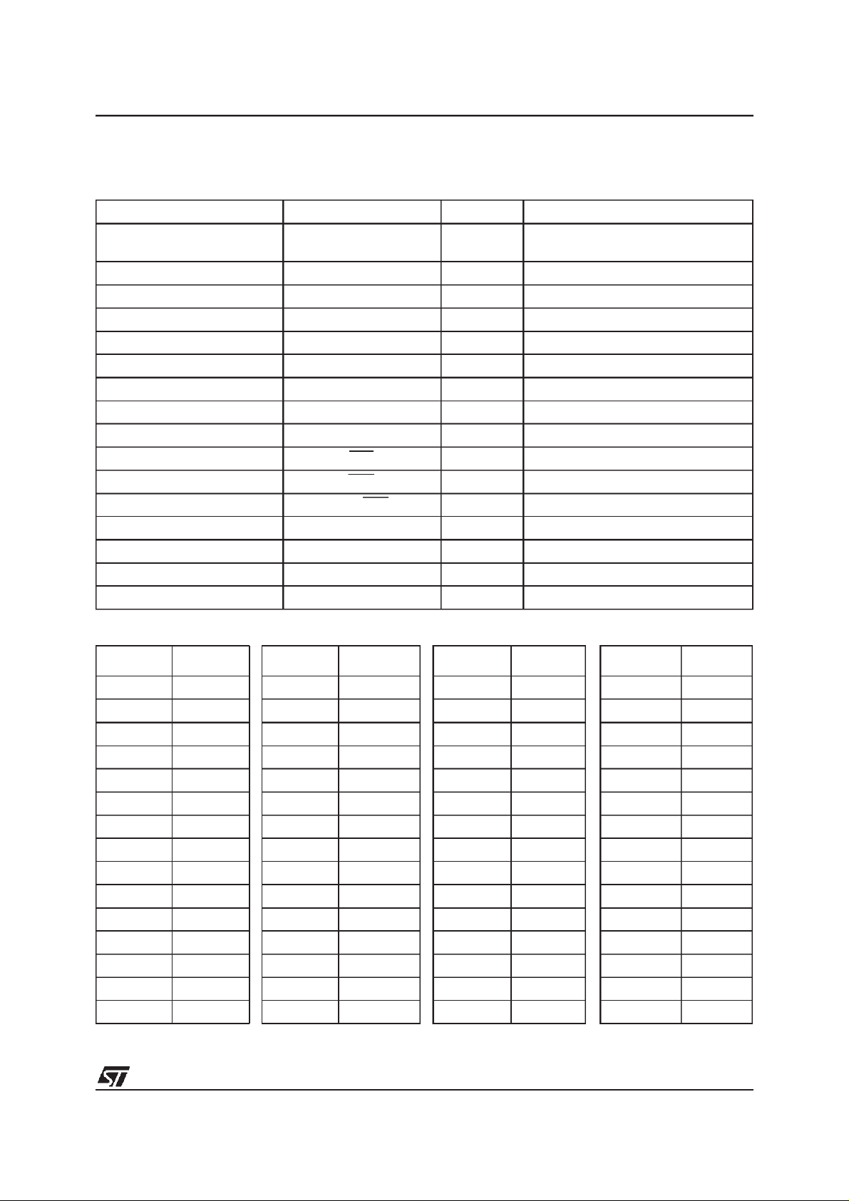
PIN LIST
(TQFP144)
Pin N° Symbol Type Description
3-37-38-39-41-43-48-65-67-69-
70-71-72-106-110-111-142-143
1-2-42-66-107-108 V
53 V
40-68-109-144 V
54 V
55 V
73 to 105 OUT 1 to OUT 33 Output Power Output
112 to 141 OUT 34 to OUT 63 Input Power Output
4 to 36 OUT 64 to OUT 96 Input Power Output
50 Input Blanking Input
51 Input Polarity Input
52 FOR/ Input Selection of Shift Direction
56 CLK Input Clock of data Shift Register
57 STB Input Latch of data to Outputs
59 to 64 A1 to A6 Input/Output Forward Shift Register Input
44 to 49 B6 to B1 Input/Output Forward Shift Register Output
-
PP
CC
SSP
SSLOG
SSSUB
BLK
POL
REV
STV7610A
NC
Supply High Voltage Supply of Power Outputs
Ground 5V Logic Supply
Ground Ground of Power Outputs
Ground Logic Ground
Output Substrate Ground
PIN LIST (Power outputs)
Output N° Pin N° Output N° Pin N° Output N° Pin N° Output N° Pin N°
1 73 25 97 49 127 73 13
2 74 26 98 50 128 74 14
3 75 27 99 51 129 75 15
4 76 28 100 52 130 76 16
5 77 29 101 53 131 77 17
6 78 30 102 54 132 78 18
7 79 31 103 55 133 79 19
8 80 32 104 56 134 80 20
9 81 33 105 57 135 81 21
10 82 34 112 58 136 82 22
11 83 35 113 59 137 83 23
12 84 36 114 60 138 84 24
13 85 37 115 61 139 85 25
14 86 38 116 62 140 86 26
15 87 39 117 63 141 87 27
5/17
3
Page 6
STV7610A
Output N° Pin N° Output N° Pin N° Output N° Pin N° Output N° Pin N°
16 88 40 118 64 4 88 28
17 89 41 119 65 5 89 29
18 90 42 120 66 6 90 30
19 91 43 121 67 7 91 31
20 92 44 122 68 8 92 32
21 93 45 123 69 9 93 33
22 94 46 124 70 10 94 34
23 95 47 125 71 11 95 35
24 96 48 126 72 12 96 36
PAD COORDINATES (in ΜM)
Pad positions from the middle of the top side
Name
OUT 48 74.0 3034.0 80.0 90.0
OUT 47 210.0 3034.0 80.0 90.0
OUT 46 346.0 3034.0 80.0 90.0
OUT 45 482.0 3034.0 80.0 90.0
OUT 44 618.0 3034.0 80.0 90.0
OUT 43 754.0 3034.0 80.0 90.0
OUT 42 890.0 3034.0 80.0 90.0
OUT 41 1026.0 3034.0 80.0 90.0
OUT 40 1162.0 3034.0 80.0 90.0
OUT 39 1298.0 3034.0 80.0 90.0
OUT 38 1434.0 3034.0 80.0 90.0
OUT 37 1570.0 3034.0 80.0 90.0
OUT 36 1706.0 3034.0 80.0 90.0
OUT 35 1842.0 3034.0 80.0 90.0
OUT 34 1993.0 3034.0 80.0 90.0
Center Size
XYXY
Pad positions along the right side
Name
V
SSP
V
PP
V
PP
Center Size
XYXY
2116.0 2795.0 90.0 80.0
2029.8 2496.5 90.0 90.0
2041.5 1843.0 90.0 80.0
Name
Center Size
XYXY
OUT 33 2117.0 1580.0 90.0 80.0
OUT 32 2117.0 1444.0 90.0 80.0
OUT 31 2117.0 1308.0 90.0 80.0
OUT 30 2117.0 1172.0 90.0 80.0
OUT 29 2117.0 1036.0 90.0 80.0
OUT 28 2117.0 900.0 90.0 80.0
OUT 27 2117.0 764.0 90.0 80.0
OUT 26 2117.0 628.0 90.0 80.0
OUT 25 2117.0 492.0 90.0 80.0
OUT 24 2117.0 356.0 90.0 80.0
OUT 23 2117.0 220.0 90.0 80.0
OUT 22 2117.0 84.0 90.0 80.0
OUT 21 2117.0 2117.0 90.0 80.0
OUT 20 2117.0 2117.0 90.0 80.0
OUT 19 2117.0 -324.0 90.0 80.0
OUT 18 2117.0 -460.0 90.0 80.0
OUT 17 2117.0 -596.0 90.0 80.0
OUT 16 2117.0 -732.0 90.0 80.0
OUT 15 2117.0 -868.0 90.0 80.0
OUT 14 2117.0 -1004.0 90.0 80.0
OUT 13 2117.0 -1140.0 90.0 80.0
OUT 12 2117.0 -1276.0 90.0 80.0
OUT 11 2117.0 -1412.0 90.0 80.0
6/17
3
Page 7

STV7610A
Name
XYXY
OUT 10 2117.0 -1548.0 90.0 80.0
OUT 9 2117.0 -1684.0 90.0 80.0
OUT 8 2117.0 -1820.0 90.0 80.0
OUT 7 2117.0 -1956.0 90.0 80.0
OUT 6 2117.0 -2092.0 90.0 80.0
OUT 5 2117.0 -2228.0 90.0 80.0
OUT 4 2117.0 -2364.0 90.0 80.0
OUT 3 2117.0 -2500.0 90.0 80.0
OUT 2 2117.0 -2636.0 90.0 80.0
OUT 1 2117.0 -2832.0 90.0 80.0
Pad positions along the bottom side
Center Size
Name
V
SSP
V
PP
A6 1499.0 -3034.0 80.0 90.0
A5 1349.0 -3034.0 80.0 90.0
A4 1199.0 -3034.0 80.0 90.0
Center Size
XYXY
1904.0 -3034.0 80.0 90.0
1698.0 -3034.0 80.0 90.0
Name
XYXY
A3 1049.0 -3034.0 80.0 90.0
A2 899.0 -3034.0 80.0 90.0
A1 749.0 -3034.0 80.0 90.0
STB 449.0 -3034.0 80.0 90.0
CLK 299.0 -3034.0 80.0 90.0
GNDsub 156.5 -3034.0 80.0 90.0
GND 3.0 -3034.0 80.0 90.0
Center Size
V
CC
-158.0 -3034.0 80.0 90.0
F/R -299.0 -3034.0 80.0 90.0
POL -449.0 -3034.0 80.0 90.0
BLK -599.0 -3034.0 80.0 90.0
B1 -749.0 -3034.0 80.0 90.0
B2 -899.0 -3034.0 80.0 90.0
B3 -1049.0 -3034.0 80.0 90.0
B4 -1199.0 -3034.0 80.0 90.0
B5 -1349.0 -3034.0 80.0 90.0
B6 -1499.0 -3034.0 80.0 90.0
-1698.0 -3034.0 80.0 90.0
PP
-1904.0 -3034.0 80.0 90.0
V
V
SSP
7/17
3
Page 8

STV7610A
Pad Positions along the left side
Name
OUT 96 -2117.0 -2832.0 90.0 80.0
OUT 95 -2117.0 -2636.0 90.0 80.0
OUT 94 -2117.0 -2500.0 90.0 80.0
OUT 93 -2117.0 -2364.0 90.0 80.0
OUT 92 -2117.0 -2228.0 90.0 80.0
OUT 91 -2117.0 -2092.0 90.0 80.0
OUT 90 -2117.0 -1956.0 90.0 80.0
OUT 89 -2117.0 -1820.0 90.0 80.0
OUT 88 -2117.0 -1684.0 90.0 80.0
OUT 87 -2117.0 -1548.0 90.0 80.0
OUT 86 -2117.0 -1412.0 90.0 80.0
OUT 85 -2117.0 -1276.0 90.0 80.0
OUT 84 -2117.0 -1140.0 90.0 80.0
OUT 83 -2117.0 -1004.0 90.0 80.0
OUT 82 -2117.0 -868.0 90.0 80.0
OUT 81 -2117.0 -732.0 90.0 80.0
OUT 80 -2117.0 -596.0 90.0 80.0
OUT 79 -2117.0 -460.0 90.0 80.0
OUT 78 -2117.0 -324.0 90.0 80.0
OUT 77 -2117.0 -188.0 90.0 80.0
OUT 76 -2117.0 -52.0 90.0 80.0
OUT 75 -2117.0 84.0 90.0 80.0
OUT 74 -2117.0 220.0 90.0 80.0
OUT 73 -2117.0 356.0 90.0 80.0
OUT 72 -2117.0 492.0 90.0 80.0
OUT 71 -2117.0 628.0 90.0 80.0
OUT 70 -2117.0 764.0 90.0 80.0
Center Size
XYXY
Name
OUT 69 -2117.0 900.0 90.0 80.0
OUT 68 -2117.0 1036.0 90.0 80.0
OUT 67 -2117.0 1172.0 90.0 80.0
OUT 66 -2117.0 1308.0 90.0 80.0
OUT 65 -2117.0 1444.0 90.0 80.0
OUT 64 -2117.0 1580.0 90.0 80.0
V
PP
V
PP
V
SSP
Center Size
XYXY
-2041.5 1843.0 90.0 80.0
-2029.8 2496.5 90.0 80.0
2116.0 2795.5 90.0 80.0
Pad Positions along the top side
Name
OUT 63 -1980.0 3034.0 80.0 90.0
OUT 62 -1830.0 3034.0 80.0 90.0
OUT 61 -1694.0 3034.0 80.0 90.0
OUT 60 -1558.0 3034.0 80.0 90.0
OUT 59 -1422.0 3034.0 80.0 90.0
OUT 58 -1286.0 3034.0 80.0 90.0
OUT 57 -1150.0 3034.0 80.0 90.0
OUT 56 -1014.0 3034.0 80.0 90.0
OUT 55 -878.0 3034.0 80.0 90.0
OUT 54 -742.0 3034.0 80.0 90.0
OUT 53 -606.0 3034.0 80.0 90.0
OUT 52 -470.0 3034.0 80.0 90.0
OUT 51 -334.0 3034.0 80.0 90.0
OUT 50 -198.0 3034.0 80.0 90.0
OUT 49 -62.0 3034.0 80.0 90.0
Center Size
XYXY
8/17
3
Page 9

BLOCK DIAGRAM
56
59 49
60 48
A2
61 47
A3
62 46
A4
63 45
A5
16-BIT SHIFT REGISTER
P1 P91
16-BIT SHIFT REGISTER
P2 P92
16-BIT SHIFT REGISTER
P3 P93
16-BIT SHIFT REGISTER
P4 P94
16-BIT SHIFT REGISTER
P5 P95
STV7610A
FOR/REVCLK
52
V
CC
B1A1
B2
B3
B4
B5
64 44
A6
57
STB
V
CC
50
POL
V
CC
51
BLK
16-BIT SHIFT REGISTER
P6 P96
P96P95P6P1
LATCH
Q1 Q96
Q2 Q95
LOGIC
73 36
STV7610A
OUT1 OUT96
B6
54
V
SSLOG
55
V
SSSUB
53
V
CC
V
SSP
Pins40-68-109-144
V
PP
Pins1-2-42-66-107-108
9/17
3
Page 10

STV7610A
CIRCUIT DESCRIPTION
The STV7610A contains all the logic and the power circuits necessary to drive the columns of a
Plasma Display Panel (P. D. P.). The binary value
of each pixel of the displayed line is loaded into the
shift register. Data are input in a 6-bit wide data
bus to A1 - A6 input (case of forward shift mode).
Data are shifted at each low to high transition of
the CLKshift clock. After 16 shifts thefirst data are
available on B1 - B6 outputs. These B1 - B6 outputs can be used to cascade several drivers to
perform any horizontal resolution. The forward/
reverse REV
direction of the shift register, A1 - A6 and B1 - B6
data bus input/output status is set according to the
selected direction. FOR/ = H, A is an input
and B is an output.
(FOR/ ) input is used to select the
REV
V
SSSUB
and V
SSLOG
must be connected as close
as possible to the logical reference ground of the
application.
Shift Register Truth Table
Input Input/Outp ut
FOR/ CLK A B Output Q
REV
H Rise IN OUT Forward shift
H H or L IN OUT Steady
L Rise OUT IN Reverse shift
L H or L OUT IN Steady
Shift Register
Function
Serial inputs, CLK, STB inputs are Smith trigger inputs. If not used in the application, Blanking
( ), Polarity ( are internaly pulled to level
BLK
POL
”H”. The maximum frequency of the shift clock is
20 MHz. This leads to an equivalent 120 MHz serial shiftregister.
On low level of STB, data is transferred from shift
register to the latch stage. Data will not be refreshed as long as STB is kept high.
Blanking input ( ) forces the power outputs to
BLK
low level when pulled low. All the power outputs
are set at high level when the Polarity command
POL
( ) is pulled low and the Blanking ( ) input
BLK
is at high level.
Power Output Truth Table
Driver
Qn STB
X X L X L Output low
X X H L H Output high
X H H H Qn Data latched
L L H H L Data copied
H L H H H Data copied
Note 1 Qn+1 = A1, Qn + 2 = A2, Qn + 3 = A3, Qn + 4 =
A4, Qn +5= A5, Qn + 6= A6, n= [0,6,12,18,...,90]
BLK
POL
Output
Comments
10/17
3
Page 11

STV7610A
ABSOLUTE MAXIMUM RATINGS
Symbol Parameter Value Unit
V
CC
OUTi
V
IN
V
OUT
I
POUT
I
DOUT
T
j
T
oper
T
stg
Note 2 Through one power output (all power outputs).
Note 3 Through one power output for all power outputs (see Test Diagram) with Junction temperature lower or equal than
max.
T
j
Note 4 These parameters are measured during ST’s internal qualification which includes temperature characterisation
on standard batches and on corners batches of the process. These parameters are not tested on the parts.
Logic Supply Range (Pin 53) -0.3, +7 V
Output Pins (4 to 36, 73 to 105, 112 to 141) -0.3, +100 V
Logic Input Voltage (Pins 50, 51, 52, 56, 57, 59 to 64)
Logic Output Voltage (Pin 44 to 49)
-0.3, +V
-0.3, +V
CC
CC
+0.3
+0.3
V
V
Driver Output Current ( Note 2) ( Note 4) -60/ +50 mA
Diode Output Current ( Note 3) ( Note 4) -50/ +60 mA
Junction Temperature +150 °C
Operating Temperature -20, +85 °C
Storage Temperature -50, +150 °C
THERMAL DATA
Symbol Parameter Value Unit
R
th(j-a)
Junction-ambient Thermal Resistance Typ. 41 °C/W
11/17
3
Page 12

STV7610A
ELECTRICAL CHARACTERISTICS
(VCC=5V,VPP=90V,V
otherwise specified)
Symbol Parameter Test Conditions Min. Typ. Max. Unit
SUPPLY
V
CC
I
CCH
I
CCL
V
PP
I
PPH
OUTPUT (V
OUT 1- OUT 96
V
POUTH
V
POUTL
V
DOUTH
V
DOUTL
A1-A6, B1-B6
V
OH
V
OL
INPUT
CLK, FOR/ , STB, , , A1-A6, B1-B6
V
IH
V
IL
I
IH
I
IL
Logic Supply Voltage 4.5 5 5.5 V
Logic Supply Current (all inputs high) - - 100 µA
Logic Dynamic Supply Current f
Power Output Supply Voltage 15 - 90 V
Power Output Supply Current
(steady outputs)
= 15 V to 90 V)
PP
Power Output Voltage Drop
(High Level) (versus V
Power Output Voltage Drop
(Low Level)
Output Diode Voltage (High Level) I
Output Diode Low Level I
Logic Output (High Level) IOH= -1 mA 4 4.2 - V
Logic Output (Low Level) IOL= +1 mA - 0.12 0.4 V
REV POL BLK
Input Voltage (High Level)
Input Voltage (Low Level) - High Level Input Current VIH=V
Low Level Input Current
CLK, A1-A6, B1-B6, STB,
FOR/ , ,
REV BLK P OL
SSP
=0V,V
)
PP
SSLOG
=0V,V
SSSUB
= 20 MHz - 26 - mA
CLK
=0V,T
amb
=25°C, f
= 20 MHz, unless
CLK
--100µA
I
= - 30 mA
POUTH
= - 45mA
I
POUTH
=+30mA - 1.6 4 V
I
POUTL
= +45 mA ( Note 5) - 1.05 4 V
DOUTH
= - 30mA ( Note 5) - -0.95 -4 V
DOUTL
CC
-
-
0.8 V
4.0
4.5
--V
CC
--10µA
VIL=0V
-
-
-
-
6.0
6.5
0.2V
-10
-40
CC
V
V
V
µA
µA
Note 5 See test diagram page 14.
12/17
3
Page 13

STV7610A
AC TIMINGS REQUIREMENTS
(VCC=4.5 Vto 5.5 V,T
Symbol Parameter Min. Typ. Max. Unit
= -20 to +85°C, input signalsmax leading edge & trailing edge (tR,tF) = 10 ns)
amb
t
WHCLK
t
WLCLK
t
SDAT
t
HDAT
t
SFR
t
DSTB
t
SSTB
t
STB
t
BLK
t
POL
Duration of clock (CLK) pulse at high level 15 - - ns
Duration of clock (CLK) pulse at low level 15 - - ns
Set-up Time of data input before clock (low to high) transition 10 - - ns
Hold Time of data input after clock (low to high) transition 10 - - ns
Forward/ (FOR/ ) Set-up Time before clock (low to
high) transition
Minimum Delay to latch after clock (low to high) transition 10 - - ns
Minimum Delay to latch before clock (low to high) transition 10 - - ns
Latch Low Level Pulse Duration 20 - - ns
Blanking Pulse Duration 500 - - ns
Polarity Pulse Duration 500 - - ns
reverse REV
STB()
STB()
STB()
BLK()
POL()
100
AC TIMINGS CHARACTERISTICS
(VCC=5V,VPP=90V,V
(V
IL(Max.)
Symbol Parameter Min. Typ. Max. Unit
t
t
RDAT
t
FDAT
t
PHL1
t
PLH1
t
PHL2
t
PLH2
t
PHL3
t
PLH3
t
PHL4
t
PLH4
CLK
= 0.2 Vcc, V
IH(Min.)
Data clock Period 50 - - ns
Logical Data Output Rise Time (CL=10pF) - 12 20 ns
Logical Data Output Fall Time(CL=10pF) - 11 20 ns
Delay of logic data output (high to low transition) after clock (CLK) transition
Delay of logic data output (low to high transition) after clock (CLK) transition
Delay of power output change (high to low transition) after clock (CLK) transition
Delay of power output change (low to high transition) after clock (CLK) transition
Delay of power output change (high to low transition) after Latch (STB) transition
Delay of power output change (low to high transition) after Latch (STB) transition
Delay of power output change (high to low transition) to Blank or Polarity
( , ) transition
BLK POL
Delay of power output change (low to high transition) to Blank or Polarity
( , ) transition
BLK POL
SPP
=0V,V
SSLOG
=0V,V
SSSUB
=0V,T
amb
=25°C)
= 0.8 VCC,VOH= 4.0V,VOL= 0.4 V,unless otherwise specified)
--30305050ns
--13580180
180nsns
--11570165
165nsns
--10055160
160nsns
ns
t
ROUT
t
FOUT
Power Output Rise Time ( Note 6) - 50 150 ns
Power Output Fall Time ( Note 6) - 80 200 ns
Note 6 One outputamong 96, loading capacitor CL= 50pF, other outputs at low level.
13/17
3
Page 14

STV7610A
Figure 1. : AC Characteristics Waveform
t
WHCLK
t
CLK
t
WLCLK
“1”
CLK
A INPUT
B OUTPUT
STB
50%
F/R
OUTn
(POL=#0#)
BLK
OUTn
50%
t
STB
t
PHL3
t
PLH3
50%
10%
50%
t
SDAT
50%
50%
t
FDAT
90%
90%
10%
t
RDAT
t
DSTB
t
SSTB
t
SFR
90%
10%
t
BLK
50% 50%
t
PHL4
90%
t
PHL2
t
PLH2
90%
10%
t
HDAT
t
PHL1
t
PLH1
t
PLH4
90%
“0”
“1”
50%
“0”
“1”
“0”
“1”
“0”
“1”
“0”
“1”
“0”
“1”
“0”
“1”
14/17
3
t
F OUT
10%
10%
t
R OUT
“0”
Page 15

Figure 2. : Test Configuration
STV7610A
V
V
PP=
SSP
V
DOUTH
V
SSP
Output sinking current as positive value, sourcing current as negative value
INPUT/OUTPUT SCHEMATICS
Figure 3. : , , F/ Input
POL,BLK, F/R
Pins 51, 50, 52
PO L BLK R
V
CC
I
DOUTH
V
CC
V
PP=VSSP
V
DOUTL
V
SSP
Figure 5. : A1 to A6, B1 to B6
V
CC
A1 to A6,
B1 to B6
Pins 59 to 64,
49 to 44
V
CC
I
DOUTL
V
CC
GNDLOG
GNDSUB
Figure 4. : CLK, STB Input
V
CC
CLK, STB
Pins 56, 57
GNDSUB
GNDLOG
V
CC
GNDLOG
GNDSUB
Figure 6. : Power Output
V
PP
V
SSP
OUT1 to OUT 96
Pins 73 to 105,
112 to 141, 4 to 36
15/17
3
Page 16

STV7610A
PACKAGE MECHANICAL DATA
144 PINS - THIN PLASTIC QUAD FLAT PACK (TQFP)
144 109
1
36 73
e
108
E3
E
E1
0,076 mm
0.03 inch
SEATING PLANE
A
A2
A1
B
37 72
D3
D1
D
L1
L
0,25 mm
.010 inch
GAGE PLANE
K
c
Millimeters Inches
Dimensions
Min. Typ. Max. Min. Typ. Max.
A 1.60 0.063
A1 0.05 0.15 0.002 0.006
A2 1.35 1.40 1.45 0.053 0.055 0.057
B 0.17 0.22 0.27 0.0067 0.0087 0.011
C 0.09 0.20 0.0035 0.008
D 22.00 0.866
D1 20.00 0.787
D3 17.50 0.689
e 0.50 0.020
E 22.00 0.866
E1 20.00 0.787
E3 17.50 0.689
L 0.45 0.60 0.75 0.018 0.024 0.030
L1 1.00 0.039
K0°(Min.), 7° (Max.)
16/17
Page 17

STV7610A
Information furnished isbelieved to be accurate and reliable. However, STMicroelectronics assumes no responsibility for the consequences of use of such information nor for any infringement of patents or other rights of
third parties which may result from its use. No license is granted by implication or otherwise under any patent
or patent rights of STMicroelectronics. Specifications mentioned in this publication are subject to change without notice. This publication supersedes and replaces all information previously supplied. STMicroelectronics
products are not authorized for use as critical components in life support devices or systems without express
written approval of STMicroelectronics.
The ST logo is a trademark of STMicroelectronics.
2000 STMicroelectronics - All Rights Reserved
2
Purchase of I
Rightsto use these componentsin a I
Australia - Brazil - China -Finland - France - Germany - Italy - Japan - Korea - Malaysia - Malta - Mexico - Morocco - The
Netherlands - Singapore - Spain - Sweden - Switzerland - Taiwan - Thailand - United Kingdom - U.S.A.
C Components ofSTMicroelectronics, conveys a license under the Philips I2C Patent.
2
C system, is granted provided that the system conforms to the I2C Stan-
dard Specifications as defined by Philips.
STMicroelectronics GROUP OF COMPANIES
http://www.st.com
17/17
4
 Loading...