

Page 1
STPC® ELITE
X86 Core General Pur pose PC Compat i ble System - on - Chip
Release 1.3 - January 29, 2002 1/87
This is preliminary information on a new product now in development or undergoing evaluation. Details are subject to change without notice.
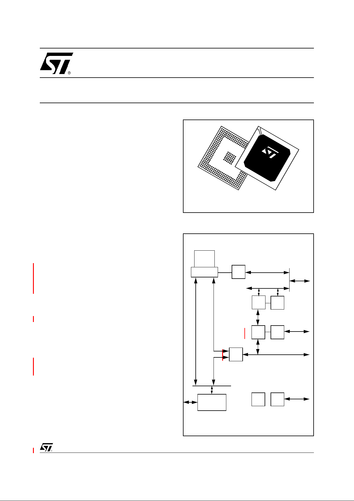
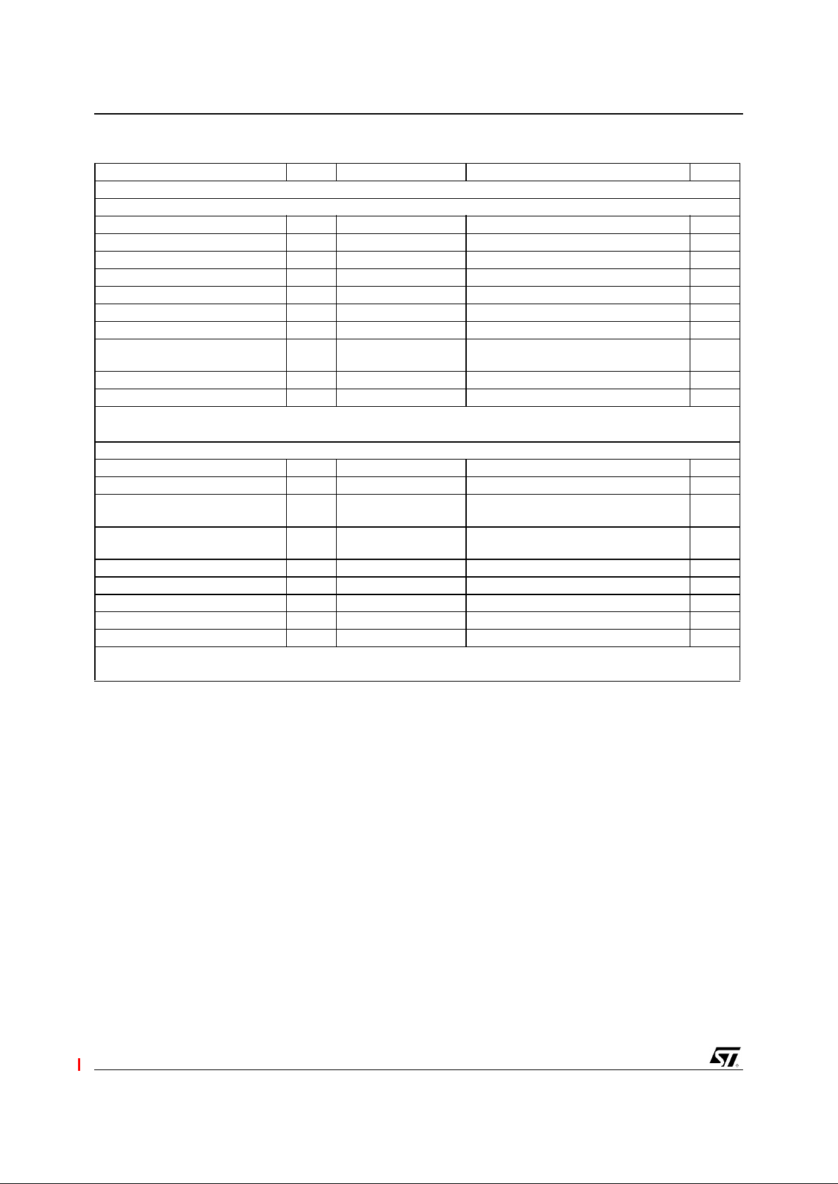
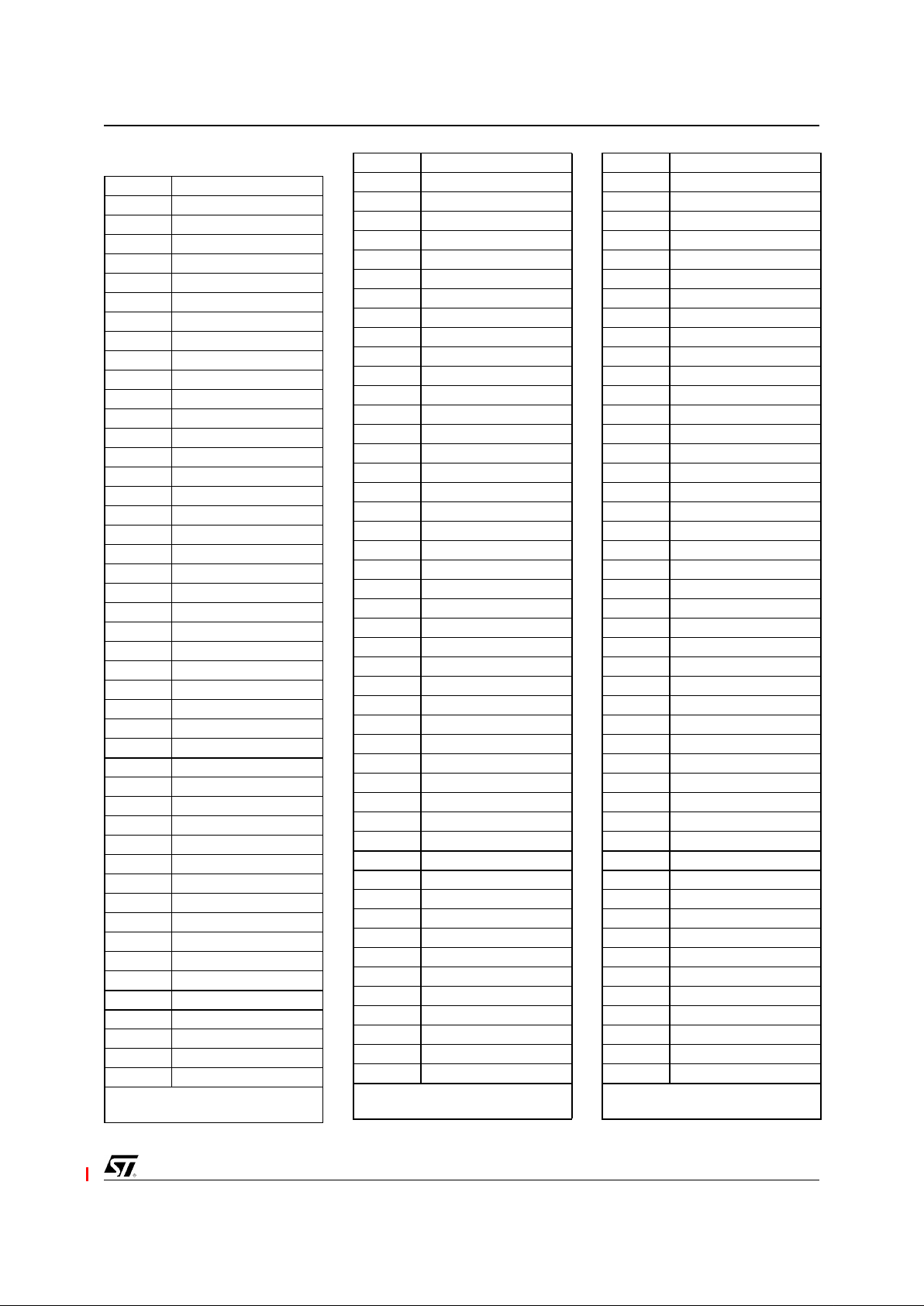
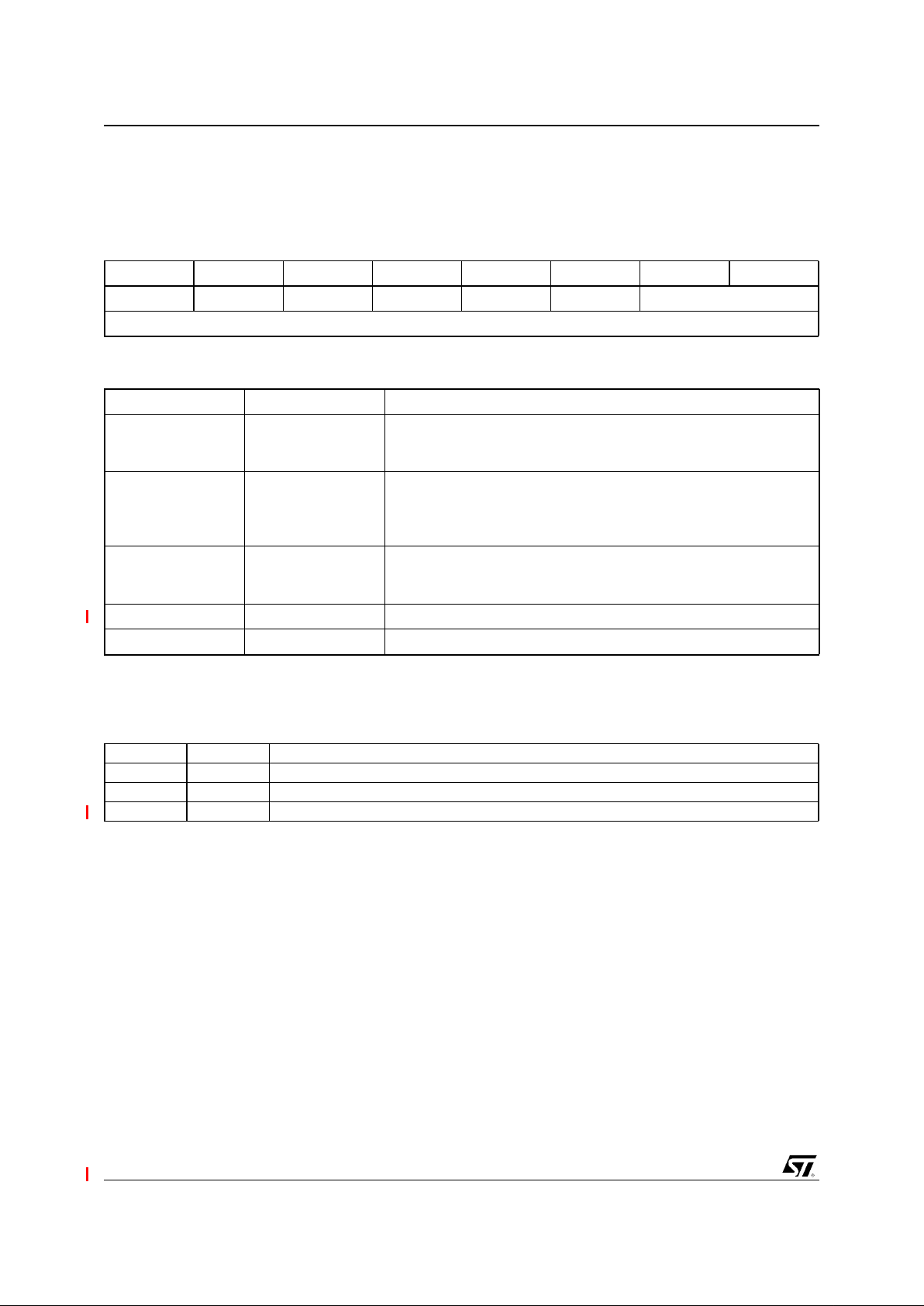
Logic Diagram
■
POWERFUL X86 PROCESSOR
■
64-BIT SDRAM CONTROLLER AT 100MHz
■
INTEGRATED PCI NORTH / SOUTH
BRIDGE CONTROLLER
■
ISA MASTER / SLAVE / DMA
■
16-BIT LOCAL BUS INTERFACE FOR LOW
COST AND EMBEDDED APPLICATIONS
■
EIDE CONTROLLER
■
INTEGRATED PERIPHERAL CONTROLLER
- DMA CONTROLLER
- INTERRUPT CONTROLLER
- TIMER / COUNTERS
■
POWER MANAGEMENT UNIT
■
I²C INTERFACE
■
16 ENHANCED GENERAL PURPOSE I/Os.
■
JTAG IEEE1149.1
■
PROGRAMMABLE OUTPUT CLOCK UP TO
135MHz
■
COMMERCIAL AND INDUSTRIAL TEMPERATURE RANGES
DESCRIPTION
The STPC Elite integrates a fully static x86
processor up to 133 MHz, fully compatible with
standard x86 processors, and combines it with
powerful chipset to provide a general purpose P C
compatible subsystem on a single device. The
device is packaged in a 388 Ball Grid Array
(PBGA).
The STPC Elite has a low voltage operation with
V
CORE
= 2.5V and has 5V tolerant I/Os (3.3V
output levels).
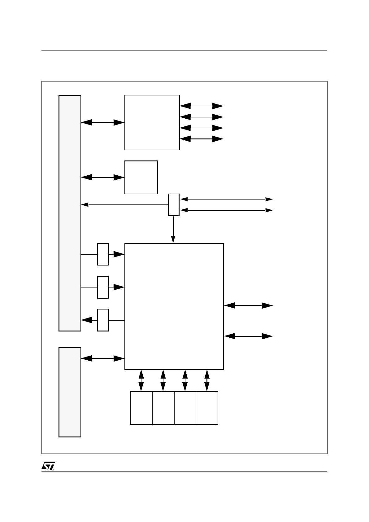
PBGA388
S
T
P
C
E
L
I
T
E
x86
Core
Host I/F
SDRAM
CONTROL
PCI
I/F
PCI
ISA
I/F
EIDE
ctrl
PCI
I/F
ISA BUS
EIDE
L.B.
I/F
LOCAL BUS
IPC
JTAGPMU
Page 2

2/87
Release 1.3 - Januar
y
29, 2002
This is preliminary information on a new product now in development or undergoing evaluation. Details are subject to change without notice.
■
X86 Processor core
■
Fully static 32-bit 5-stage pipeline, x86
processor fully PC compatib l e .
■
Can access up to 4GB of external memory .
■
8KByte unified instruction and data cache
with write back and write through capability.
■
Parallel processing integral floating point unit,
with automatic power down.
■
Clock core speeds up to of 100 MHz in x1
clock mode and 133MHz in x2 mode.
■
Fully static design for dynamic clock control.
■
Low power and system management modes.
■
SDRAM Controller
■
64-bit data bus.
■
Up to 100MHz SDRAM clock speed.
■
Supports up to 128 MB system memory .
■
Support s 16-, 64- and 128-Mbit memorie s.
■
Supports up to 4 memory banks.
■
Supports buffered, non buffered, registered
DIMMs
■
4-line write buffers f or CPU to DRAM and PCI
to DRAM cycles.
■
4-line read prefetch buffers for PCI masters.
■
Programmable latency
■
Programmable timing for DRAM parameters.
■
Support s -8, -10, -12, -13, -15 memory par t s
■
Supports memory hole between 1MB and
8MB for PCI/ISA busses.
■
PCI Controller
■
Compliant with PCI 2.1 specification.
■
Integrated PCI arbitration interface. Up to 3
masters can connect directly. External logic
allows for greater than 3 masters.
■
Translation of PCI cycles to ISA bus.
■
Tr a n slation of ISA master ini ti a te d cycle to
PCI.
■
Support for burst read/write from PCI master.
■
0.25X, 0.33X and 0.5X Host clock PCI clock.
■
ISA master/slave
■
Generates the ISA clock from either
14.318 MH z o s c illator clock or PCI c lo ck
■
Support s programmable extra wait state for
ISA cycles
■
Supports I/O recovery time for back to back
I/O cycles.
■
Fast Gate A20 and Fast reset.
■
Support s the single ROM that C, D, or E.
blocks shares with F block BIOS ROM.
■
Support s flash ROM.
■
Support s ISA hidden re fresh.
■
Buffered DMA & ISA master cycl es t o reduce
bandwidth utilization of the PCI and Host
bus. NSP compliant.
■
16-bit I/O decoding.
■
Local Bus interface
■
Multiplexed with ISA/DMA/Timer functions.
■
High speed, low latency bus.
■
Support s 32-bit Flash burst.
■
16-bit data bus with word steering capability.
■
Separate memory and I/O addres s spac es.
■
Programmable timing (Host clock granularity)
■
Supports 2 cachable banks of 16MB flash
devices with boot block shadowed to
0x000F0000.
■
2 Programmable Flash/EPROM Chip Select.
■
4 Programmable I/O Chip Select.
■
2-level hardware ke y protection for Flash boot
block protection.
■
24 bit address bus.
■
EIDE Controller
■
Compatible with EIDE (ATA-2).
■
Backward compatibilit y wit h ID E (ATA-1).
■
Supports up to 4 IDE devices
■
Support s PIO and Bu s Master IDE
■
Concurrent channel operation (PIO & DMA
modes) - 4 x 32-Bit Buffer FIFO per channel
■
Support for 11.1/16.6 MB/s, I/O Channel
Ready PIO data transfers.
■
Bus Master with scatter/gather capability.
■
Multi-word DMA suppor t for fast IDE drives.
■
Individual drive timing for all four IDE devices.
■
Support s both legacy & native IDE modes.
■
Supports hard drives larger than 528MB.
■
Support for CD-ROM and tape peripherals.
■
Integrated Peripheral Controller
■
2X8237/AT compatible 7-channel DMA
controller.
■
2X8259/AT compatible interrupt Controller.
16 interrupt inputs - ISA and PCI.
■
Three 8254 compatible Timer/Counters.
■
Co-processor error support logic.
■
Support s external RTC.
■
Power Management
■
Four power saving modes: On, Doze,
Standby, Suspend.
Page 3

Release 1.3 - January 29, 2002 3/87
This is preliminary information on a new product now in development or undergoing evaluation. Details are subject to change without notice.
■
Programmable system activity detector
■
Supports SMM.
■
Supports STOPCLK.
■
Support s IO trap & restart .
■
Independent peripheral time-out timer to
monitor hard disk, serial & parallel ports.
■
Supports RTC, interrupts and DMAs wake-up
■
GPIOs
■
16 Enhanced General Purpose IO.
■
JTAG Function
■
Programmable GP-Clock
■
This clock is programmable to frequencies up
to 135 MHz.
Page 4

4/87
Release 1.3 - Januar
y
29, 2002
This is preliminary information on a new product now in development or undergoing evaluation. Details are subject to change without notice.
Page 5
GENERAL DESCRIPTION
Release 1.3 - January 29, 2002 5/87
This is preliminary information on a new product now in development or undergoing evaluation. Details are subject to change without notice.
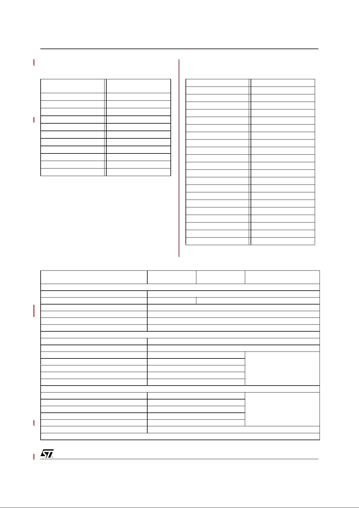
1. GENERAL DESCRIPTION
At the heart of the STPC Elite is an advanced
processor block that includes a powerful x86
processor core along with a 64-bit SDRAM
controller, a high speed PCI local-bus controller
and Industry standard PC chip set functions
(Interrupt controller, DMA Controller, Interval timer
and ISA bus) and EIDE controller.
The processor bus runs at the speed of the
processor (x1 mode) or half the speed (x2 mode).
The STMicroelectronics x86 processor core is
embedded with standard and app lication specific
peripheral modules on the sa me silicon die. The
core has all the functionality of the ST standard
x86 processor products, including the low power
System Management Mode (SMM).
System Management Mode (SMM) provides an
additional interrupt and address space that can be
used for system power management or software
transparent emulation of peripherals. While
running in isolated SMM address space, the SMM
interrupt routine can execute without interfering
with the operating system or application
programs.
The ‘standard’ PC chipset functions (DMA,
interrupt controller, timers, power management
logic) are integrated with the x86 processor core.
The PCI bus is the ma in data comm unication link
to the STPC Elite chip. The STPC Elite translates
appropriate host bus I/O an d M em ory cycles onto
the PCI bus. It also supports generation of
Configuration cycles on the PCI bus. The STPC
Elite, as a PCI bus agent (host bridge class), f ully
complies with PCI specificat ion 2.1. The chip-set
also implements the PCI mandatory header
registers in Type 0 PCI configuration space for
easy porting of PCI aware system BIOS. The
device contains a PCI arbitration function for three
external PC I dev i ces.
The STPC Elite integrates an ISA bus controller.
Peripheral modules such as parallel and serial
communications ports, keyboard controllers and
additional ISA devices can be accessed by the
STPC Elite chip set through this bus.
An industry standard EIDE (ATA 2) controller is
built in to the STPC Elite and connected internally
via the PCI bus.
1.1. MEMORY CONTROLLER
The STPC handles the mem ory data (DATA) bus
directly, controlling from 8 to 128 MBytes. The
SDRAM controller supports accesses to the
Memory Banks to/from the CPU (via the host).
Parity is not supported.
The SDRAM controller only supports 64 bit wide
Memory Banks.
Four Memory Banks (if DIMMS are used; Single
sided or two double-sided DIMMs) are s upported
in the following configurations (see Table 1-1)
The SDRAM Controller supports buffered or
unbuffered SDRAM but not EDO o r FPM modes.
SDRAMs must support Full Page Mode Type
access.
The STPC Memory Controller provides various
programmable SDRAM parameters to allow the
SDRAM interface to be optimized for different
processor bus speeds SDRAM speed grades and
CAS Latency.
1.2. POWER MANAGEMENT
The STPC Elite core is compliant with the
Advanced Power Management (APM)
specification to provide a standard method by
which the BIOS can control the power used by
personal computers. The Power Management
Unit (PMU) module controls the power
consumption, providing a comprehensive set of
features that controls the power usage and
supports compliance with the United States
Environmental Protection Agency's Energy Star
Computer Program. The PMU provides the
following hardware structures to assist the
software in managing the system power
consumption:
- System Activity Detection.
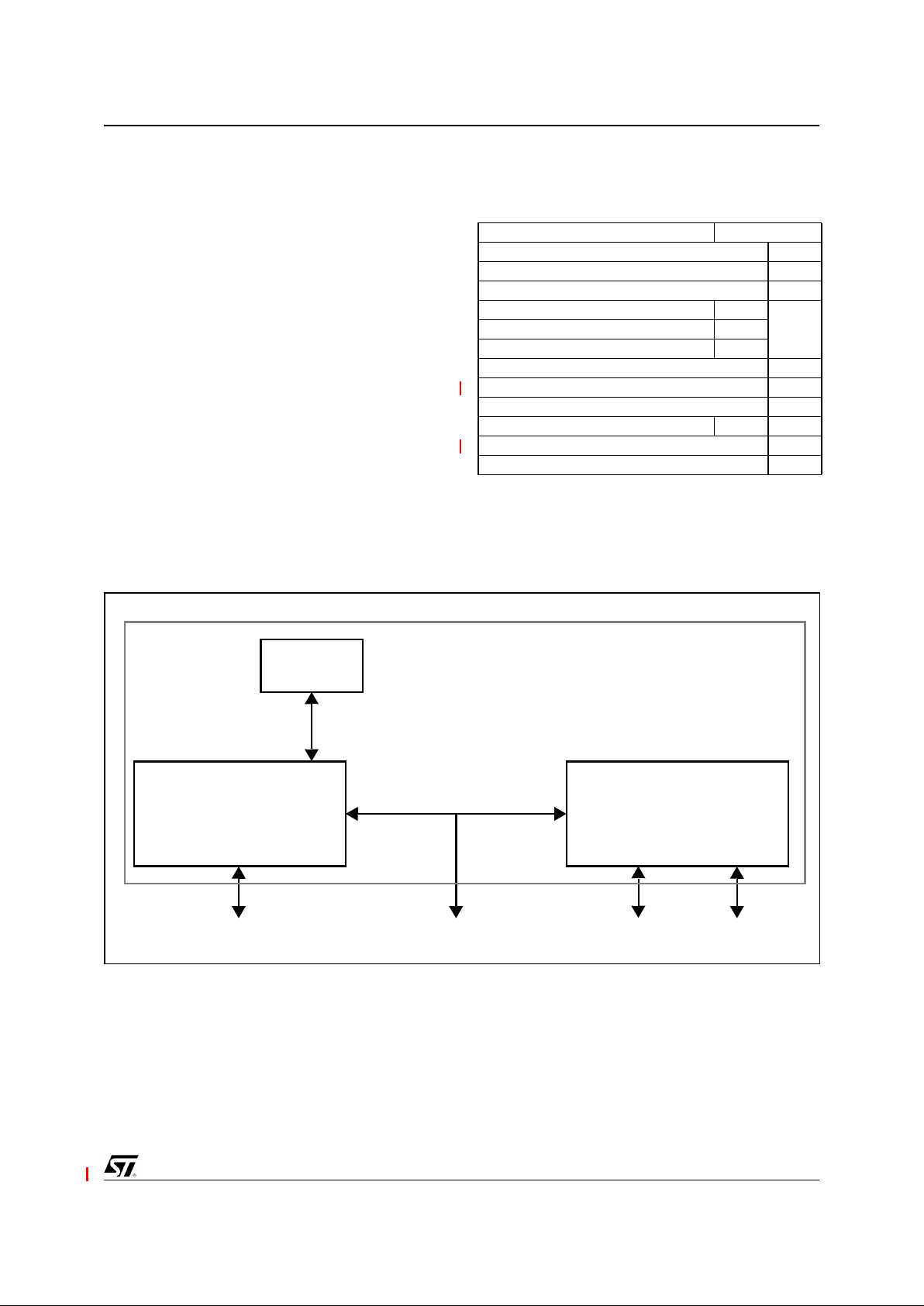
Table 1-1. Memory configurations
Memory
Bank size
Number
Organisa
tion
Device
Size
1Mx64 4 1Mx16
16Mbits2Mx64 8 2Mx8
4Mx64 16 4Mx4
4Mx64 4 2Mx16x2
64Mbits
8Mx64 8 4Mx8x2
16Mx64 16 8Mx4x2
4Mx64 4 1Mx16x4
8Mx64 8 2Mx8x4
32Mx64 16 4Mx4x4
16Mx64 8 2Mx16x2
128Mbits
32Mx64 16 4Mx8x4
Page 6

GENERAL DESCRIPTION
6/87
Release 1.3 - Januar
y
29, 2002
This is preliminary information on a new product now in development or undergoing evaluation. Details are subject to change without notice.
- 3 power-down timers detecting system inactivity:
- Doze timer (short durations).
- Stand-by timer (medium durations).
- Suspend timer (long durations).
- House-keeping activity detection.
- House-keeping timer to cope with short bursts of
house-keeping activity while dozing or in stand-by
state.
- Peripheral activity detection.
- Peripheral timer detecting peripheral inactivity
- SUSP# modulation to adjust the system
performance in various power down state s of the
system including full power-on state.
- Power control outputs to disable power from
different planes of the board.
Lack of system activity for progressively longer
periods of time is detected by the three power
down timers. These timers can generate SMI
interrupts to CPU so that the SMM software can
put the system in decreasing states of power
consumption. Alternatively, system activity in a
power down state can g enerate an SMI interrupt
to allow the software to bring the system back up
to full power-on state. The chip-set supports up to
three power down states described above; these
correspond to decreasing levels of power savings.
Power down puts the STPC Elite into suspend
mode. The processor completes execution of the
current instruction, any pending decoded
instructions and associated bus cycles. During the
suspend mode, internal clocks are stopped.
Removing power-down, the processor resumes
instruction fetching and begins execution in the
instruction stream at the point it had stopped.
Because of the static nature of the core, no
internal data is lost.
1.3. JTAG
JT A G stands for Joint Test Action Group and is the
popular name for IEEE Std. 1149.1, Standard T est
Access Port and Boundary-Scan Architec-ture.
This built-in circuitry is used to assist in the test,
maintenance and support of functional circuit
blocks. The circuitry includes a standard interface
through which instructions and test data are
communicated. A set of test features is defined,
including a boundary-scan registe r so that a
component is able to respond to a minimum set of
test instructions.
Page 7
GENERAL DESCRIPTION
Release 1.3 - January 29, 2002 7/87
This is preliminary information on a new product now in development or undergoing evaluation. Details are subject to change without notice.
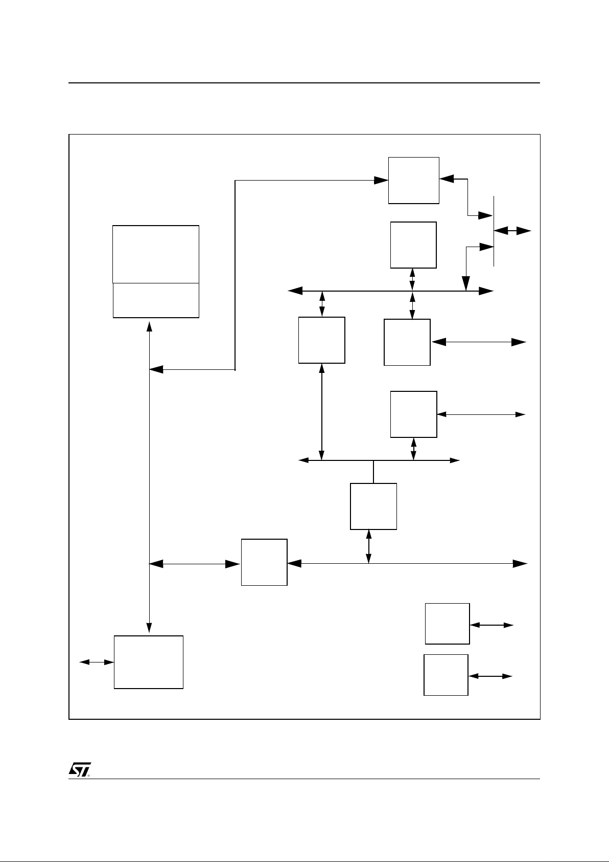
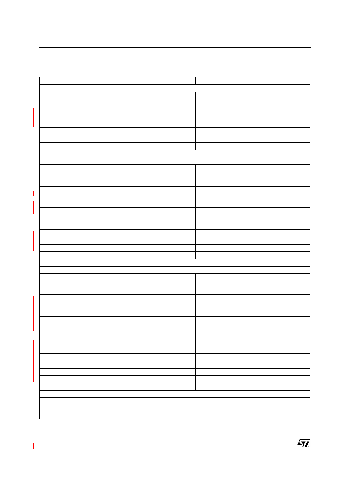
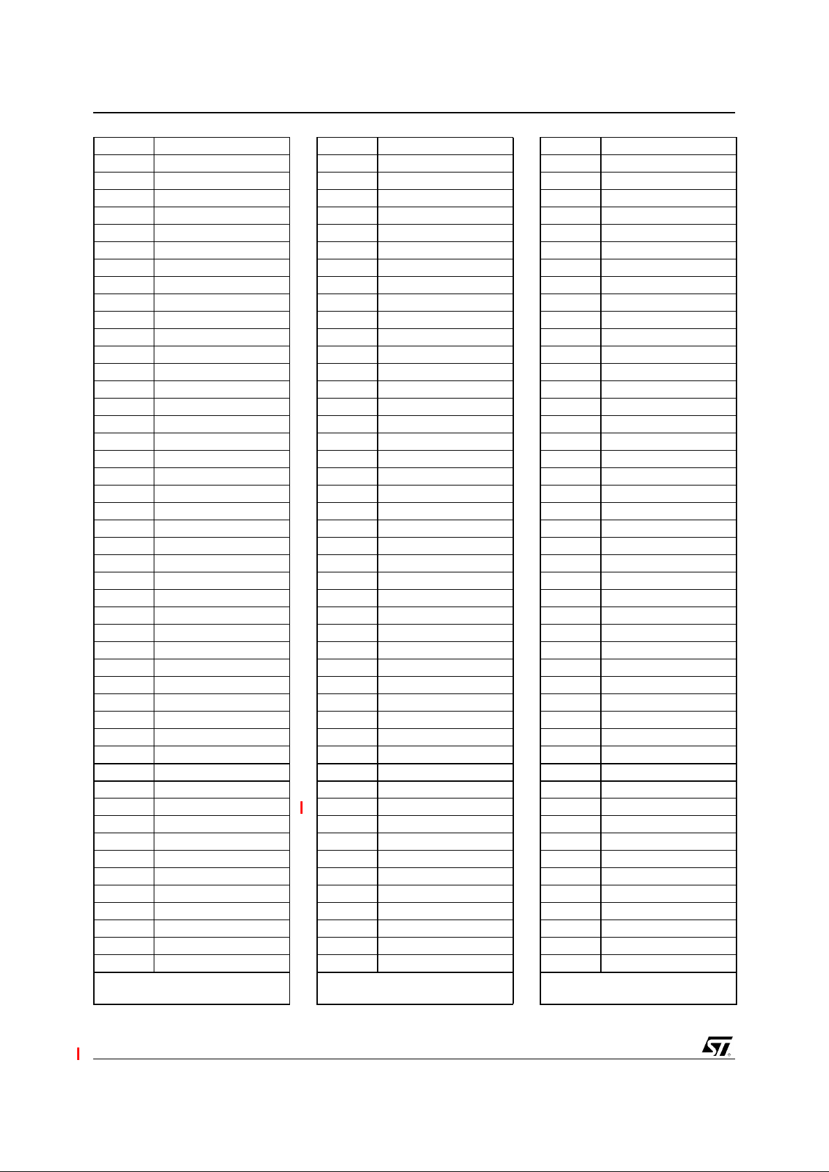
Figure 1-1. Functional description.
PCI North
Bridge
Host I/F
X86
Core
SDRAM
Controller
ISA
m/s
EIDE
PCI South
Bridge
ISA BUS
IPC
82C206
EIDE
GPIO
x16
Local
Bus I/F
JTAG
LOCAL BUS
GPCLK
Page 8
GENERAL DESCRIPTION
8/87
Release 1.3 - Januar
y
29, 2002
This is preliminary information on a new product now in development or undergoing evaluation. Details are subject to change without notice.
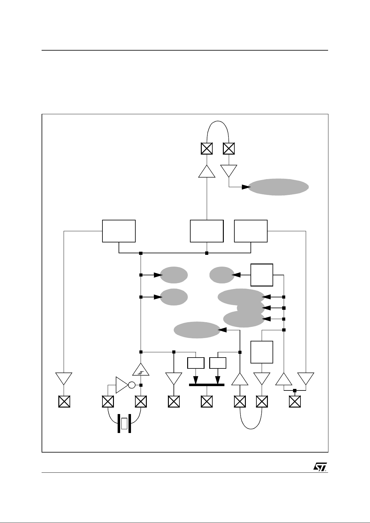
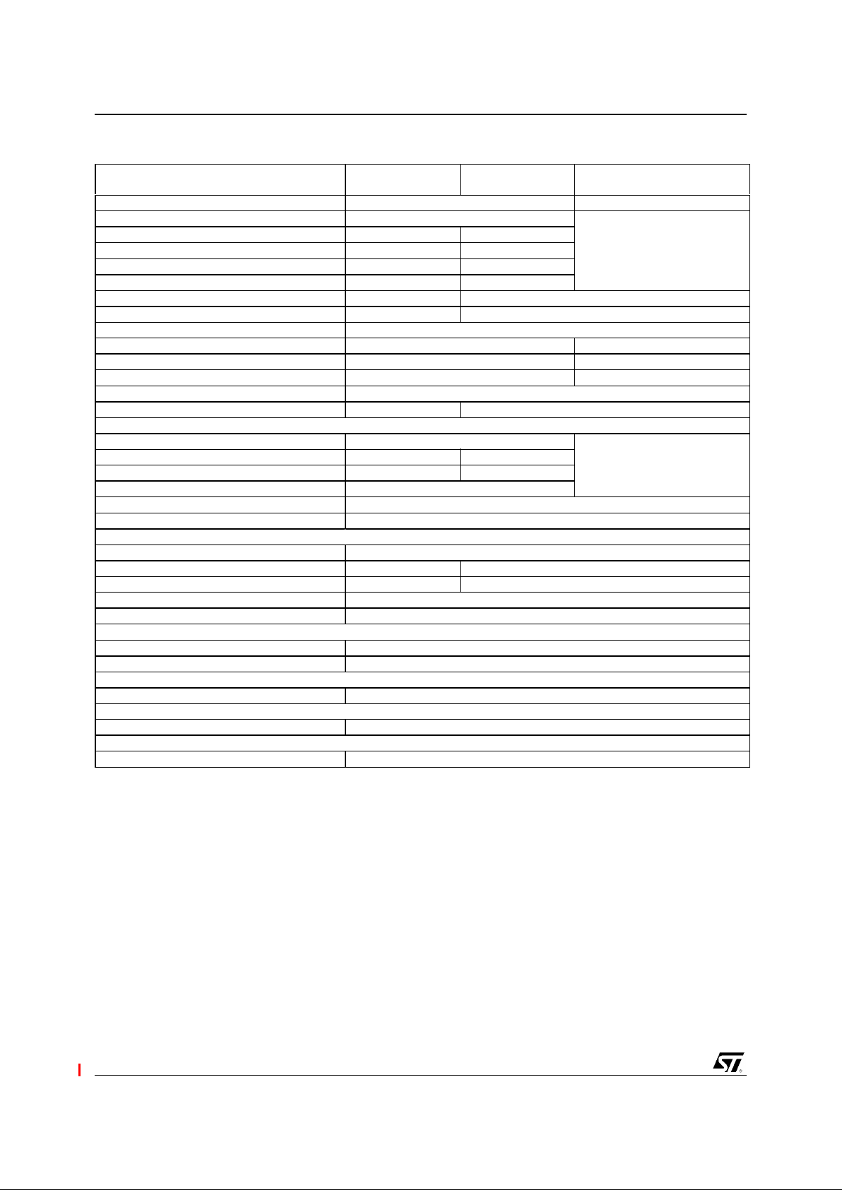
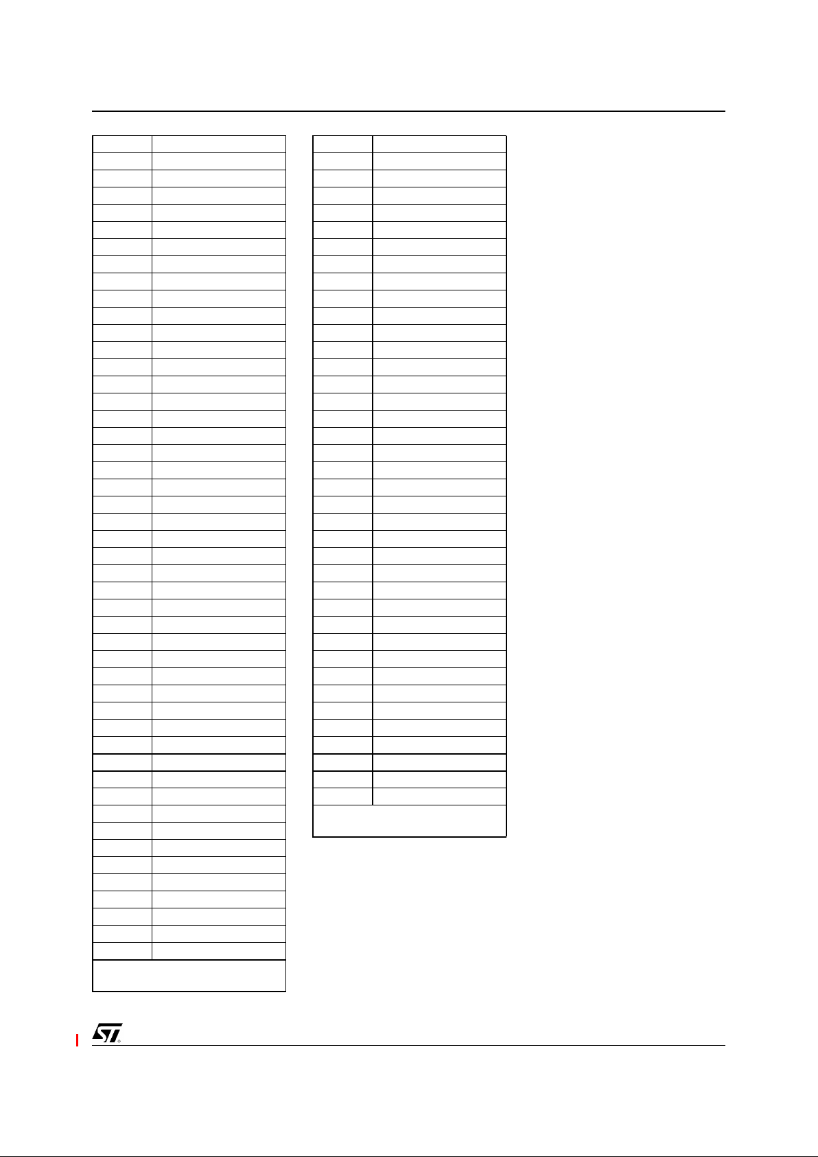
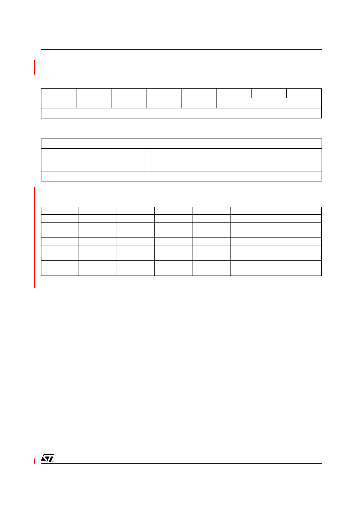
1.4. CLOCK TREE
The STPC Elite integrates many features and
generates all its clocks from a single 14MHz
oscillator. This results in multiple clock domains as
described in Figure 1-2.
The speed of the PLLs is either fixed (DE VCLK),
either programmable by strap option (HCLK)
either programmable by software (GPCLK,
MCLK). When in synchronized mode, MCLK
speed is fixed to HCLKO speed and HCLKI is
generated from MCLKI.
Figure 1-2. STPC Elite clock architecture
IPC
SDRAM controller
North Bridge
14.31818 MHz
XTALO XTALI
OSC14M ISACLK
1/4
GPCLK
GPCLK
PLL
(14MHz)
1/2
HCLK
PLL
PCICLKI PCICLKO
South Bridge
1/2
1/3
HCLK
MCLK
PLL
MCLKIMCLKO
CPU
x1
x2
Local Bus
Host
ISA
HCLKI
HCLKO
Page 9
GENERAL DESCRIPTION
Release 1.3 - January 29, 2002 9/87
This is preliminary information on a new product now in development or undergoing evaluation. Details are subject to change without notice.
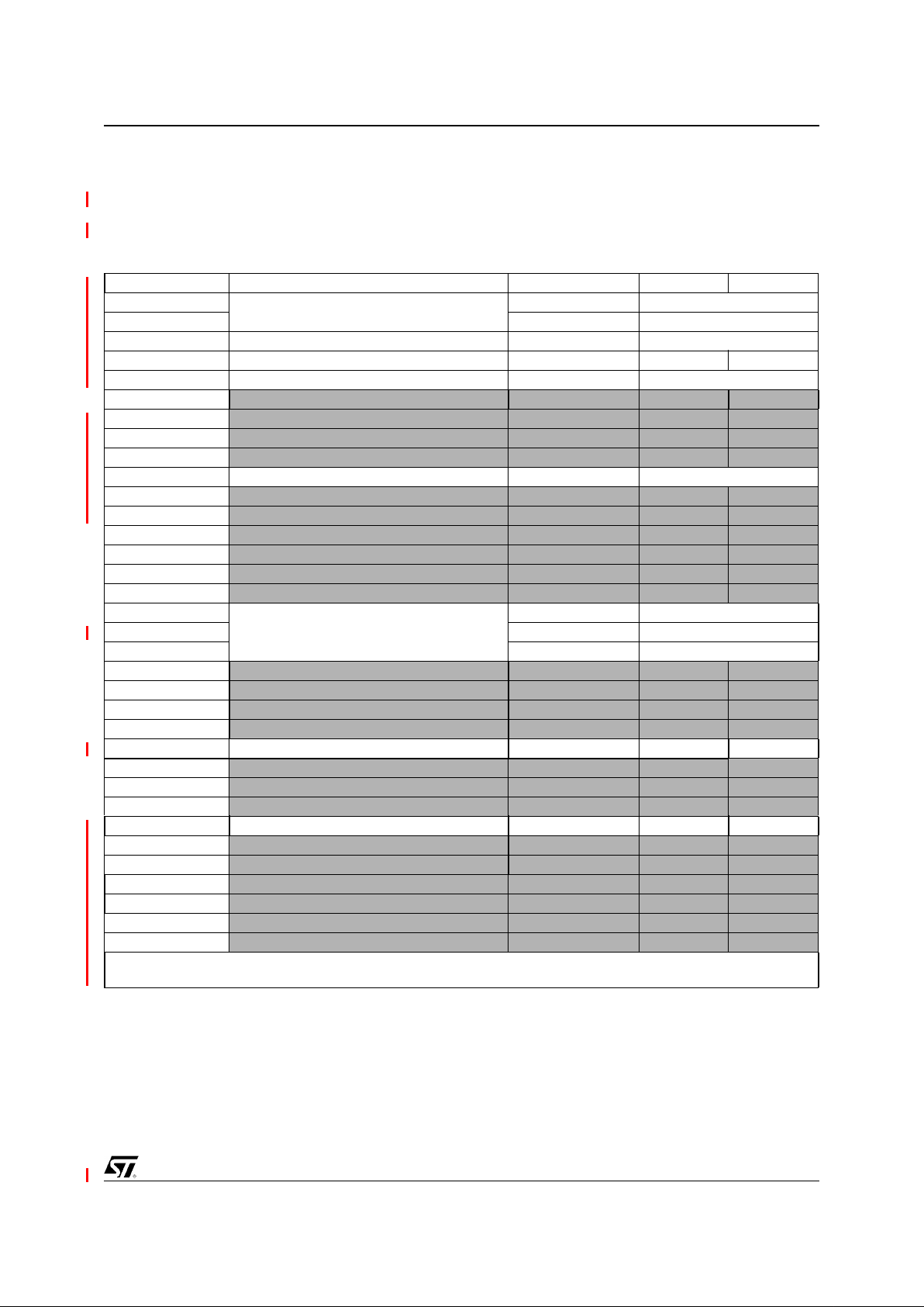
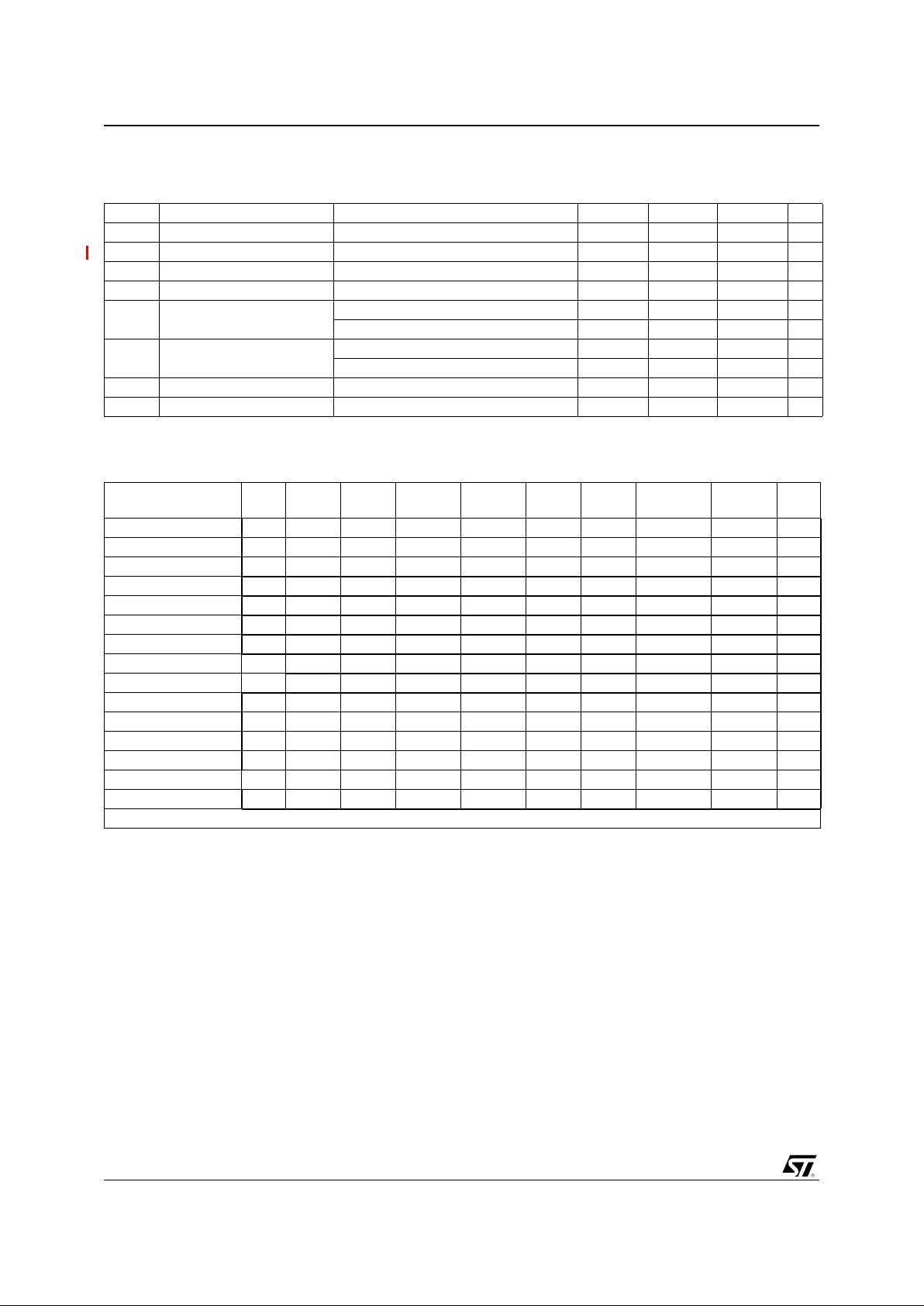
Figure 1-3. Typical ISA-based Application.
STPC Elite
ISA
PCI
4x 16-bit SDRAMs
Super I/O
2x EIDE
Flash
Keyboard / Mouse
Serial Ports
Parallel Port
Floppy
IRQ
DMA.REQ
DMA.ACK
DMUX
DMUX
MUX
MUX
RTC
GPIOs
GPCLK
Page 10

GENERAL DESCRIPTION
10/87
Release 1.3 - Januar
y
29, 2002
This is preliminary information on a new product now in development or undergoing evaluation. Details are subject to change without notice.
Page 11
PIN DESCRIPTION
Release 1.3 - January 29, 2002 11/87
This is preliminary information on a new product now in development or undergoing evaluation. Details are subject to change without notice.
2. PIN DESCRIPTION
2.1. INTRODUCTION
The STPC Elite integrates most of the
functiona lities of the PC archite cture. A s a resu lt,
many of the traditional interconnections between
the host PC microprocessor and the peripheral
devices are totally internal to the STPC Elite. This
offers improved performance due to the tight
coupling of the processor core and these
peripherals. As a result many of the external pin
connections are made directly to the on-chip
peripheral functions.
Figure 2-1 shows the STPC Elite external
interfaces. It defines the main buses and their
function. Table 2-1 describes the physical
implementation listing signals type and their
functionality. Table 2-2 provides a full pin listing
and description of pins. Table 2-7 provides a full
listing of pin locations of the STPC Elite package
by physical connection.
Note:
Several interface pins are multiplexed with
other functions, refer to Table 2-4 and Table 2-5
for further details
Table 2-1. Signal Description
Group name Qty
Basic Clocks reset & Xtal 6
Memory Interface 96
PCI interface 56
ISA 79
90IDE 34
Local Bus 50
Grounds 69
V
DD
22
Miscellaneous 8
GPIO 16
Unconnected 25
Total Pin Count 388
Figure 2-1. STPC Elite External Interfaces
SOUTHNORTH PCI
x86
SDRAM I/F
SYS
ISA/IDE/LB
96 56
6
90
STPC Elite
Page 12
PIN DESCRIPTION
12/87
Release 1.3 - Januar
y
29, 2002
This is preliminary information on a new product now in development or undergoing evaluation. Details are subject to change without notice.
Table 2-2 . Def i ni t io n of Si gn a l Pin s
Signal Name Dir Buffer Type
2
Description Qty
BASIC CLOCKS AND RESETS
SYSRSETI# I SCHMITT_FT System Power Good Input 1
SYSRSTO# O BD8STRP_FT System Reset Output 1
XTALI I ANA
14.3 MHz Crystal Input - External
Oscillator Input
1
XTALO I/O OSCI13B 14.3 MHz Crystal Output 1
HCLK I/O BD4STRP_FT Host Clock (Test) 1
GP_CLK O BT8TRP_TC General Purpose Clock 1
V
DD
_xxx_PLL
1
Power Supply for PLL Clocks
MEMORY INTERFACE
MCLKI I TLCHT_TC Memory Clock Input 1
MCLKO O BT8TRP_TC Memory Clock Output 1
CS#[1:0] O BD8STRP_TC DIMM Chip Select 2
CS#[3]/MA[13]/BA[1] O BD16STARUQP_TC
DIMM Chip Select/ Memory Address/
Bank Address
1
CS#[2]/MA[12] O BD16STARUQP_TC DIMM Chip Select/ Bank Address 1
MA[10:0] O BD16STARUQP_TC Memory Row & Column Address 12
MD[48:10], [7:2] I/O BD8TRP_TC Memory Data 45
MD[63:49], [9:8], [1:0] I/O BD8STRUP_FT Memory Data 19
RAS#[1:0] O BD16STARUQP_TC Row Address Strobe 2
CAS#[1:0] O BD16STARUQP_TC Column Address Strobe 2
MWE# O BD16STARUQP_TC Write Enable 1
DQM[7:0] O BD8STRP_TC Data Input/Output Mask 8
PCI INTERFACE
PCI_CLKI I TLCHT_FT 33 MHz PCI Input Clock 1
PCI_CLKO O BT8TRP_TC
33 MHz PCI Output Clock (from internal
PLL)
1
AD[31:0] I/O BD8PCIARP_FT PCI Address / Data 32
CBE[3:0] I/O BD8PCIARP_FT Bus Commands / Byte Enables 4
FRAME# I/O BD8PCIARP_FT Cycle Frame 1
IRDY# I/O BD8PCIARP_FT Initiator Ready 1
TRDY# I/O BD8PCIARP_FT Target Ready 1
LOCK# I TLCHT_FT PCI Lock 1
DEVSEL# I/O BD8PCIARP_FT Device Select 1
STOP# I/O BD8PCIARP_FT Stop Transaction 1
PAR I/O BD8PCIARP_FT Parity Signal Transactions 1
SERR# O BD8PCIARP_FT System Error 1
PCI_REQ#[2:0] I BD8PCIARP_FT PCI Request 3
PCI_GNT#[2:0] O BD8PCIARP_FT PCI Grant 3
PCI_INT[3:0] I BD4STRUP_FT PCI Interrupt Request 4
ISA CONTROL
Note
1
: These pins must be connected to the 2.5 V power supply. They
must not
be connected to the 3.3V supply.
Note
2
: See Table 2-3 for buffer type descriptions.
Page 13
PIN DESCRIPTION
Release 1.3 - January 29, 2002 13/87
This is preliminary information on a new product now in development or undergoing evaluation. Details are subject to change without notice.
ISA_CLK O BT8TRP_TC
ISA Clock Output - Multiplexer Select
Line For IPC
1
ISA_CLK2X O BT8TRP_TC
ISA Clock x2 Output - Multiplexer Select
Line For IPC
1
OSC14M O BD8STRP_FT Buffered 14MHz clock 1
LA[23:17] O BD8STRUP_FT Unlatched Address 7
SA[19:0] I/O BD8STRUP_FT Latched Address 20
SD[15:0] I/O BD8STRP_FT Data Bus 16
ALE O BD4STRP_FT Address Latch Enable 1
MEMR#, MEMW# I/O BD8STRUP_FT Memory Read and Memory Write 2
SMEMR#, SMEMW# O BD8STRUP_FT
System Memory Read and Memory
Write
2
IOR#, IOW# I/O BD8STRUP_FT I/O Read and Write 2
MCS16#, IOCS16# I BD4STRUP_FT Memory/IO Chip Select16 2
BHE# O BD8STRUP_FT System Bus High Enable 1
ZWS# I BD4STRP_FT Zero Wait State 1
REF# O BD8STRP_FT Refresh Cycle. 1
MASTER# I BD4STRUP_FT Add On Card Owns Bus 1
AEN O BD8STRUP_FT Address Enab le 1
IOCHCK# I BD4STRUP_FT I/O Channel Check. 1
IOCHRDY I/O BD8STRUP_ FT
I/O Channel Ready (ISA) - Busy/Ready
(IDE)
1
ISAOE# O B D4ST RP_F T ISA /IDE Selec tion 1
GPIOCS# I/O BD4STRP_FT General Purpose Chip Select 1
IRQ_MUX[3:0] I BD4STRP_FT Time-Multiplexed Interrupt Request 4
DREQ_MUX[1:0] I BD4STRP_FT Time-Multiplexed DMA Request 2
DACK_ENC[2:0] O BD4STRP_FT Encoded DMA Acknowledge 3
TC O BD4STRP_FT ISA Terminal Count 1
RTCAS O BD4STRP_FT Real Time Clock Address Strobe 1
RMRTCCS# I/O BD4STRP_FT ROM/RTC Chip Select 1
KBCS# I/O BD4STRP_FT Keyboard Chip Select 1
RTCRW# I/O BD4STRP_FT RTC Read/Write 1
RTCDS# I/O BD4STRP_FT RTC Data Strobe 1
LOCAL BUS
PA[23:20], [15], [8], [3:0] O BD4STRP_FT Address Bus 10
PA[19:16], [14:12],[7:4] O BD8STRUP_FT Address Bus 11
PA[11] O BD8STRP_F T Address Bus 1
PA[10:9] O BD4STRUP_FT Address Bus 2
PD[15:0] I/O BD8STRP_FT Data Bus 16
PRD1#,PRD0# O BD4STRUP_FT Peripheral Read Control 2
PWR1# O BD8STRUP_FT Peripheral Write Control 1
PWR0# O BD4STRUP_FT Peripheral Write Control 1
PRDY I BD8STRUP_FT Data Ready 1
FCS1#, FCS0# O BD4STRP_FT Flash Chip Select 2
IOCS#[3] O BD4STRP_FT I/O Chip Select 1
IOCS#[2:0] O BD8STRUP_FT I/O Chip Select 3
Table 2-2 . Def i ni t io n of Si gn a l Pin s
Signal Name Dir Buffer Type
2
Description Qty
Note
1
: These pins must be connected to the 2.5 V power supply. They
must not
be connected to the 3.3V supply.
Note
2
: See Table 2-3 for buffer type descriptions.
Page 14
PIN DESCRIPTION
14/87
Release 1.3 - Januar
y
29, 2002
This is preliminary information on a new product now in development or undergoing evaluation. Details are subject to change without notice.
IDE CONTROL
DA[2:0] O BD8STRUP_ FT Add ress Bus 3
DD[15:12] I/O BD4STRP_FT Data Bus 4
DD[11:0] I/O BD8STRUP_FT Data Bus 12
PCS3#,PCS1#,SCS3#,SCS1# O BD8STRUP_FT Primary & Secondary Chip Selects 4
DIORDY O BD8STRUP_FT Data I/O Ready 1
PIRQ, SIRQ I BD4STRP_FT Primary & Secondary Interrupt Request 2
PDRQ, SDRQ I BD4STRP_FT Primary & Secondary DMA Request 2
PDACK#, SDACK# O BD8STRP_FT
Primary & Secondary DMA
Acknowledge
2
PDIOR#, SDIOR# O BD8STRUP_FT Primary & Secondary I/O Channel Read 2
PDIOW#, SDIOW# O BD8STRP_FT Primary & Secondary I/O Channel Write 2
MISCELLANEOUS
GPIO[15:0] I/O BD4ST RP_F T General Purpose I/Os 16
SPKRD O BD4STRP_FT Speaker Device Output 1
SCL I/O BD4STRUP_FT
I²C Interface - Clock / Can be used for
VGA DDC[1] signal
1
SDA I/O BD4STRUP_FT
I²C Interface - Data / Can be used for
VGA DDC[0] signal
1
SCAN_ENABLE I TLCHTD_TC Reserved (Test pin) 1
TCLK I BD4STRP_FT Test clock 1
TDI I BD4STRP_FT Test data input 1
TMS I BD4STRP_FT Test mode input 1
TDO O BD4STRP_FT Test data output 1
Table 2-2 . Def i ni t io n of Si gn a l Pin s
Signal Name Dir Buffer Type
2
Description Qty
Note
1
: These pins must be connected to the 2.5 V power supply. They
must not
be connected to the 3.3V supply.
Note
2
: See Table 2-3 for buffer type descriptions.
Page 15
PIN DESCRIPTION
Release 1.3 - January 29, 2002 15/87
This is preliminary information on a new product now in development or undergoing evaluation. Details are subject to change without notice.
Table 2-3. Buffer Type Descriptions
Buffer Description
ANA Analog pad buffer
OSCI13B Oscillator, 13 MHz, HCMOS
BT8TRP_TC LVTTL Bi-Directional, 8 mA drive capability, Schmitt trigger
BD4STRP_FT LVTTL Bi-Directional, 4 mA drive capability, Schmitt trigger, 5V tolerant
BD4STRUP_FT LVTTL Bi-Directional, 4 mA drive capability, Schmitt trigger, Pull-Up, 5V tolerant
BD8STRP_FT LVTTL Bi-Directional, 8 mA drive capability, Schmitt trigger, 5V tolerant
BD8STRUP_FT LVTTL Bi-Directional, 8 mA drive capability, Schmitt trigger, Pull-Up, 5V tolerant
BD8STRP_TC LVTTL Bi-Directional, 8 mA drive capability, Schmitt trigger
BD8TRP_TC LVTTL Bi-Directional, 8 mA drive capability, Schmitt trigger
BD8PCIARP_FT LVTTL Bi-Directional, 8 mA drive capability, PCI compatible, 5V tolerant
BD16STARUQP_TC LVTTL Bi-Directional, 16 mA drive capability, Schmitt trigger
SCHMITT_FT LVTTL Input, Schmitt trigger, 5V tolerant
TLCHT_FT LVTTL Input, 5V tolerant
TLCHT_TC LVTTL Input
TLCHTD_TC LVTTL Input, Pull-Down
Page 16

PIN DESCRIPTION
16/87
Release 1.3 - Januar
y
29, 2002
This is preliminary information on a new product now in development or undergoing evaluation. Details are subject to change without notice.
2.2. SIGNAL DESCRIPTIONS
2.2.1. BASIC CLOCKS AND RESETS
SYSRSTI#
System Reset/Power good.
This input
is low when the reset switch is depressed.
Otherwise, it reflects the power supply’s power
good signal. This input is asynchronous to all
clocks, and acts as a negative active reset. The
reset circuit initiates a hard reset on the rising
edge of this signal.
SYSRSTO#
Rese t Outpu t to System .
This is the
system reset signal and is used to r eset the rest of
the components (not on Host bus) in the system.
The ISA bus reset is an externally inverted
buffered version of this output and the PCI bus
reset is an externally buffered version of this
output.
XTALI
14.3 MHz Crystal Input
XTALO
14.3 MHz Crystal Output.
These pins are
provided for the connection of an external 14.318
MHz crystal to provide the reference clock for the
internal frequency synthesizer, from which all
other clock signals are generated.
The 14.318 MHz series-cut fundamental (not
overtone) mode quartz crystal must have an
Equivalent Series Resistance (ESR, sometimes
referred to as Rm) of less then 50 Ohms (typically
8 Ohms) and a shunt capacitance (Co) of less
than 7 pF. Balance capacitors of 16 pF should
also be added, one connected to each pin.
In the event of an ext ernal o scillat or pr ovidin g the
master clock signal to the STPC Elite device, the
TTL signal should be connected to XTALI.
HCLK
Host Clock.
This clock supplies the CPU
and the host related blocks. This clock can e
doubled inside the CPU and is intended to operate
in the range of 25 to 100 MHz. This clock in
generated internally from a PLL bu t can be driven
directly from the extern a l syst e m.
GP_CLK
General Purpose clock.
This clock is
programmable and its frequency can be as high
as 135 MHz.
2.2.2. MEMORY INTERFACE
MCLKI
Memory Clock Input.
This clock is driving
the SDRAM controller. This input should be a
buffered version of the MCLKO when more than 4
SDRAM chips are used. Go to section 6.3 for
more details.
MCLKO
Memory Clock Output.
This clock is
driving the SDRAM devices and is generated from
an internal PLL. The default value is 66 MHz.
CS#[2]/MA[11]
Chip Select/ Bank Address
This
pin is CS#[2] in the case when 16 Mbit devices are
used. For all other densities, it becomes MA[11].
CS#[3]/MA[12]/BA[1]
Chip Select/ Memory
Address/ Bank Address
This pin is CS#[3] in the
case when 16Mbit devices are used. For all other
densities, it becomes MA[12] when 2 internal
banks devices are used and BA[1] when 4 internal
bank devices are used.
MA[10:0]
Memory Address.
Multiplexed row and
column address lines.
BA[0]
Memory Bank Address.
CS#[1:0]
Chip Se lect.
These signals a re used to
disable or enable device operation by masking or
enabling all SDRAM inputs except MCLK, CKE,
and DQM.
MD[63:0]
Memory Dat a.
This is the 64-bit memory
data bus. MD[40-0] are read by the device strap
option registers during rising edge of SYSRSTI#.
RAS#[1:0]
Row Address Strobe.
There are two
active-low row address strobe output signals. The
RAS# signals drive the memory devices directly
without any external buffering.
CAS#[1:0]
Column Address Strobe.
There are
two active-low column address strobe output
signals. The CAS# signals drive the memory
devices directly without any external buffering.
MWE#
Write Enable.
Write enable specifies
whether the memory access is a read (MWE# = H)
or a write (MWE# = L).
DQM#[7:0]
Data Mask.
Makes data output Hi-Z
after the clock and masks the SDRAM outputs.
Blocks SDRAM data input when DQM active.
2.2.3. PCI INTERFACE
PCI_CLKI
33 MHz PCI Input Clock .
This signal is
the PCI bus clock input and should be driven from
the PCI_CLKO pin.
PCI_CLKO
33 MHz PCI Output Clock .
This is t h e
master PCI bus clock output.
AD[31:0]
PCI Address/Data.
This is the 32-bit
multiplexed address and data bus of the PCI. This
bus is driven by the master during the address
phase and data phase of write transactions. It is
driven by the target during data phase of read
transactions.
CBE#[3:0]
Bus Commands/Byte Ena bles.
These
are the multiplexed command and byte enable
signals of the PCI bus. During the address phase
they define the command and during the data
Page 17

PIN DESCRIPTION
Release 1.3 - January 29, 2002 17/87
This is preliminary information on a new product now in development or undergoing evaluation. Details are subject to change without notice.
phase they carry the byte enable information.
These pins are inputs when a PCI master other
than the STPC Elite owns the bus and outputs
when the STPC Elite owns the bus.
FRAME#
Cycle Frame.
This is the frame signal of
the PCI bus. It is an input when a PCI master owns
the bus and is an output when STPC Elite owns
the PCI bus.
IRDY#
Initiator Ready.
This is the initiator ready
signal of the PCI bus. It is used as an output when
the STPC Elite initiates a bus cycle on the PCI
bus. It is used as an input during the PCI cycles
targeted to the STP C Eli te to determine when the
current PCI master is ready to complete the
current transact i o n.
TRDY#
Target Ready.
This is the target ready
signal of the PCI bus. It is driven as an output
when the STPC Elite is the target of the current
bus transaction. It is used as an input when STPC
Elite initiates a cycle on the PCI bus.
LOCK#
PCI Lock.
This is the lock signal of the PCI
bus and is used to implement the exclusive bus
operations when acting as a PCI target agent.
DEVSEL#
I/O Device Select.
This signal is used
as an input when the STPC E lite initiates a bus
cycle on the PCI bus to determine if a PCI slave
device has decoded itself to be the target of the
current transaction. It is asserted as an output
either when the STPC Elite is the target of the
current PCI transaction or when no other device
asserts DEVSEL# prior to the subtractive decode
phase of the current PCI transaction.
STOP#
Stop Transaction.
Stop is used to
implement the disconnect, retry and abort protocol
of the PCI bus. It is used as an input for the bus
cycles initiated by the S TPC Elite and is used as
an output when a PCI master cycle is t argeted to
the STPC Elite .
PAR
Parity Signal Transactions.
This is the pa rity
signal of the PCI bus. This signal is used to
guarantee even parity across AD[31:0],
CBE#[3:0], and PAR. Thi s signal is driven by the
master during the address phase and data phase
of write transactions. It is driven by the target
during data phase of read transactions. (Its
assertion is identical to that of the AD bus delayed
by one PCI clock cycle)
SERR#
System Error.
This is the system error
signal of the PCI bus. It may, if enabled, be
asserted for one PCI clock cycle if target aborts a
STPC Elite in itiated PCI t ransaction. I ts assertion
by either the STPC Elite or by another PCI bus
agent will trigger the assertion of NMI to the host
CPU. This is an open drain output.
PCI_REQ#[2:0]
PCI Request.
This pin are the
three external PCI master request pins. They
indicates to the PCI arbiter that the external
agents desire use of the bus.
PCI_GNT#[2:0]
PCI Grant.
These pins indicate
that the PCI bus has been g ranted to the master
requesting it on its PCIREQ#.
PCI_INT[3:0]
PCI Interrupt Request.
These are
the PCI bus interrupt signals.
2.2.4. ISA INTERFACE
ISA_CLK, ISA_CLKX2
ISA Clock x1, x2.
These
pins generate the Clock signal for the ISA bus and
a Doubled Clock signal. They are also used as the
multiplexer control lines for the Interrupt Controller
Interrupt input lines. ISA_CLK is generated from
either PCICLK/4 or OSC14M/ 2.
OSC14M
ISA bus synchronisation clock Output.
This is the buffered 14.318 MHz clock for the ISA
bus.
LA[23:17]
Unlatched Address.
When the ISA bus
is active, these pins are ISA Bus unlatched
address for 16-bit devices. When ISA bus is
accessed by any cycle initiated from PCI bus,
these pins are i n o utput mode. When an ISA bus
master owns the bus, these pins are in input
mode.
SA[19:0]
ISA Address Bus.
System address bus
of ISA on 8-bit slot. These pins are used as an
input when an ISA bus master o wns the bus and
are outputs at all other times.
SD[15:0]
I/O Data Bus.
These pins are the
external databus to the ISA bus.
ALE
Address Latch En able.
This is the address
latch enable output of the ISA bus and is asserted
by the STPC Elite to indicate that LA23-17, SA190, AEN and SBHE# signals are valid. The ALE is
driven high during refresh, DMA master or an ISA
master cycles by the STPC Elite. ALE is driven
low after re se t.
MEMR#
Memory Read.
This is the memory read
command signal of the IS A bus. It is used as an
input when an ISA master owns the bus and is an
output at all other times.
The MEMR# signal is active during refresh.
MEMW#
Memory Write.
This is the memory write
command signal of the IS A bus. It is used as an
input when an ISA master owns the bus and is an
output at all other times.
SMEMR#
System Memory Read.
The STPC Elite
generates SMEMR# signal of the ISA bus only
Page 18

PIN DESCRIPTION
18/87
Release 1.3 - Januar
y
29, 2002
This is preliminary information on a new product now in development or undergoing evaluation. Details are subject to change without notice.
when the address is bel ow one megabyte or the
cycle is a refresh cycle.
SMEMW#
System Me mory Write.
The STPC Eli te
generates SMEMW# signal of the ISA bus only
when the address is below one megabyte.
IOR#
I/O Read.
This is the IO read command
signal of the ISA bus. It is an input when an ISA
master owns the bus an d is an out put at al l other
times .
IOW#
I/O Write.
This is the IO write command
signal of the ISA bus. It is an input when an ISA
master owns the bus an d is an out put at al l other
times .
MCS16#
Memory Chip Select16.
This is the
decode of LA23-17 address pins of the ISA
address bus without any qualification of the
command signal lines. MCS16# is always an
input. The STPC Elite ignores this signal during IO
and refresh cycles.
IOCS16#
IO Chip Select16.
This signal is the
decode of SA15-0 address pins of the ISA
address bus without any qualification of the
command signals. The STPC Elite doe s not drive
IOCS16# (similar to PC-AT design). An ISA
master access to an internal registe r of the S TPC
Elite is executed as an extended 8-bit IO cycle.
BHE#
System Bus High Enable.
This signal, when
asserted, indicates that a data byte is being
transferred on SD15-8 lines. It is used as an input
when an ISA master owns the bus and is an
output at all other times.
ZWS#
Zero Wait Stat e.
This signal, when asserted by addressed device, indicates that current cycle can be shortened.
REF#
Refresh Cycle.
This is the refresh command
signal of the ISA bus. It is driven as an output
when the STPC Elite perf orms a refresh cycle on
the ISA bus. It is used as an input when an ISA
master owns the bus and is used to trigger a
refresh cycle.
The STPC Elite performs a pseudo hidden
refresh. It requests the host bus for two host
clocks to drive the refresh address and capture it
in external buffers. The host bus is then
relinquished while the refresh cycle continues on
the ISA bus.
MASTER#
Add On Card Owns Bus.
This signal is
active when an ISA device h as been granted bus
ownership.
AEN
Address Enable.
Address Enable is enabl ed
when the DMA controller is the bus owner to
indicate that a DMA transfer will occur. The
enabling of the signal indicat es to IO devices to
ignore the IOR#/IOW# signal during DMA
transfers.
IOCHCK#
IO Channel Che ck.
IO Channel Check
is enabled by any ISA device to signal an error
condition that can not be corrected. NMI signal
becomes active upon seeing IOCHCK# active if
the corresponding bit in Port B is enabled.
IOCHRDY
Channel Ready.
IOCHRDY is the IO
channel ready signal of the ISA bus and is driven
as an output in response to an ISA master cycle
targeted to the host bus or an internal register of
the STPC Elite. The STPC Elite monitors this
signal as an input when performing an ISA cycle
on behalf of the host CPU, DMA master or refresh.
ISA masters which do not monitor IOCHRDY are
not guaranteed to work with the STPC Elite since
the access to the system memory can be
considerably delayed due UMA architecture.
ISAOE#
Bidirectional OE Control.
This signal
controls the OE
signal of the external transceiver
that connects the IDE DD bus and ISA SA bus.
GPIOCS#
I/O General Purpo se Chip Select .
This
output signal is used by the external la tch on ISA
bus to latch the data on the SD[7:0] bus. The latch
can be use by PMU unit to control the external
peripheral devices or any other desired function.
IRQ_MUX[3:0]
Multiplexed Interrupt Request.
These are the ISA bus interrupt signals. They
have to be encoded before connection to the
STPC Elite using ISACLK and ISACLKX2 as the
input selection strobes.
Note that IRQ8B, which by convention is
connected to the RTC, is inverted before being
sent to the interrupt c ontroller, so that it may be
connected directly to the IRQ
pin of the RTC.
DREQ_MUX[1:0]
ISA Bus Multiplexed DMA
Request.
These are the ISA bus DMA request
signals. They are to be encoded before
connection to the STPC Elite us ing ISACLK and
ISACLKX2 as the input selection strobes.
DACK_ENC[2:0]
DMA Acknowledge.
These are
the ISA bus DMA ac knowledge sig nals. They are
encoded by the STPC Elite before output and
should be decoded ext ernally using ISACLK and
ISACLKX2 as the control strobes.
TC
ISA Terminal Count.
This is the terminal count
output of the DMA controller and is connected to
the TC line of the ISA bus. It is asserted during the
last DMA transfer, when the byte count expires.
2.2.5. X- BUS IN TERFACE PINS
RTCAS
Real time clock address strobe.
This
signal is asserted for any I/O write to port 70H.
Page 19

PIN DESCRIPTION
Release 1.3 - January 29, 2002 19/87
This is preliminary information on a new product now in development or undergoing evaluation. Details are subject to change without notice.
RMRTCCS#
ROM/Real Time clock chip select.
This signal is asserted if a ROM access is
decoded during a memory cycle. It should be
combined with MEMR# or MEMW# signals to
properly access the ROM. During a IO cycle, this
signal is asserted if access to the Real Time Clock
(RTC) is decoded. It should be combined with IOR
or IOW# signals to properly acces s the real time
clock.
KBCS#
Keyboard Chip Select.
This signal is
asserted if a keyboard access is decoded during a
I/O cycle.
RTCRW#
Real Time Clock RW.
This pin is a multifunction pin. When ISAOE# is active, this signal is
used as RTCRW#. This signal is asserted for any
I/O write to port 71H.
RTCDS#
Real Time Clock DS
. This pin is a multifunction pin. When ISAOE# is active, this signal is
used as RTCDS# This signal is asserted for any I/
O read to port 71H. Its polarity complies with the
DS pin of the MT48T86 RTC device when
configured with Intel timings.
Note: RMRTCCS#, KBCS#, RTCRW# and
RTCDS# signals must be ORed externally with
ISAOE# and then connected to the external
device. An LS244 or equivalent function can be
used if OE# is connected to ISAOE# and the
output is provided with a weak pull-up resistor as
shown in Design Guidelines chapter.
2.2.6. LOCAL BUS
PA[23:0]
Address Bus Output.
PD[15:0]
Data Bus.
This is the 16-bit data bus.
D[7:0] is the LSB and PD[15:8] is the MSB.
PRD#[1:0]
Read Control output.
PRD0# is used to
read the LSB and PRD1# to read the MSB.
PWR#[1:0]
Write Control output.
PWR0# is used
to write the LSB and PWR1# to write the MSB.
PRDY
Data Ready input.
This signal is used to
create wait states on the bus. When high, it
completes the current cycle.
FCS#[1:0]
Flash Chip Select output.
These are
the Programmable Chip Select signals for up to 2
banks of Flash memory.
IOCS#[3:0]
I/O Chip Select output.
These are the
Programmable Chip Select signals for up to 4
external I/O devices.
2.2.7. IDE INTERFACE
DA[2:0]
Address.
These signals are connected to
DA[2:0] of IDE devices directly or through a buffer.
If the toggling of sign als are t o be m asked du ring
ISA bus cycles, they can be externally ORed with
ISAOE# before being connected to the IDE
devices.
DD[15:0]
Databus.
When the IDE bus is active,
they serve as IDE signals D D[11:0]. IDE devices
are connected to SA[19:8] directly and ISA bus is
connected to these pins through two LS245
transceivers as described in Design Guidelines
chapter.
PCS1#, PCS3#
Primary Chip Select.
These
signals are used as the active high primary master
& slave IDE chip select signals. These signals
must be externally ANDed with the ISAOE
#
signal
before driving the I DE devices to guarantee it is
active only when ISA bus is idle.
SCS1#, SCS3#
Secondary Chip Select.
These
signals are used as the active high secondary
master & slave IDE chip select signals. These
signals must be externally ANDed with the
ISAOE
#
signal before driving the IDE devices to
guarantee it is active only when ISA bus is idle.
DIORDY
Busy/Ready.
This pin serves as IDE
signal DIORDY.
PIRQ
Primary Interrupt Request.
SIRQ
Secondary Interrupt Request.
Interrupt request from IDE channels.
PDRQ
Primary DMA Request.
SDRQ
Secondary DMA Request.
DMA request from IDE channels.
PDACK#
Primary DMA Acknowledge.
SDACK#
Secondary DMA Acknowledge.
DMA acknowledge to IDE channels.
PDIOR#, PDIOW#
Primary I/O Read & Write.
SDIOR#, SDIOW#
Secondary I/O Read & Write
.
Primary & Secondary channel read & write.
2.2.8. JTAG INTERFACE
TCLK
Test clock
TDI
Test data input
TMS
Test mode input
TDO
Test data output
2.2.9. MISCELLANEOUS
GPIO[15:0]
General Purpose I/Os
SPKRD
Speaker Drive.
This the output to the
speaker and is an AND of the counter 2 output
with bit 1 of Port 61, and dri ves an external speak-
Page 20

PIN DESCRIPTION
20/87
Release 1.3 - Januar
y
29, 2002
This is preliminary information on a new product now in development or undergoing evaluation. Details are subject to change without notice.
er driver. This output should be connected to 7407
type high voltage driver.
SCL, SDA
I²C Interface
.
These bidirectional pins
are connected to register 22h/23h index 97h. They
confo rm to I
2
C electrical specifications, they hav e
open-collector output drivers which are internally
connected to V
DD
through pull-up resistors.
SCAN_ENABLE
Reserved
. The pin is reserved
for Test and Miscellaneous functions.
VDD_CORE
2.5V Core Power Supply.
VDD
3.3V I/O Power Supply.
VDD_PLL
PLL Power Supplies.
CPUCLK PLL,
DEVCLK PLL, MCKLI PLL, MCLKO PLL, HCLK
PLL.
VSS
Connected to GND.
Page 21
PIN DESCRIPTION
Release 1.3 - January 29, 2002 21/87
This is preliminary information on a new product now in development or undergoing evaluation. Details are subject to change without notice.
..
Table 2-4. ISA / IDE Dynamic Multiplexing
ISA BUS
(ISAOE# = 0)
IDE
(ISAOE# = 1)
RMRTCCS# DD[15]
KBCS# DD[14]
RTCRW# DD[13]
RTCDS# DD[12]
SA[19:8] DD[11:0]
LA[23] SCS3#
LA[22] SCS1#
SA[21] PCS3#
SA[20] PCS1#
LA[19:17] DA[2:0]
IOCHRDY DIORDY
Table 2-5. ISA / Local Bus Pin Sharing
ISA / IPC LOCAL BUS
SD[15:0] PD[15:0]
DREQ_MUX[1:0] PA[21:20]
SMEMR# PA[19]
MEMW# PA[18]
BHE# PA[17]
AEN PA[16]
ALE PA[15]
MEMR# PA[14]
IOR# PA[13]
IOW# PA[12]
REF# PA[11]
IOCHCK# PA[10]
GPIOCS# PA[9]
ZWS# PA[8]
SA[7:4] PA[7:4]
TC, DACK_ENC[2:0] PA[3:0]
SA[3] PRDY
ISAOE#,SA[2:0] IOCS#[3:0]
DEV_CLK, RTCAS FCS#[1:0]
IOCS16#, MASTER# PRD#[1:0]
SMEMW#, MCS16# PWR#[1:0]
Table 2-6. Signal value on Reset
Signal Name SYSRSTI# active
SYSRSTI# inactive
SYSRSTO# active
release of SYSRSTO#
BASIC CLOCKS AND RESETS
XTALO 14MHz
ISA_CLK Low 7MHz
ISA_CLK2X, OSC14M 14MHz
GPCLK 24MHz
HCLK Oscillating at the speed defined by the strap options.
PCI_CLKO HCLK divided by 2 or 3, depending on the strap options.
MEMORY CONTROLLER
MCLKO 66MHz if asynchonous mode, HCLK speed if synchronized mode.
CS#[3:1] High
CS#[0] High
SDRAM init sequence:
Write Cycles
MA[10:0], BA[0] 0x00
RAS#[1:0], CAS#[1:0] High
MWE#, DQM[7:0] High
MD[63:0] Input
PCI INTERFACE
AD[31:0] 0x0000
First prefetch cycles
when not in Local Bus mode.
CBE[3:0], PAR Low
FRAME#, TRDY#, IRDY# Input
STOP#, DEVSEL# Input
SERR# Input
PCI_GNT#[2:0 ] High
ISA BUS INTERFACE
Page 22
PIN DESCRIPTION
22/87
Release 1.3 - Januar
y
29, 2002
This is preliminary information on a new product now in development or undergoing evaluation. Details are subject to change without notice.
ISAOE# High Low
RMRTCCS# Hi-Z
First prefetch cycles
when in ISA or PCMCIA mode.
Address start is 0xFFFFF0
LA[23:17] Unknown 0x00
SA[19:0] 0xFFFXX 0xFFF03
SD[15:0] Unknown 0xFF
BHE#, MEMR# Unknown High
MEMW#, SMEMR#, SMEMW#, IOR#, IOW# Unknown High
REF# Unknown High
ALE, AEN Low
DACK_ENC[2:0] Input 0x04
TC Input Low
GPIOCS# Hi-Z High
RTCDS#, RTCRW#, KBCS# Hi-Z
RTCAS Unknown Low
LOCAL BUS INTERFACE
PA[24:0] Unknown
First prefetch cycles
PD[15:0] Unknown 0xFF
PRD# Unknown High
PBE#[1:0], FCS0#, FCS_0H# High
FCS_0L#, FCS1#, FCS_1H#, FCS_1L# High
PWR#, IOCS#[7:0] High
IDE CONTROLLER
DD[15:0] 0xFF
DA[2:0] Unknown Low
PCS1, PCS3, SCS1, SCS3 Unknown Low
PDACK#, SDACK# High
PDIOR#, PDIOW#, SDIOR#, SDIOW# High
I2C INTERFACE
SCL / DDC[1] Input
SDA / DDC[0] Input
GPIO SIGNALS
GPIO[15:0] High
JTAG
TDO High
MISCELLANEOUS
SPKRD Low
Table 2-6. Signal value on Reset
Signal Name SYSRSTI# active
SYSRSTI# inactive
SYSRSTO# active
release of SYSRSTO#
Page 23
PIN DESCRIPTION
Release 1.3 - January 29, 2002 23/87
This is preliminary information on a new product now in development or undergoing evaluation. Details are subject to change without notice.
Table 2-7. Pinout.
Pin # Pin name
AF3 SYSRSETI#
AE4 SYSRSETO#
A3 XTALI
C4 XTALO
G23 HCLK
2
H24 GP_CLK
AF15 MCLKI
AB23 MCLKO
AE16 MA[0]
AD15 MA[1]
AF16 MA[2]
AE17 MA[3]
AD16 MA[4]
AF17 MA[5]
AE18 MA[6]
AD17 MA[7]
AF18 MA[8]
AE19 MA[9]
AE20 MA[10]
AC19 BA[0]
AF22 CS#[0]
AD21 CS#[1]
AE24 CS#[2]/MA[11]
AD23 CS#[3]/MA[12]/BA[1]
AF23 RAS#[0]
AD22 RAS#[1]
AE21 CAS#[0]
AC20 CAS#[1]
AF20 DQM#[0]
AD19 DQM#[1]
AF21 DQM#[2]
AD20 DQM#[3]
AE22 DQM#[4]
AE23 DQM#[5]
AF19 DQM#[6]
AD18 DQM#[7]
AC22 MWE#
R1 MD[0]
3
T2 MD[1]
3
R3 MD[2]
T1 MD[3]
R4 MD[4]
U2 MD[5]
T3 MD[6]
U1 MD[7]
For Note definition see Table 2-2
Definition of Signal Pins
U4 MD[8]
3
V2 MD[9]
3
U3 MD[10]
V1 MD[11]
W2 MD[12]
V3 MD[13]
Y2 MD[14]
W4 MD[15]
Y1 MD[16]
W3 MD[17]
AA2 MD[18]
Y4 MD[19]
AA1 MD[20]
Y3 MD[21]
AB2 MD[22]
AB1 MD[23]
AA3 MD[24]
AB4 MD[25]
AC1 MD[26]
AB3 MD[27]
AD2 MD[28]
AC3 MD[29]
AD1 MD[30]
AF2 MD[31]
AF24 MD[32]
AE26 MD[33]
AD25 MD[34]
AD26 MD[35]
AC25 MD[36]
AC24 MD[37]
AC26 MD[38]
AB25 MD[39]
AB24 MD[40]
AB26 MD[41]
AA25 MD[42]
Y23 MD[43]
AA24 MD[44]
AA26 MD[45]
Y25 MD[46]
Y26 MD[47]
Y24 MD[48]
W25 MD[49]
3
V23 MD[50]
3
W26 MD[51]
3
W24 MD[52]
3
V25 MD[53]
3
V26 MD[54]
3
Pin # Pin name
For Note definition see Table 2-2
Definition of Signal Pins
U25 MD[55]
3
V24 MD[56]
3
U26 MD[57]
3
U23 MD[58]
3
T25 MD[59]
3
U24 MD[60]
3
T26 MD[61]
3
R25 MD[62]
3
R26 MD[63]
3
F24 PCI_CLKI
2
D25 PCI_CLKO
B20 AD[0]
C20 AD[1]
B19 AD[2]
A19 AD[3]
C19 AD[4]
B18 AD[5]
A18 AD[6]
B17 AD[7]
C18 AD[8]
A17 AD[9]
D17 AD[10]
B16 AD[11]
C17 AD[12]
B15 AD[13]
A15 AD[14]
C16 AD[15]
B14 AD[16]
D15 AD[17]
A14 AD[18]
B13 AD[19]
D13 AD[20]
A13 AD[21]
C14 AD[22]
B12 AD[23]
C13 AD[24]
A12 AD[25]
C12 AD[26]
A11 AD[27]
D12 AD[28]
B10 AD[29]
C11 AD[30]
A10 AD[31]
D10 CBE[0]
C10 CBE[1]
A9 CBE[2]
Pin # Pin name
For Note definition see Table 2-2
Definition of Signal Pins
Page 24
PIN DESCRIPTION
24/87
Release 1.3 - Januar
y
29, 2002
This is preliminary information on a new product now in development or undergoing evaluation. Details are subject to change without notice.
B8 CBE[3]
A8 FRAME#
B7 TRDY#
D8 IRDY#
A7 STOP#
C8 DEVSEL#
B6 PAR
D7 SERR#
A6 LOCK#
D20 PCI_REQ#[0]
C21 PCI_REQ#[1]
A21 PCI_REQ#[2]
C22 PCI_GNT#[0]
A22 PCI_GNT#[1]
B21 PCI_GNT#[2]
A5 PCI_INT[0]
C6 PCI_INT[1]
B4 PCI_INT[2]
D5 PCI_INT[3]
F2 LA[17]/DA[0]
G4 LA[18]/DA[1]
F3 LA[19]/DA[2]
F1 LA[20]/PCS1#
G2 LA[21]/PCS3#
G1 LA[22]/SCS1#
H2 LA[23]/SCS3#
J4 SA[0]
H1 SA[1]
H3 SA[2]
J2 SA[3]
J1 SA[4]
K2 SA[5]
J3 SA[6]
K1 SA[7]
K4 SA[8]
L2 SA[9]
K3 SA[10]
L1 SA[11]
M2 SA[12]
M1 SA[13]
L3 SA[14]
N2 SA[15]
M4 SA[16]
M3 SA[17]
P2 SA[18]
P4 SA[19]
Pin # Pin name
For Note definition see Table 2-2
Definition of Signal Pins
K25 SD[0]
L24 SD[1]
K26 SD[2]
K23 SD[3]
J25 SD[4]
K24 SD[5]
J26 SD[6]
H25 SD[7]
H26 SD[8]
J24 SD[9]
G25 SD[10]
H23 SD[11]
D24 SD[12]
C26 SD[13]
A25 SD[14]
B24 SD[15]
AD4 ISA_CLK
AF4 ISA_CLK2X
C9 OSC14M
P25 ALE
AE8 ZWS#
R23 BHE#
P26 MEMR#
R24 MEMW#
N25 SMEMR#
N23 SMEMW#
N26 IOR#
P24 IOW#
N24 MCS16#
M26 IOCS16#
M25 MASTER#
L25 REF#
M24 AEN
L26 IOCHCK#
T24 IOCHRDY
M23 ISAOE#
A4 RTCAS
P3 RTCDS#
R2 RTCRW#
P1 RMRTCCS#
AE3 GPIOCS#
G26 PA[22]
2
A20 PA[23]
B1 PIRQ
Pin # Pin name
For Note definition see Table 2-2
Definition of Signal Pins
C2 SIRQ
C1 PDRQ
D2 SDRQ
D3 PDACK#
D1 SDACK#
E2 PDIOR#
E4 PDIOW#
E3 SDIOR#
E1 SDIOW#
E23 IRQ_MUX[0]
D26 IRQ_MUX[1]
E24 IRQ_MUX[2]
C25 IRQ_MUX[3]
A24 DREQ_MUX[0]
B23 DREQ_MUX[1]
C23 DACK_ENC[0]
A23 DACK_ENC[1]
B22 DACK_ENC[2]
D22 TC
N3 KBCS#
AE5 GPIO[0]
AC5 GPIO[1]
AD5 GPIO[2]
AF5 GPIO[3]
AE6 GPIO[4]
AC7 GPIO[5]
AD6 GPIO[6]
AF6 GPIO[7]
AE7 GPIO[8]
AF7 GPIO[9]
AD7 GPIO[10]
AD8 GPIO[11]
AE9 GPIO[12]
AF9 GPIO[13]
AE10 GPIO[14]
AD9 GPIO[15]
C5 SPKRD
B5 SCL
C7 SDA
B3 SCAN_ENABLE
G3 TCLK
N1 TMS
W1 TDI
AC2 TDO
Pin # Pin name
For Note definition see Table 2-2
Definition of Signal Pins
Page 25
PIN DESCRIPTION
Release 1.3 - January 29, 2002 25/87
This is preliminary information on a new product now in development or undergoing evaluation. Details are subject to change without notice.
G24 VDD_CPUCLK_PLL
1
F25 VDD_DEVCLK_PLL
1
AC17 VDD_MCLKI_PLL
1
AC15 VDD_MCLKO_PLL
1
F26 VDD_HCLK_PLL
1
D11 VDD_CORE
1
L23 VDD_CORE
1
T4 VDD_CORE
1
AC6 VDD_CORE
1
D6 VDD
D16 VDD
D21 VDD
F4 VDD
F23 VDD
L4 VDD
T23 VDD
AA4 VDD
AA23 VDD
AC11 VDD
AC16 VDD
AC21 VDD
E25 VDD_PLL_SKEW
A1:2 VSS
A26 VSS
B2 VSS
B25:26 VSS
C3 VSS
C24 VSS
D4 VSS
D9 VSS
D14 VSS
D19 VSS
D23 VSS
H4 VSS
J23 VSS
L11:16 VSS
M11:16 VSS
N4 VSS
N11:16 VSS
P11:16 VSS
P23 VSS
R11:16 VSS
T11:16 VSS
V4 VSS
W23 VSS
AC4 VSS
Pin # Pin name
For Note definition see Table 2-2
Definition of Signal Pins
AC8 VSS
AC13 VSS
AC18 VSS
AC23 VSS
AD3 VSS
AD14 VSS
AD24 VSS
AE1:2 VSS
AE25 VSS
AF1 VSS
AF25 VSS
AF26 VSS
A16
Unconnected
B9
Unconnected
B11
Unconnected
C15
Unconnected
D18
Unconnected
E26
Unconnected
AC9
Unconnected
AC10
Unconnected
AC12
Unconnected
AC14
Unconnected
AD10
Unconnected
AD11
Unconnected
AD12
Unconnected
AD13
Unconnected
AE11
Unconnected
AE12
Unconnected
AE13
Unconnected
AE14
Unconnected
AE15
Unconnected
AF8
Unconnected
AF10
Unconnected
AF11
Unconnected
AF12
Unconnected
AF13
Unconnected
AF14
Unconnected
Pin # Pin name
For Note definition see Table 2-2
Definition of Signal Pins
Page 26

PIN DESCRIPTION
26/87
Release 1.3 - Januar
y
29, 2002
This is preliminary information on a new product now in development or undergoing evaluation. Details are subject to change without notice.
Page 27
STRAP OPTION
Release 1.3 - January 29, 2002 27/87
This is preliminary information on a new product now in development or undergoing evaluation. Details are subject to change without notice.
3. STRAP OPTION
Thi s ch apter de f i nes t h e S TPC El i t e S t ra p Op ti o ns
and their location. Some strap opt ions have been
left programmable for future versions of silicon..
Table 3-1. Strap Options
Signal Designation Actual Settings
1
Set to’0’ Set to’1’
MD2
HCLK_PLL speed
User defined see Section 3.1.4. bit 6
MD3
User defined see Section 3.1.4. bit 7
MD4
PCI_CLKO divisor User defined see Section 3.1.1. bit 4
MD5
MCLK/HCLK Sync (see Section 3.1.1. ) User defined Async Sync
MD6
PCI_CLKO setup User defined see Section 3.1.1. bit 6
MD7
Reserved Pull down - -
MD10
Reserved Pull down - -
MD11
Reserved Pull down - -
MD16
Reserved Pull up - -
MD17
PCI_CLKO divisor User defined see Section 3.1.3. bit 1
MD18
Reserved Pull Up - -
MD19
Reserved Pull Up - -
MD20
Reserved Pull Up - -
MD21
Reserved Pull Up - -
MD22
Reserved Pull up - -
MD23
Reserved Pull up - -
MD24
HCLK PLL speed
User defined see Section 3.1.4. bit 3
MD25
User defined see Section 3.1.4. bit 4
MD26
User defined see Section 3.1.4. bit 5
MD27
Reserved Pull down
MD28
Reserved Pull down
MD29
Reserved Pull down
MD30
Reserved Pull down
MD40
CPU clock multiplication factor User defined X1 X2
MD41
Reserved Pull down - -
MD42
Reserved Pull up - -
MD43
Reserved Pull down - -
MD44
Bus select User defined ISA Local Bus
MD45
Reserved Pull down - -
MD46
Reserved Pull up - -
MD47
Reserved Pull down - -
MD48
Reserved Pull up - -
TC
Reserved Pull up
DACK_ENC[2:0] Reserved Pull up
Note1: Where a strap is represented by a ’Pull up’ or ’Pull down’, these have to be adhered to. If it is represented as a ’’ it can be left unconnected. Where ’User defined’, the strap is set by the user.
Page 28
STRAP OPTION
28/87
Release 1.3 - Januar
y
29, 2002
This is preliminary information on a new product now in development or undergoing evaluation. Details are subject to change without notice.
3.1. POWER ON STRAP REGISTER DESCRIPTIONS
3.1.1. STRAP REGISTER 0 CONFIGURATION
Strap0
Access = 0022h/0023h Regoffset = 04Ah
76543210
MD7 MD6 MD5 MD4
MD3
MD2 Rsv
This register defaults to the values sampled on MD[7:0] pins after reset
Bit Number Sampled Mnemonic Description
Bits 7-6 MD[7:6]
PCICLK Programming; the PCICLK PLL is setup through
MD[7:6]. The PLL setup will vary depending on the PCICLK
frequency. See
Table 3-2 for details.
Bit 5 M D5
This bit reflects the value sampled on
MD[5]
pin and controls the MCLK/
HCLK Synchronization. When MCLK and HCLK frequency are the same,
when set to 1 it unifies HCLK and MCLK and so improves system
performance.
Bit 4 M D4
This bit reflects the value sampled on
MD[4]
pin and controls the
PCICLKO division. It works in conjunction with MD[17]; refer to Section
3.1.3. bit 1 for more details.
Bits 3-2 MD[3:2]
See Section 3.1.4.
Bits 1-0 Rsv
Reserved.
Table 3-2. PCI Clock Programming
Bit 7 Bit 6 De scrip tion
0 0 PCICLK frequency between 16 & 32 MHz
0 1 PCICLK frequency between 32 & 64 MHz
1 X Reserved
Page 29
STRAP OPTION
Release 1.3 - January 29, 2002 29/87
This is preliminary information on a new product now in development or undergoing evaluation. Details are subject to change without notice.
3.1.2. STRAP REGISTER 1 CONFIGURATION
Strap1
Access = 0022h/0023h Regoffset = 04Bh
76543210
Rsv
MD11
MD10 Rsv
This register defaults to the values sampled on MD[11:10] pins after reset
Bit Number Sampled Mnemonic Description
Bits 7-6 Rsv
Reserved
Bits 5-4 Rsv
Reserved
Bit 3 MD11
Reserved
Bit 2 MD10
Reserved
Bits 1-0 Rsv
Reserved.
Page 30

STRAP OPTION
30/87
Release 1.3 - Januar
y
29, 2002
This is preliminary information on a new product now in development or undergoing evaluation. Details are subject to change without notice.
3.1.3. STRAP REGISTER 2 CONFIGURATION
Strap2
Access = 0022h/0023h Regoffset = 04Ch
76543210
Rsv MD23 Rsv
MD19
MD18 MD17 MD16
This register defaults to the values sampled on MD[23] and MD[19:16] pins after reset
Bit Number Sampled Mnemonic Description
Bits 7-6 Rsv Reserved
Bit 5 MD23 Reserved
Bit 4 Rsv Reserved
Bit 3 MD19 Reserved
Bit 2 MD18 Reserved
Bit 1 MD17
This bit, programmed in parallel with MD[4], reflects the value sampled
on
MD[17]
pin and controls the PCI clock output, as given in Table 3-3.
Bit 0 MD16 Reserved
Table 3-3. PCI Clock Output
MD[4] MD[17] Description
0 X PCI clock output = HCLK / 4
1 0 PCI clock output = HCLK / 3
1 1 PCI clock output = HCLK / 2
Page 31
STRAP OPTION
Release 1.3 - January 29, 2002 31/87
This is preliminary information on a new product now in development or undergoing evaluation. Details are subject to change without notice.
3.1.4. HCLK STRAP REGISTER CONFIGURATION
HCLK_Strap
Access = 0022h/0023h Regoffset = 05Fh
76543210
MD3 MD2 MD26 MD25
MD24
Rsv
This register defaults to the values sampled on MD[3:2] and MD[26:24] pins after reset
Bit Number Sampled Mnemonic Description
Bits 7-3 MD[3:2] & [26:24]
These bits reflect the values sampled on
MD[3:2]
and
MD[26:24]
pins
respectively and control the Host clock frequency synthesizer, as given
in Table 3-4.
Bits 2-0 Rsv
Reserved
Table 3-4. HCLK Frequency
Bit 7 Bit 6 Bit 5 Bit 4 Bit 3 HCLK Frequency
00000 25 MHz
00001 50 MHz
00010 60 MHz
00011 66 MHz
01001 75 MHz
01110 82.5 MHz
10011 90 MHz
11001 100 MHz
Page 32

STRAP OPTION
32/87
Release 1.3 - Januar
y
29, 2002
This is preliminary information on a new product now in development or undergoing evaluation. Details are subject to change without notice.
Page 33

ELECTRICAL S PECIFICATIONS
Release 1.3 - January 29, 2002 33/87
This is preliminary information on a new product now in development or undergoing evaluation. Details are subject to change without notice.
4. ELECTRICAL SPECIFICATIONS
4.1. INTRODUCTION
The electrical specifications in this chapter are
valid for the STPC Elite.
4.2. ELECTRICAL CONNECTIONS
4.2.1. POWER/GROUND CONNECTIONS/
DECOUPLING
Due to the high frequency of operation of the
STPC Elite, it is nece ssary to install and te st this
device using standard high frequency technique s.
The high clock frequencies used in the STPC Elite
and its output buffer ci rcuits can cause transient
power surges when several output buffe rs switch
output levels simultaneously. These effects can
be minimized by filtering the DC power leads with
low-inductance decoupling capacitors, using low
impedance wiring, and by utilizing all of the VSS
and VDD pins.
4.2.2. U NUS ED I NPU T PINS
No unused input pin should be left unconnected
unless they have an integrated pull-up or pulldown. Connect active-low inputs to VDD through a
20 kΩ (±10%) pull-up resistor and active-high
inputs to VSS. For bi-directionnal active-high
inputs, connect to VSS through a 20 kΩ (±10%)
pull-up resistor to prevent spurious operation.
4.2.3. R ESERVED DESIGNATED PINS
Pins designated as reserved should be left disconnected. Connecting a reserved pin to a pull-up
resistor, pull-down resistor, or an active signal
could cause unexpected results and possible
circuit malfunctions.
4.3. ABSOLUTE MAXIMUM RATINGS
The following table lists the absolute maximum
ratings for the STPC Elite device. Stresses
beyond those listed under Table 4-1 limits may
cause permanent damage to the device. These
are stress ratings only and do not imply that
operation under any conditions ot her than those
specified in section "Operating Conditions".
Exposure to conditions beyond those outlined in
Table 4-1 may (1) reduce device reliability and (2)
result in premature failure even when there is no
immediately apparent sign of failure. Prolonged
exposure to conditions at or near the absolute
maximum ratings (Table 4-1) may also result in
reduced useful life and reliability.
4.3.1. 5V TOLERANCE
The STPC is capable of running with I/O systems
that operate at 5 V such as PCI and ISA devices.
Certain pins of the STPC tolerate inputs up to
5.5 V. Above this limit the co mponent is likely to
sustain permanent damage.
Note 1:
The figure s specifie d apply to an STPC device
that is soldered to a board, as detailed in the Design
Guidelines S ection, for Commercia l and Industrial temperature ranges.
Table 4-1. Absolute Maximum Ratings
Symbol Parameter Minimum Maximum Units
V
DDx
DC Supply Voltage -0.3 4.0 V
V
CORE
DC Supply Voltage for Core -0.3 2.7 V
V
I
, V
O
Digital Input and Output Voltage -0.3 VDD + 0.3 V
V
5T
5Volt Tolerance -0.3 5.5 V
V
ESD
ESD Capacity (Human body mode) - 2000 V
T
STG
Storage Temperature -40 +150 °C
T
OPER
Operating Temperature (Note 1)
0 +70 °C
-40 +85 °C
P
TOT
Maximum Power Dissipation (package) - 4.8 W
Page 34
ELECTRICAL SPECIFICATIONS
34/87
Release 1.3 - Januar
y
29, 2002
This is preliminary information on a new product now in development or undergoing evaluation. Details are subject to change without notice.
4.4. DC CHARACTERISTICS
Table 4-2. DC Characteristics
Symbol Parameter Test conditions Min Typ Max Unit
V
DD
3.3V Operating Voltage 3.0 3.3 3.6 V
V
CORE
2.5V Operating Voltage 2.45 2.5 2.7 V
P
DD
3.3V Supply Power 3.0V < VDD < 3.6V 0.1 W
P
CORE
2.5V Supply Power 2.45V < V
CORE
< 2.7V 2.0 W
V
IL
Input Low Voltage
Except XTALI -0.3 0.8 V
XTALI -0.3 0.8 V
V
IH
Input High Voltage
Except XTALI 2.1 V
DD
+0.3 V
XTALI 2.35 V
DD
+0.3 V
I
LK
Input Leakage Current Input, I/O -5 5 µA
Integrated Pull up/down 50 KΩ
Table 4-3. PAD buffers DC Characteristics
Buffer Type
I/O
count
V
IH
min
(V)
V
IL
max
(V)
VOH min
(V)
VOL max
(V)
I
OL
min
(mA)
I
OH
max
(mA)
C
load
max
(pF)
Derating
(ps/pF)
1
C
IN
(pF)
ANA 1 2.35 0.9 - - - - - - OSCI13B 1 2.1 0.8 2.4 0.4 2 - 2 50 - BT8TRP_TC 5 - - 2.4 0.4 8 - 8 200 21 6.89
BD4STRP_FT 47 2 0.8 2.4 0.4 4 - 4 100 42 5.97
BD4STRUP_FT 10 2 0.8 2.4 0.4 4 - 4 100 41 5.97
BD8STRP_FT 25 2 0.8 2.4 0.4 8 - 8 200 23 5.96
BD8STRUP_FT 55 2 0.8 2.4 0.4 8 - 8 200 23 5.96
BD8STRP_TC 10 2 0.8 2.4 0.4 8 - 8 200 21 7.02
BD8TRP_TC 45 2 0.8 2.4 0.4 8 - 8 200 21 7.03
BD8PCIARP_FT 49 0.5*V
DD
0.3*VDD0.9*V
DD
0.1*V
DD
1.5 - 0.5 200 15 6.97
BD16STARUQP_TC 19 2 0.8 2 .4 0.4 16 -16 400 12 9.34
SCHMITT_FT 1 2 0.8 - - - - - - 5.97
TLCHT_FT 2 2 0.8 - - - - - - 5.97
TLCHT_TC 1 2 0.8 - - - - - - 5.97
TLCHTD_TC 1 2 0.8 - - - - - - 5.97
Note 1: time to output variation depending on the capacitive load.
Page 35

ELECTRICAL S PECIFICATIONS
Release 1.3 - January 29, 2002 35/87
This is preliminary information on a new product now in development or undergoing evaluation. Details are subject to change without notice.
Note 1: PCI clock at 33MHz
Table 4-4. 2.5V Power Consumptions (V
CORE
+ VDD_x_PLL)
HCLK
(MHz)
CPUCLK
(MHz)
MCLK
(MHz)
Mode
PMU
(State)
P
Max
(W)
V
2.5V
=2.45V V
2.5V
=2.7V
66 66 (x1) 66
SYNC
Stop Clock 0.7 0.9
Full Speed 0.9 1.2
100 100 (x1) 100
Stop Clock 1.1 1.4
Full Speed 1.4 1.9
66 133 (x2) 66
Stop Clock 0.8 1.1
Full Speed 1.3 1.7
66 133 (x2) 100 ASYNC
Stop Clock 1.0 1.4
Full Speed 1.5 2.0
Table 4-5. 3.3V Power Consumptions (VDD)
HCLK
(MHz)
CPUCLK
(MHz)
MCLK
(MHz)
PMU
(State)
P
Max
(mW)
66 66 (x1) 66
Full Speed
70
100 100 (x1) 100 90
66 133 (x2) 66 80
66 133 (x2) 100 100
Table 4-6 . PLL P ower Consumptions
PLL name
P
Max
(mW)
VDD_PLL
= 2.45V VDD_PLL = 2.7V
VDD_GPCLK_PLL 5 10
VDD_HCLKI_PLL 5 10
VDD_HCLKO_PLL 5 10
VDD_MCLKI_PLL 5 10
VDD_MCLKO_PLL 5 10
VDD_PCICLK_PLL 5 10
Page 36

ELECTRICAL SPECIFICATIONS
36/87
Release 1.3 - Januar
y
29, 2002
This is preliminary information on a new product now in development or undergoing evaluation. Details are subject to change without notice.
4.5. AC CHARACTERISTICS
This section lists the AC characteristics of the
STPC interfaces including output delays, input
setup requirements, inp ut hold requirements and
output float delays. These measurements are
based on the measurement points identified in
Figure 4-1 and Figure 4-2. The rising clock edge
reference level VREF and other reference levels
are shown in Table 4-7 below. Input or output
signals must cross these levels during testing.
Figure 4-1 shows output delay (A and B) and input
setup and hold times (C and D). Input setup and
hold times (C and D) are specified minimums,
defining the smallest acceptable sampling window
a synchronous input signal must be stable for
correct operation.
Note : R e fer to Figure 4-1.
Table 4-7. Drive Level and Measurement Points for Switching Characteristics
Symbol Value Units
V
REF
1.5 V
V
IHD
2.5 V
V
ILD
0.0 V
Figure 4-1. Drive Level and Measurement Points for Switching Characteristics
CLK:
V
Ref
V
ILD
V
IHD
Tx
LEGEND: A - Maximum Output Delay Specification
B - Minimum Output Delay Specification
C - Minimum Input Setup Specification
D - Minimum Input Hold Specification
V
Ref
Valid
Valid
Valid
OUTPUTS:
INPUTS:
Output n
Output n+1
Input
MAX
MIN
A
B
CD
V
Ref
V
ILD
V
IHD
Page 37
ELECTRICAL S PECIFICATIONS
Release 1.3 - January 29, 2002 37/87
This is preliminary information on a new product now in development or undergoing evaluation. Details are subject to change without notice.
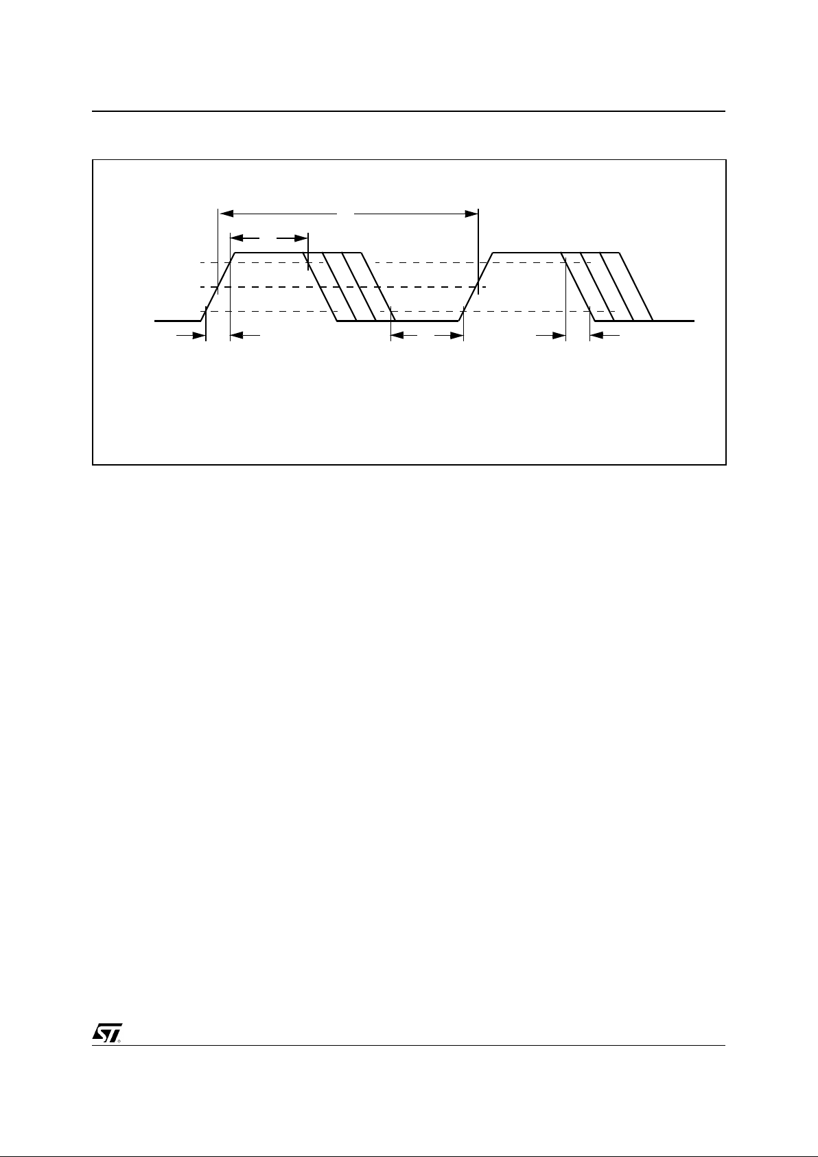
Figure 4-2. CLK Timing Measurement Points
CLK
T5 T4T3
V
Ref
V
IL (MAX)
V
IH (MIN)
T2
T1
LEGEND:
T1 - One Clock Cycle
T2 - Minimum Time at V
IH
T3 - Minimum Time at V
IL
T4 - Clock Fall Time
T5 - Clock Rise Time
NOTE; All sIgnals are sampled on the rising edge of the CLK.
Page 38
ELECTRICAL SPECIFICATIONS
38/87
Release 1.3 - Januar
y
29, 2002
This is preliminary information on a new product now in development or undergoing evaluation. Details are subject to change without notice.
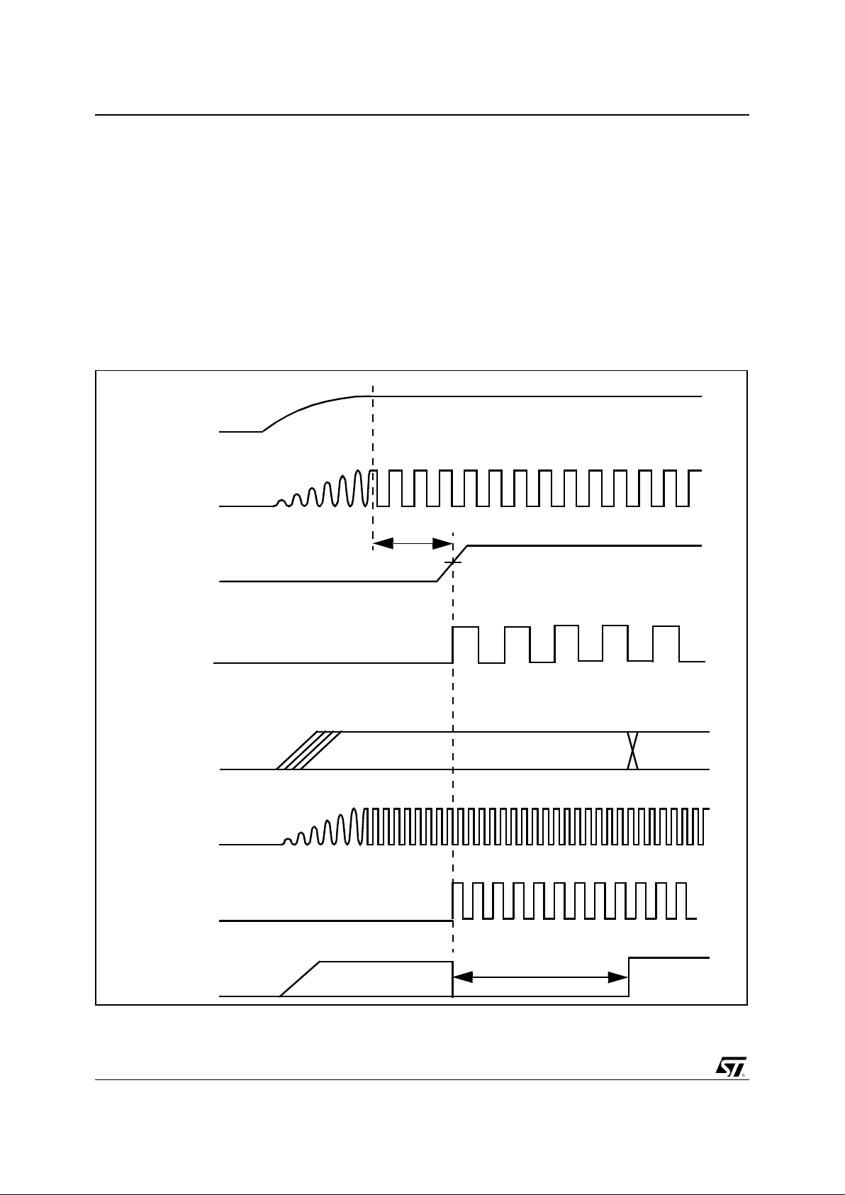
4.5.1. POWER ON SEQUENCE
Figure 4-3 describes the power-on sequence of
the STPC, also called cold reset.
There is no dependency between the different
power supplies and there is no constraint on their
rising time.
SYSRSTI# as no cons traint on its rising e dge but
must stay active until power supplies are all within
specifications, a margin of 10µs is even
recommended to let the STPC PLLs and strap
options stabilize.
Strap Options are continuously sampled during
SYSRSTI# low and must remain stable. Once
SYSRSTI# is high, they MUST NOT CHANGE
until SYSRSTO# goes high.
Bus activity starts only few clock cycles after the
release of SYSRSTO#. The toggling signals
depend on the STPC configuration.
In ISA mode, activity is visible on PCI prior to the
ISA bus as the controller is part of the south
bridge.
In Local Bus mode, the PCI bus is not accessed
and the Flash Chip Select is the control sig nal to
monito r.
Figure 4-3 . Power-on timing di agram
Strap Options
Power Supplies
SYSRSTI#
SYSRSTO#
14 MH z
1.6 V
VALID CONFIGURATION
> 10 us
HCLK
PCI_CLK
2.3 ms
ISACLK
Page 39

ELECTRICAL S PECIFICATIONS
Release 1.3 - January 29, 2002 39/87
This is preliminary information on a new product now in development or undergoing evaluation. Details are subject to change without notice.
4.5.2 RESET SEQUENCE
Figure 4-4 describes the reset sequence of the
STPC, also called warm reset.
The constraints on the strap options and the bus
activities are the same as for the cold reset.
The SYSRSTI# pulse duration must be long
enough to have all the strap options stabilized and
must be adjusted depending on resistor values.
It is mandatory to have a clean reset pulse without
glitches as the STPC could then sample invalid
strap option setting and enter into an umpredictable mode.
While SYSRSTI# is active, the PCI clock P LL runs
in open loop mode at a speed of few 100’s KHz.
Fi
g
ure 4-4. Reset timing diagram
Strap Options
SYSRSTI#
SYSRSTO#
14 M Hz
VALID CONFIGURATION
HCLK
PCI_CLK
2.3 ms
ISACLK
1.6 V
MD[63:0]
Page 40
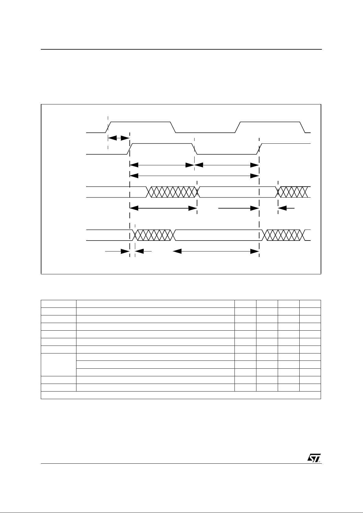
ELECTRICAL SPECIFICATIONS
40/87
Release 1.3 - Januar
y
29, 2002
This is preliminary information on a new product now in development or undergoing evaluation. Details are subject to change without notice.
4.5.3. SDRAM INTERFACE
Figure 4-5 and Table 4-8 list the AC characteris-
tics of the SDRAM interface. The MCLKx clocks
are the input clock of the SDRAM devices
The PC133 memory is recommended to reach
100MHz operation.
Figure 4-5. SDRAM Timing Diagram
MCLKI
STPC.output
STPC.input
MCLKx
T
delay
T
setup
T
hold
T
output (mi n)
T
output (max)
T
cycle
T
high
T
low
Table 4-8. SDRAM Bus AC Timing
Name Parameter Min Typ
Max Unit
Tcycle MCLKI Cycle Time 10 ns
Thigh MCLKI High Time 4 ns
Tlow MCLKI Low Time 4 ns
MCLKI Rising Time 1 ns
MCLKI Falling Time 1 ns
Tdela
y
MCLKx to MCLKI dela
y
-2 ns
Toutput
MCLKI to Outputs Valid
5.2 8.7 ns
MCLKI to DQM[ ] Outputs Valid
4.7 10.9 ns
MCLKI to MD[ ] Outputs Valid
5.1 10.9 ns
Tsetup MD[63:0] setup to MCKLI without RDCLK
0.8 1.8 ns
Thold MD[63:0] hold from MCKLI without RDCLK
0.8 1.6 ns
Note: These timing are for a load of 50pF.
Page 41
ELECTRICAL S PECIFICATIONS
Release 1.3 - January 29, 2002 41/87
This is preliminary information on a new product now in development or undergoing evaluation. Details are subject to change without notice.
4.5.4. PCI INTERFACE
Table 4-9 lists the AC characteristics of the PCI in-
terface.
Table 4-9. PCI Bus AC Timing
Name Parameter
Min Max Unit
PCI_CLKI to AD[31:0] valid - 9.3 ns
PCI_CLKI to FRAME
valid - 7.14 ns
PCI_CLKI to CBE
[3:0] valid - 7.94 ns
PCI_CLKI to PAR valid - 9.34 ns
PCI_CLKI to TRDY
valid - 8.8 ns
PCI_CLKI to IRDY
valid - 7 .74 ns
PCI_CLKI to STOP
valid - 9.4 ns
PCI_CLKI to DEVSEL
valid - 8.5 ns
PCI_CLKI to PCI_GNT
valid - 7.14 ns
AD[31:0] bus setup to PCI_CLKI 5.42 ns
FRAME
setup to PCI_CLKI 5.03 ns
CBE
[3:0] setup to PCI_CLKI 6.37 ns
IRDY
setup to PCI_CLKI 4.52 ns
PCI_REQ
[2:0] setup to PCI_CLKI 5.29 ns
AD[31:0] bus hold from PCI_CLKI -0.91 ns
FRAME
hold from PCI_CLKI -1.8 ns
CBE
[3:0] hold to PCI_CLKI -2.9 ns
IRDY
hold to PCI_CLKI -1.6 ns
PCI_REQ
[2:0] hold from PCI_CLKI -3.49 ns
Page 42

ELECTRICAL SPECIFICATIONS
42/87
Release 1.3 - Januar
y
29, 2002
This is preliminary information on a new product now in development or undergoing evaluation. Details are subject to change without notice.
4.5.5 IPC INTERFACE
Table 4-10 lists the AC characteristics of the IPC
interface.
Figure 4-6. IPC timing diagram
ISACLK
IRQ_MUX[3:0]
DREQ_MUX[1:0]
ISACLK2X
T
dly
T
setup
T
setup
Table 4-10. IPC Interface AC Timings
Name Parameter Min M ax Unit
T
dly
ISACLK2X to ISACLK delay nS
ISACLK2X to DACK_ENC[2:0] valid nS
ISACLK2X to TC valid nS
T
setup
IRQ_MUX[3:0] Input setup to ISACLK2X 0 - nS
T
setup
DREQ_MUX[1:0] Input setup to ISACLK2X 0 - nS
Page 43
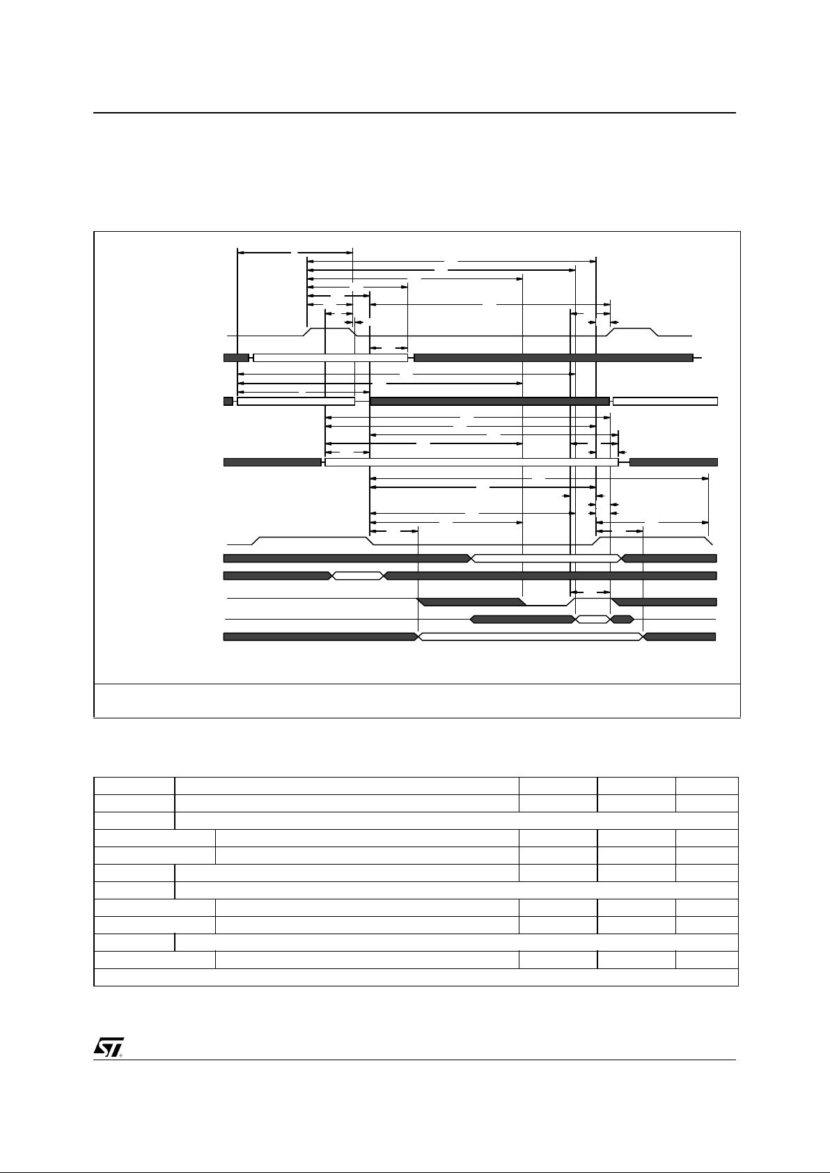
ELECTRICAL S PECIFICATIONS
Release 1.3 - January 29, 2002 43/87
This is preliminary information on a new product now in development or undergoing evaluation. Details are subject to change without notice.
4.5.6 ISA INTERFACE AC TIMING CHARACTERISTICS
Table 4-7 and Table 4-11 l ist the AC characteris-
tics of the ISA interface.
Figure 4-7 ISA Cycle (ref
Table 4-11
)
Note 1: Stands for SMEMR#, SMEMW#, MEMR#, MEMW#, IOR# & IOW#.
The clock has not been represented as it is dependent on the ISA Slave mode.
Valid AENx
Valid Address
Valid Address, SBHE*
V.Dat
a
VALID DATA
54
28
26
64
59
58
55
28
23
61
48
47
26
23
57
27
24
42
41
10
11
34
33
3
22
56
29
25
9
18
2
12
38
37
15
14
13
12
ALE
AEN
LA [23:17]
SA [19:0]
CONTROL (Note 1)
IOCS16#
MCS16#
IOCHRDY
READ DATA
WRITE DATA
Table 4-11. ISA Bus AC Timing
Name Parameter Min Max Units
2 LA[23:17] valid before ALE# negated 5T Cycles
3 LA[23:17] valid before MEMR#, MEMW# asserted
3a Memory access to 16-bit ISA Slave 5T Cycles
3b Memory access to 8-bit ISA Slave 5T Cycles
9 SA[19:0] & SBHE valid before ALE# negated 1T Cycles
10 SA[19:0] & SBHE valid before MEMR#, MEMW# asserted
10a Memory access to 16-bit ISA Slave 2T Cycles
10b Memory access to 8-bit ISA Slave 2T Cycles
10 SA[19:0] & SHBE valid before SMEMR#, SMEMW# asserted
10c Memory access to 16-bit ISA Slave 2T Cycle
Note: The signal numbering refers to
Table 4-7
Page 44

ELECTRICAL SPECIFICATIONS
44/87
Release 1.3 - Januar
y
29, 2002
This is preliminary information on a new product now in development or undergoing evaluation. Details are subject to change without notice.
10d Memory access to 8-bit ISA Slave 2T Cycle
10e SA[19:0] & SBHE valid before IOR#, IOW# asserted 2T Cycles
11 ISACLK2X to IOW# valid
11a Memory access to 16-bit ISA Slave - 2BCLK 2T Cycles
11b Memory access to 16-bit ISA Slave - Standard 3BCLK 2T Cycles
11c Memory access to 16-bit ISA Slave - 4BCLK 2T Cycles
11d Memory access to 8-bit ISA Slave - 2BCLK 2T Cycles
11e Memory access to 8-bit ISA Slave - Standard 3BCLK 2T Cycles
12 ALE# asserted before ALE# negated 1T Cycles
13 ALE# asserted before MEMR#, MEMW# asserted
13a Memory Access to 16-bit ISA Slave 2T Cycles
13b Memory Access to 8-bit ISA Slave 2T Cycles
13 ALE# asserted before SMEMR#, SMEMW# asserted
13c Memory Access to 16-bit ISA Slave 2T Cycles
13d Memory Access to 8-bit ISA Slave 2T Cycles
13e ALE# asserted before IOR#, IOW# asserted 2T Cycles
14 ALE# asserted before AL[23:17]
14a Non comp resse d 15T Cycles
14b Com pressed 15T Cycles
15 ALE# asserted before MEMR#, MEMW#, SMEMR#, SMEMW# negated
15a Memory Access to 16-bit ISA Slave- 4 BCLK 11T Cycles
15e Memory Access to 8-bit ISA Slave- Standard Cycle 11T Cycles
18a ALE# negated before LA[23:17] invalid (non compressed) 14T Cycles
18a ALE# negated before LA[23:17] invalid (compressed) 14T Cycles
22 MEMR#, MEMW# asserted before LA[23:17]
22a Memory access to 16-bit ISA Slave. 13T Cycles
22b Memory access to 8-bit ISA Slave. 13T Cycles
23 MEMR#, MEMW# asserted before MEMR#, MEMW# negated
23b Memory access to 16-bit ISA Slave Standard cycle 9T Cycles
23e Memory access to 8-bit ISA Slave Standard cycle 9T Cycles
23 SMEMR#, SMEMW# asserted before SMEMR#, SMEMW# negated
23h Memory access to 16-bit ISA Slave Standard cycle 9T Cycles
23l Memory access to 16-bit ISA Slave Standard cycle 9T Cycles
23 IOR#, IOW# asserted before IOR#, IOW# negated
23o Memory access to 16-bit ISA Slave Standard cycle 9T Cycles
23r Memory access to 8-bit ISA Slave Standard cycle 9T Cycles
24 MEMR#, MEMW# asserted before SA[19:0]
24b Memory access to 16-bit ISA Slave Standard cycle 10T Cycles
24d Memory access to 8-bit ISA Slave - 3BLCK 10T Cycles
24e Memory access to 8-bit ISA Slave Standard cycle 10T Cycles
24f Memory access to 8-bit ISA Slave - 7BCLK 10T Cycles
24 SMEMR#, SMEMW# asserted before SA[19:0]
24h Memory access to 16-bit ISA Slave Standard cycle 10T Cycles
24i Memory access to 16-bit ISA Slave - 4BCLK 10T Cycles
24k Memory access to 8-bit ISA Slave - 3BCLK 10T Cycles
24l Memory access to 8-bit ISA Slave Standard cycle 10T Cycles
Table 4-11. ISA Bus AC Timing
Name Parameter Min Max Units
Note: The si
g
nal numbering refers to
Table 4-7
Page 45

ELECTRICAL S PECIFICATIONS
Release 1.3 - January 29, 2002 45/87
This is preliminary information on a new product now in development or undergoing evaluation. Details are subject to change without notice.
24 IOR#, IOW# asserted before SA[19:0]
24o I/O access to 16-bit ISA Slave Standard cycle 19T Cycles
24r I/O access to 16-bit ISA Slave Standard cycle 19T Cycles
25 MEMR#, MEMW# asserted before next ALE# asserted
25b Memory access to 16-bit ISA Slave Standard cycle 10T Cycles
25d Memory access to 8-bit ISA Slave Standard cycle 10T Cycles
25 SMEMR#, SMEMW# asserted before next ALE# asserted
25e Memory access to 16-bit ISA Slave - 2BCLK 10T Cycles
25f Memory access to 16-bit ISA Slave Standard cycle 10T Cycles
25h Memory access to 8-bit ISA Slave Standard cycle 10T Cycles
25 IOR#, IOW# asserted before next ALE# asserted
25i I/O access to 16-bit ISA Slave Standard cycle 10T Cycles
25k I/O access to 16-bit ISA Slave Standard cycle 10T Cycles
26 MEMR#, MEMW# asserted before next MEMR#, MEMW# asserted
26b Memory access to 16-bit ISA Slave Standard cycle 12T Cycles
26d Memory access to 8-bit ISA Slave Standard cycle 12T Cycles
26 SMEMR#, SMEMW# asserted before next SMEMR#, SMEMW# asserted
26f Memory access to 16-bit ISA Slave Standard cycle 12T Cycles
26h Memory access to 8-bit ISA Slave Standard cycle 12T Cycles
26 IOR#, IOW# asserted before next IOR#, IOW# asserted
26i I/O access to 16-bit ISA Slave Standard cycle 12T Cycles
26k I/O access to 8-bit ISA Slave Standard cycle 12T Cycles
28 Any command negated to MEMR#, SMEMR#, MEMR#, SMEMW# asserted
28a Memory access to 16-bit ISA Slave 3T Cycles
28b Memory access to 8-bit ISA Slave 3T Cycles
28 Any command negated to IOR#, IOW# asserted
28c I/O access to ISA Slave 3T Cycles
29a MEMR#, MEMW# negated before next ALE# asserted 1T Cycles
29b SMEMR#, SMEMW# negated before next ALE# asserted 1T Cycles
29c IOR#, IOW# negated before next ALE# asserted 1T Cycles
33 LA[23:17] valid to IOCHRDY negated
33a Memory access to 16-bit ISA Slave - 4 BCLK 8T Cycles
33b Memory access to 8-bit ISA Slave - 7 BCLK 14T Cycles
34 LA [23:1 7] valid to read data valid
34b Memory access to 16-bit ISA Slave Standard cycle 8T Cycles
34e Memory access to 8-bit ISA Slave Standard cycle 14T Cycles
37 ALE# asserted to IOCHRDY# negated
37a Memory access to 16-bit ISA Slave - 4 BCLK 6T Cycles
37b Memory access to 8-bit ISA Slave - 7 BCLK 12T Cycles
37c I/O access to 16-bit ISA Slave - 4 BCLK 6T Cycles
37d I/O access to 8-bit ISA Slave - 7 BCLK 12T Cycles
38 ALE# asserted to read data valid
38b Memory access to 16-bit ISA Slave Standard Cycle 4T Cycles
38e Memory access to 8-bit ISA Slave Standard Cycle 10T Cycles
38h I/O access to 16-bit ISA Slave Standard Cycle 4T Cycles
38l I/O access to 8-bit ISA Slave Standard Cycle 10T Cycles
Table 4-11. ISA Bus AC Timing
Name Parameter Min Max Units
Note: The signal numbering refers to
Table 4-7
Page 46

ELECTRICAL SPECIFICATIONS
46/87
Release 1.3 - Januar
y
29, 2002
This is preliminary information on a new product now in development or undergoing evaluation. Details are subject to change without notice.
41 SA[19:0] SBHE valid to IOCHRDY negated
41a Memory access to 16-bit ISA Slave 6T Cycles
41b Memory access to 8-bit ISA Slave 12T Cycles
41c I/O access to 16-bit ISA Slave 6T Cycles
41d I/O access to 8-bit ISA Slave 12T Cycles
42 SA[19:0] SBHE valid to read data valid
42b Memory access to 16-bit ISA Slave Standard cycle 4T Cycles
42e Memory access to 8-bit ISA Slave Standard cycle 10T Cycles
42h I/O access to 16-bit ISA Slave Standard cycle 4T Cycles
42l I/O access to 8-bit ISA Slave Standard cycle 10T Cycles
47 MEMR#, MEMW#, SMEMR#, SMEMW#, IOR#, IOW# asserted to IOCHRDY negated
47a Memory access to 16-bit ISA Slave 2T Cycles
47b Memory access to 8-bit ISA Slave 5T Cycles
47c I/O access to 16-bit ISA Slave 2T Cycles
47d I/O access to 8-bit ISA Slave 5T Cycles
48 MEMR#, SMEMR#, IOR# asserted to read data valid
48b Memory access to 16-bit ISA Slave Standard Cycle 2T Cycles
48e Memory access to 8-bit ISA Slave Standard Cycle 5T Cycles
48h I/O access to 16-bit ISA Slave Standard Cycle 2T Cycles
48l I/O access to 8-bit ISA Slave Standard Cycle 5T Cycles
54 IOCHRDY asserted to read data valid
54a Memory access to 16-bit ISA Slave 1T(R)/2T(W) Cycles
54b Memory access to 8-bit ISA Slave 1T(R)/2T(W) Cycles
54c I/O access to 16-bit ISA Slave 1T(R)/2T(W) Cycles
54d I/O access to 8-bit ISA Slave 1T(R)/2T(W) Cycles
55a
IOCHRDY asserted to MEMR#, MEMW#, SMEMR#, SMEMW#,
IOR#, IOW# negated
1T Cycles
55b IOCHRY asserted to MEMR#, SMEMR# negated (refresh) 1T Cycles
56 IOCHRDY asserted to next ALE# asserted 2T Cycles
57 IOCHRDY asserted to SA[19:0], SBHE invalid 2T Cycles
58 MEMR#, IOR#, SMEMR# negated to read data invalid 0T Cycles
59 MEMR#, IOR#, SMEMR# negated to data bus float 0T Cycles
61 Write data before MEMW# asserted
61a Memory access to 16-bit ISA Slave 2T Cycles
61b
Memory access to 8-bit ISA Slave (Byte copy at end of
start)
2T Cycles
61 Write data before SMEMW# asserted
61c Memory access to 16-bit ISA Slave 2T Cycles
61d Memory access to 8-bit ISA Slave 2T Cycles
61 Write Data valid before IOW# asserted
61e I/O access to 16-bit ISA Slave 2T Cycles
61f I/O access to 8-bit ISA Slave 2T Cycles
64a MEMW# negated to write data invalid - 16-bit 1T Cycles
64b MEMW# negated to write data invalid - 8-bit 1T Cycles
64c SMEMW# negated to write data invalid - 16-bit 1T Cycles
64d SMEMW# negated to write data invalid - 8-bit 1T Cycles
Table 4-11. ISA Bus AC Timing
Name Parameter Min Max Units
Note: The si
g
nal numbering refers to
Table 4-7
Page 47

ELECTRICAL S PECIFICATIONS
Release 1.3 - January 29, 2002 47/87
This is preliminary information on a new product now in development or undergoing evaluation. Details are subject to change without notice.
64e IOW# negated to write data invalid 1T Cycles
64f
MEMW# negated to copy data float, 8-bit ISA Slave, odd Byte
by ISA Master
1T Cycles
64g
IOW# negated to copy data float, 8-bit ISA Slave, odd Byte by
ISA Master
1T Cycles
Table 4-11. ISA Bus AC Timing
Name Parameter Min Max Units
Note: The signal numbering refers to
Table 4-7
Page 48

ELECTRICAL SPECIFICATIONS
48/87
Release 1.3 - Januar
y
29, 2002
This is preliminary information on a new product now in development or undergoing evaluation. Details are subject to change without notice.
4.5.7 LOCAL BUS INTERFACE
Figure 4-3 to Figure 4-11 and Table 4-13 li st the
AC characteristics of the Local Bus interface.
Figure 4-8. Synchronous Read Cycle
PA[ ] bus
CSx#
PRD#[1:0]
PD[15:0]
HCLK
T
setup
T
active
T
hold
Figure 4-9. Asynchronous Read Cycle
PA[ ] bus
CSx#
PRD#[1:0]
PD[15:0]
HCLK
T
setup
T
end
T
hold
PRDY
Page 49

ELECTRICAL S PECIFICATIONS
Release 1.3 - January 29, 2002 49/87
This is preliminary information on a new product now in development or undergoing evaluation. Details are subject to change without notice.
Figure 4-1 0. S ynchronous Wri t e Cy c le
PA[ ] bus
CSx#
PWR#[1:0]
PD[15:0]
HCLK
T
setup
T
active
T
hold
Figure 4-11. Asynchronous Write Cycle
PA[ ] bus
CSx#
PWR#[1:0]
PD[15:0]
HCLK
T
setup
T
end
T
hold
PRDY
Page 50
ELECTRICAL SPECIFICATIONS
50/87
Release 1.3 - Januar
y
29, 2002
This is preliminary information on a new product now in development or undergoing evaluation. Details are subject to change without notice.
The Table 4-12 below refers to Vh, Va, Vs which
are the register value for Setup time, A ctive Time
and Hold time, as described in the P rogramming
Manual.
Table 4-12. Local Bus cycle lenght
Cycle T
setup
T
active
T
hold
T
end
Unit
Memory (FCSx#) 4 + Vh 2 + Va 4 + Vs 4 HCLK
Peripheral (IOCSx#) 8 + Vh 3 + Va 4 + Vs 4 HCLK
Table 4-13. Local Bus Interface AC Timing
Name Parameters Min Max Unit s
HCLK to PA bus - 15 nS
HCLK to PD bus - 15 nS
HCLK to FCS#[1:0] - 15 nS
HCLK to IOCS#[3:0] - 15 nS
HCLK to PWR#[1:0] - 15 nS
HCLK to PRD#[1:0] - 15 nS
PD[15:0] Input setup to HCLK - 4 nS
PD[15:0] Input hold to HCLK 2 - nS
PRDY Input setup to HCLK - 4 nS
PRDY Input hold to HCLK 2 - nS
Page 51

ELECTRICAL S PECIFICATIONS
Release 1.3 - January 29, 2002 51/87
This is preliminary information on a new product now in development or undergoing evaluation. Details are subject to change without notice.
4.5.8. IDE INTERFACE
Table 4-14 lists the AC characteristics of the IDE
interface.
Table 4-14. IDE Interface Timing
Name Parameters Min Max Units
DD[15:0] setup to PIOR#/SIOR# falling 15 - ns
DD[15:0} hold to PIOR#/SIOR# falling 0 - ns
Page 52

ELECTRICAL SPECIFICATIONS
52/87
Release 1.3 - Januar
y
29, 2002
This is preliminary information on a new product now in development or undergoing evaluation. Details are subject to change without notice.
4.5.9 JTAG INTERFACE
Figure 4-12 and Table 4-15 list the AC
characteristics of the JTAG interface.
Figure 4-12. JTAG timing diagram
Table 4-15. JTAG AC Timings
Name Parameter Min Max Unit
Treset TRST pulse width 1 Tcycle
Tcycle TCLK period 400 ns
TCLK rising time 20 ns
TCLK falling time 20 ns
Tjset TMS setup time 200 ns
Tjhld TMS hold time 200 ns
Tjset TDI setup time 200 ns
Tjhld TDI hold time 200 ns
Tjout TCLK to TDO valid 30 ns
Tpset STPC pin setup time 30 ns
Tphld STPC pin hold time 30 ns
Tpout TCLK to STPC pin valid 30 ns
TCK
STPC.input
TRST
T
reset
T
cycle
STPC.output
TMS,TDI
TDO
T
jset
T
jhld
T
jout
T
psetTphld
T
pout
Page 53
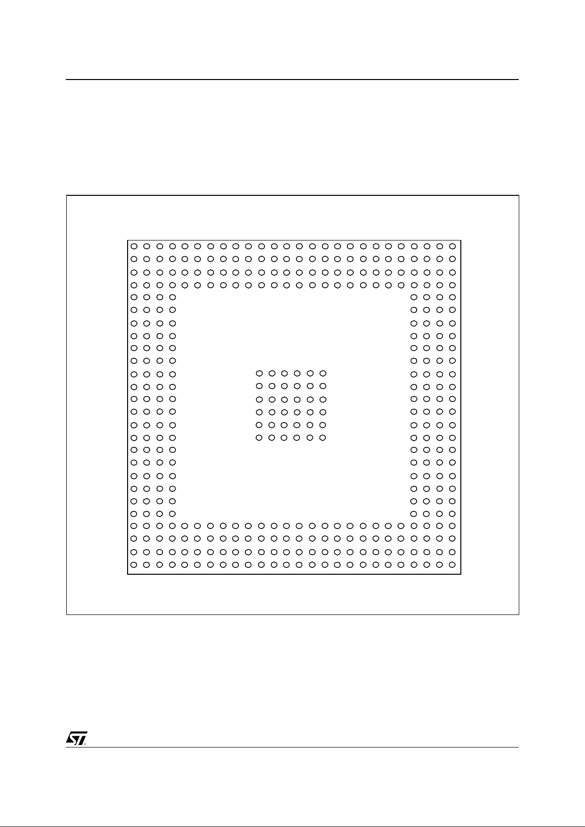
MECHANICAL DATA
Release 1.3 - January 29, 2002 53/87
5. MECHAN ICAL DATA
5.1. 388-PIN PACKAGE DIMENSION
The pin numbering for the ST PC 388-pin Plastic
BGA package is shown in Figure 5-1.
Dimensions are shown in Figure 5-2, Table 5-1
and Figure 5-3, Table 5-2.
Figure 5-1. 388-Pin PBGA Package - Top View
A
B
D
E
F
G
H
J
K
L
M
N
P
R
T
U
V
W
Y
AA
AB
AC
AD
AE
AF
C
135791113151719212325
2 4 6 8 10 12 14 16 18 20 22 24 26
A
B
D
E
F
G
H
J
K
L
M
N
P
R
T
U
V
W
Y
AA
AB
AC
AD
AE
AF
C
135791113151719212325
2468101214161820222426
Page 54
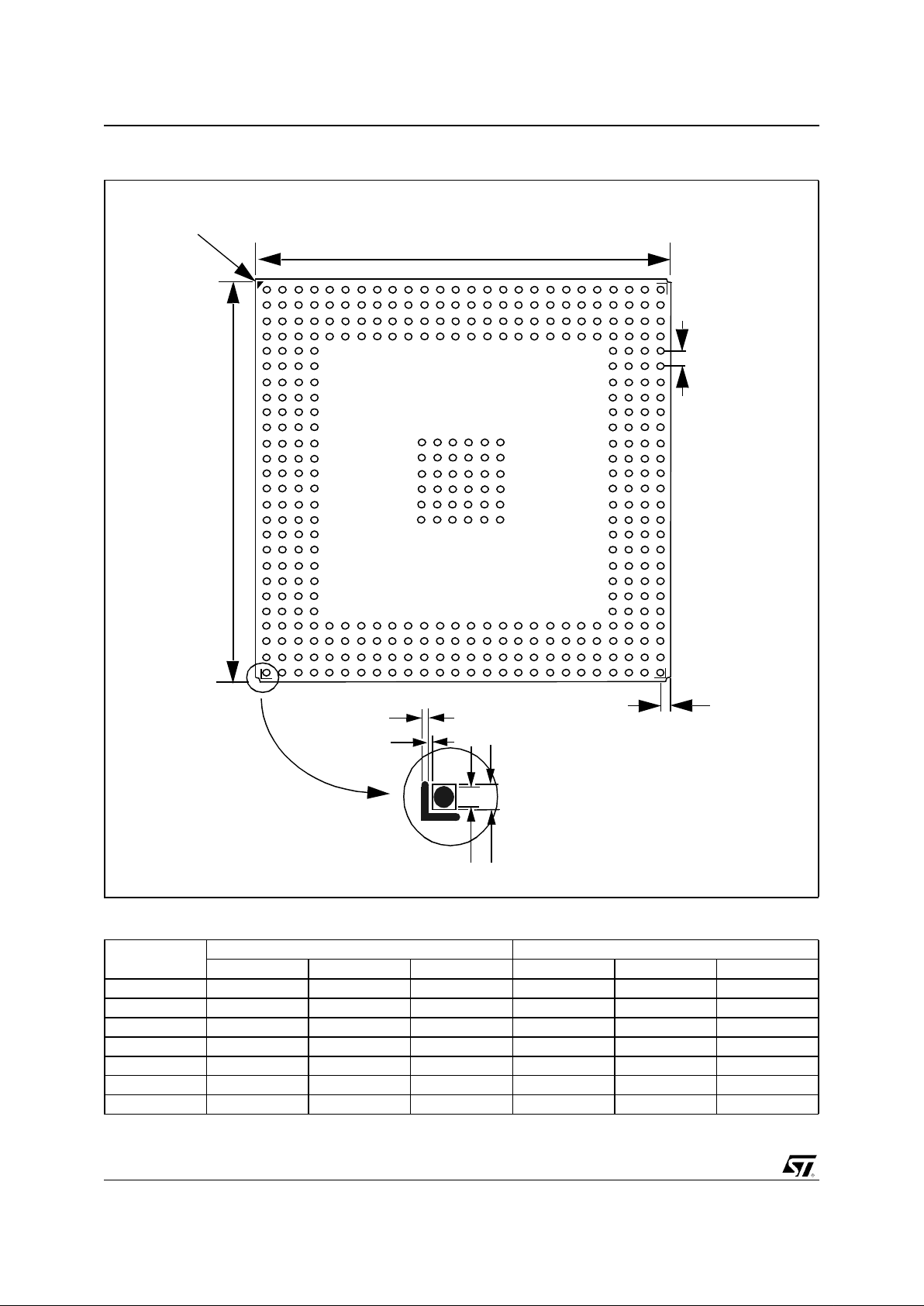
MECHANICAL DATA
54/87
Release 1.3 - Januar
y
29, 2002
Figure 5-2. 388-pin PBGA Package - PCB Dimensions
Table 5-1. 388-pin PBGA Package - PCB Dimensions
Symbols
mm inches
Min Typ Max Min Typ Max
A 34.95 35.00 35.05 1.375 1.378 1.380
B 1.22 1.27 1.32 0.0 48 0.050 0.052
C 0.58 0.63 0.6 8 0.023 0.025 0.027
D 1.57 1.62 1.6 7 0.062 0.064 0.066
E 0.15 0.20 0.25 0.0 06 0.008 0.001
F 0.05 0.10 0.15 0.002 0.004 0.006
G 0.75 0.80 0.85 0.030 0.032 0.034
A
A
B
Detail
A1 Ball Pad Corner
D
F
E
G
C
Page 55

MECHANICAL DATA
Release 1.3 - January 29, 2002 55/87
Figure 5-3. 388-pin PBGA Package - Dimensions
Table 5-2. 388-pin PBGA Package - Dimensions
Symbols
mm inches
Min Typ Max Min Typ Max
A 0.50 0.56 0.62 0.0 20 0.022 0.024
B 1.12 1.17 1.22 0.0 44 0.046 0.048
C 0.60 0.76 0.9 2 0.024 0.030 0.036
D 0.52 0.53 0.5 4 0.020 0.021 0.022
E 0.63 0.78 0.93 0.0 25 0.031 0.037
F 0.60 0.63 0.66 0.024 0.025 0.026
G 30.0 11.8
A
B
C
Solderball
Solderball after collapse
D
E
F
G
Page 56
MECHANICAL DATA
56/87
Release 1.3 - Januar
y
29, 2002
5.2. 388-PIN PACKAGE THERMAL DATA
The 388-pin PBGA package has a Power
Dissipation Capab ility of 4.5W . This increas es to
6W when used with a Heatsink.
The structure in shown in Fi
g
ure 5-4.
Thermal dissipation options are illustrated in
Fi
g
ure 5-5 and Figure 5-6.
Figure 5-4. 388-Pin PBGA structure
Thermal balls
Power & Ground layersSignal layers
Figure 5-5. Thermal Dissipation Without Heatsink
Ambient
Board
Case
Junction
Board
Ambient
Ambient
Case
Junction
Board
Rca
Rjc
Rjb
Rba
66
1258.5
Rja = 13 °C/W
Airflow = 0
Board dimensions:
The PBGA is centred on board
Copper thickness:
- 17µm for internal layers
- 34µm for external layers
- 10.2 cm x 12.7 cm
- 4 layers (2 for signals, 1 GND, 1VCC)
There are no other devices
1 via pad per ground ball (8-mil wire)
40% copper on signal layers
Board temperature taken at the centrecentre b
a
Page 57

MECHANICAL DATA
Release 1.3 - January 29, 2002 57/87
Figure 5-6. Thermal Dissipation With Heatsink
Board
Ambient
Case
Junction
Board
Ambient
Ambient
Case
Junction
Board
Rca
Rjc
Rjb
Rba
36
508.5
Rja = 9.5 °C/W
Airflow = 0
Board dimensions:
The PBGA is centred on board
Copper thickness:
- 17µm for internal layers
- 34µm for external layers
- 10.2 cm x 12.7 cm
- 4 layers (2 for signals, 1 GND, 1VCC)
There are no other devices
Heat sink is 11.1°C/W
1 via pad per ground ball (8-mil wire)
40% copper on signal layers
Board temperature taken at the centre balls
Page 58

MECHANICAL DATA
58/87
Release 1.3 - Januar
y
29, 2002
5.3. SOLDERING RECOMMENDATIONS
High quality, low defect soldering requires
identifying the
optimum temperature profile
for
reflowing the solder paste, therefore optimizing
the process. The heating and cooling rise rates
must be compatible with the solder paste and
components. A typical profile consists of a
preheat, dryout, reflow and cooling sections.
The most critical parameter in the
preheat
section
is to minimize the rate of temperature rise
to less than 2°C / second, in order to minimize
thermal shock on the semi-conductor
components.
Dryout section
is used primarily to ensure that
the solder paste is fully dried b efore hitting reflow
temperatures.
Solder reflow is accomplished in the
reflow zone
,
where the solder paste is elevated to a
temperature greater than the melting point of the
solder. Melting temperature must be exceeded by
approximately 20°C to ensure quality reflow.
In reality the profile is not a line, but rather
a range
of temperatures
all solder joints must be
exposed. The total temperature deviation from
component thermal mism atch, oven loading and
oven uniformity must be within the band.
Figure 5-7. Reflow soldering temperature rang e
Temperature ( °C )
Time ( s )
PREHEAT DRYOUT REFLOW COOLING
240
0
250
200
150
100
50
0
Page 59
DESIGN GUIDELINES
Release 1.3 - January 29, 2002 59/87
This is preliminary information on a new product now in development or undergoing evaluation. Details are subject to change without notice.
6. DESIGN GUIDELINES
6.1. TYPICAL APPLICATIONS
The STPC Elite is well suited for many displayless applications or together with a PCI graphics/
video device. Some of the possible
implementations are described below.
6.1.1. FILE SERVER
A file server is LAN hot-pluggable system that
enables the user to obtain additionnal disk
capacity with great flexibility.
Figure 6-1. File server
STPC
ELITE
SDRAM
64
FLASH
LAN
16
PCI
IDE
Page 60

DESIGN GUIDELINES
60/87 Release 1.3 - January 29, 2002
This is preliminary information on a new product now in development or undergoing evaluation. Details are subject to change without notice.
6.2. STPC CONFIGURATION
The STPC is a very flexible product thanks to
decoupled clock domains and to strap options
enabling a user-optimized configuration.
As some trade off are often necessary, it is
important to do an analysis of the application
needs prior to design a system based on this
product. The applicative constraints are usually
the following:
- CPU performance
- graphics / video performances
- power consumption
- PCI bandwidth
- booting time
- EMC
Some other elements can help to tune the choice:
- Code size of CPU Consuming tasks
- Data size and location
On the STPC side, the configurable parameters
are the following:
- synchronous / asynchronous mode
- HCLK speed
- MCLK speed
- CPU clock ratio (x1, x2)
- Local Bus / ISA bus
6.2.1. LOCAL BUS / ISA BUS
The selection b etwe en the ISA bus and the Local
Bus is relatively simple. The first one is a standard
bus but slow. The Local Bus is fast and
programmable but doesn't su pport any DMA nor
external master mechanisms. The Table 6-1
below summarize the selection:
Before implementing a function requiring DMA
capability on the ISA bus, it is recommended to
check if it exists on PCI, or if it can be
implemented differently, in order to use the local
bus mode.
6.2.2. CLOCK CONFIGURATION
The CPU clock and the memory clock are
independent unless the "synchronous mode"
strap option is set (see the STRAP OPTIONS
chapter). The potential clock configurations are
then relatively limited as listed in Table 6-2.
The advantage of the synchronous mode
compared to the asynchronous mode is a lower
latency when accessing SDRAM from the CPU or
the PCI (saves 4 MCLK cycles for the first access
of the burst). For the same CPU to Memory
transfer performance, MCLK as to be roughly
higher by 20MHz between SYNC and ASYNC
modes (example: 66MHz SYNC = 96MHz
ASYNC).
In all cases, use SDRAM with CAS Latency
equals to 2 (CL2) for the best performances.
The advantage of the asynch ronous mode is the
capability to reprogram the MCLK speed on the
fly. This could help for applications were power
consumption must be optimized.
Regarding PCI bandwidth, the best is to have
HCLK at 100MHz as it gives twice the bandwidth
compared to HCLK at 66MHz.
The last, and more complex, information to
consider is the behaviour of the software. In case
high CPU or FPU computation is needed, it is
sometime better to be in DX2-133/MCLK=66
synchronous mode than DX2-133/MCLK=100
asynchronous mode. This depend s on the locality
of the number crunching code and the amount of
data manipulated.
The Table 6-3 below gives some ex amples. The
right column correspond to the configuration
number as described in Table 6-2:
Obviously, the values for HCLK or MCLK can be
reduced compared to Table 6-2 in case there is no
need to push the device at its limits, or when
avoiding to use specific frequency ranges (FM
radio band for example).
Table 6-1.
Bus mode selection
Need Selection
Legacy I/O device (Floppy, ...), Super I/O ISA Bus
DMA capability (Soundblaster) ISA Bus
Flash, SRAM, basic I/O device Local Bus
Fast boot Local Bus
Boot flash of 4MB or more Local Bus
Programmable Chip Select Local Bus
Table 6-2.
Main STPC modes
CMode
HCLK
MHz
CPU clock
clock ratio
MCLK
MHz
1 Synchronous 66 133 (x2) 66
2 Asynchronous 66 133 (x2) 100
3 Synchronous 100 100 (x1) 100
Table 6-3.
Clock mode selection
Constraints C
Need CPU power
Critical code fits into L1 cache
1
Need CPU power
Code or data does not fit into L1 cache
3
Need high PCI bandwitdh 3
Need flexible SDRAM speed 2
Page 61
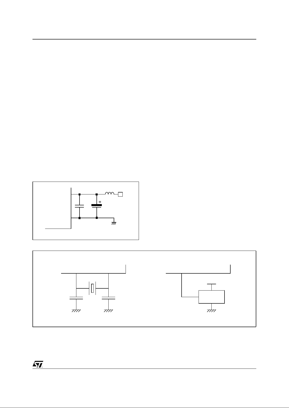
DESIGN GUIDELINES
Release 1.3 - January 29, 2002 61/87
This is preliminary information on a new product now in development or undergoing evaluation. Details are subject to change without notice.
6.3. ARCHITECTURE RECOMMENDATIONS
This section describes the recommend
implementations for the STPC interfaces. For
more details, download the
Reference
Schematics
from the STPC web site.
6.3.1. POWER DECOUPLING
An appropriate decoupling of the various STPC
power pins is mandatory for optimum behaviou r.
When insufficient, the integrity of the signals is
deteriorated, the stability of the system is reduced
and EMC is increased.
6.3.1.1. PLL decoupling
This is the most important as the STPC clocks are
generated from a single 14MHz stage using
multiple PLLs which are highly sensitive analog
cells. The frequenc ies to filter are the 25-50 KHz
range which correspond to the internal loop
bandwidth of the PLL and the 10 to 100 MHz
frequency of the output. PLL power pins can be
tied together to simplify the board layout.
6.3.1.2. Decoupling of 3.3V and Vcore
A power plane for each of these supplies with one
decoupling capacitance for each power pin is the
minimum. The use of multiple capacitances with
values in decade is the bes t (for example: 10pF,
1nF, 100nF, 10uF), the smallest value, the closest
to the power pin. Connecting the various digital
power planes through capacitances will reduce
furthermore the overall impedance and electrical
noise.
6.3.2. 14MHZ OSCILLATOR STAGE
The 14.31818 MHz oscillator stage can be
implemented using a quartz, which is the
preferred and cheaper solution, or using an
external 3.3V oscillator.
The crystal must be used in its series-cut
fundamental mode and n ot in overtone mode. It
must have an Equivalent Series Resistance (ESR,
sometimes referred to as Rm) of less than 50
Ohms (typically 8 Ohms) and a shunt capacitance
(Co) of less than 7 pF. The ba lance capa citors of
16 pF must be added, one connected to each pin,
as described in Figure 6-3.
In the event of an ext ernal o scillat or pr ovidin g the
master clock signal to the STPC Atlas device, the
LVTTL signal should be connected to XTALI, as
described in Figure 6-3.
As this clock is the reference for all the other onchip generated clocks, it is
strongly
recommended to shield this stage
, including
the 2 wires going to the STPC balls, in order to
reduce the jitter to the minimum and reach the
optimum system stability.
Figure 6-2. PLL decoupling
VDD_PLL
VSS_PLL
PWR
100nF 47uF
GND
Connections must be as s hort as possible
Figure 6-3. 14.31818 MHz stage
15pF15pF
XTALOXTALI XTALOXTALI
3.3V
Page 62

DESIGN GUIDELINES
62/87 Release 1.3 - January 29, 2002
This is preliminary information on a new product now in development or undergoing evaluation. Details are subject to change without notice.
6.3.3. SDRAM
The STPC provides all the signals for SDRAM
control. Up to 128 MBytes of main memory are
supported. All Banks must be 64 bits wide. Up to 4
memory banks are available when using 16Mbit
devices. Only up to 2 banks can be connected
when using 64Mbit and 128Mbit c omponents due
to the reallocation of CS2# and CS3# signals. This
is described in Table 6-4 and Table 6-5.
Graphics memory resides at the beginning of
Bank 0. Host memory begins at the top of graphics
memory and extends to the top of populated
SDRAM. Bank 0 must always be populated.
Figure 6-4, Figure 6-5 and Figure 6-6 show some
typical implementations.
The purpose of the serial resistors is to reduce
signal oscillation and EMI by filtering line
reflections. The capacitance in F igure 6-4 has a
filtering effect too, while it is used for propagat ion
delay compensation in the 2 other figures.
Figure 6-4. One Memory Bank with 4 Chips (16-bit)
CS0#
BA[1:0]
MA[12:0]
WE#
RAS0#
DQM[7:0]
MCLKI
MCLKO
DQM[7:6]
Reference Knot
CAS0#
MD[63:48]
DQM[5:4]
MD[47:32]
DQM[3:2]
MD[31:16]
DQM[1:0]
MD[15:0]
MD[63:0]
MCLKA
MCLKBMCLKCMCLKD
10pF
Length(MCLKI) = Length(MCLKy) with y = {A,B,C,D}
Page 63

DESIGN GUIDELINES
Release 1.3 - January 29, 2002 63/87
This is preliminary information on a new product now in development or undergoing evaluation. Details are subject to change without notice.
Figure 6-5. One Memory Banks with 8 Chips (8-bit)
Figure 6-6. Two Memory Banks with 8 Chips (8-bit)
CS0#
BA[1:0]
MA[12:0]
WE#
RAS0#
DQM[7:0]
MCLKI
MCLKO
DQM[7]
CAS0#
MD[63:56]
DQM[0]
MD[7:0]
MD[63:0]
A
10pF Length(MCLKI) = Length(MCLKy) with y = {A,B,C,D,E,F,G,H}
DQM[1]
MD[15:8]
BCDEFG
H
CY2305
CS1#
BA[1:0]
MA[12:0]
WE#
RAS0#
DQM[7:0]
MCLKI
MCLKO
DQM[7]
CAS0#
MD[63:56]
DQM[0]
MD[7:0]
MD[63:0]
A
1
22pF
Length(MCLKI) = Length(MCLKy
x
) with
DQM[1]
MD[15:8]
B
1
C
1
D
1
E
1
F
1
G
1
H
1
CS0#
A
0
B
0
C
0
D
0
E
0
F
0
G
0
H
0
x = {0,1}
y = {A,B,C,D,E,F,G,H}
CY2305
Page 64
DESIGN GUIDELINES
64/87 Release 1.3 - January 29, 2002
This is preliminary information on a new product now in development or undergoing evaluation. Details are subject to change without notice.
For other implementations like 32-bit SDRAM
devices, refers to the SDRAM controller signal
multiplexing and address mapping described in
the following Table 6-4 and Table 6-5.
Tabl e 6-4.
DIMM Pinout
SDRAM Density 16 Mbit 64/128 Mbit 64/128 Mbit
STPC I/F
Internal Banks 2 Banks 2 Banks 4 Banks
DIMM Pin Number
... MA[10:0] MA[10:0] MA[10:0] MA[10:0]
123 - MA11 MA11 CS2# (MA11)
126 - MA12 - CS3# (MA12)
39 - - BA1 (MA12) CS3# (BA1)
122 BA0 (MA11) BA0 (MA13) BA0 (MA13) BA0
Table 6-5.
Address Mapping
Address Mapping: 16 Mbit - 2 internal banks
STPC I/F BA0 MA10 MA9 MA8 MA7 MA6 MA5 MA4 MA3 MA2 MA1 MA0
RAS Address A11 A22 A21 A2 A19 A18 A17 A16 A15 A14 A13 A12
CAS Address A11 0 A24 A23 A10 A9 A8 A7 A6 A5 A4 A3
Address Mapping: 64/128 Mbit - 2 internal banks
STPC I/F BA0 MA12 MA11 MA10 MA9 MA8 MA7 MA6 MA5 MA4 MA3 MA2 MA1 MA0
RAS Address A11 A24 A23 A22 A21 A20 A19 A18 A17 A16 A15 A14 A13 A12
CAS AddressA110 0 0 A26A25A10A9A8A7A6A5A4A3
Address Mapping: 64/128 Mbit - 4 internal banks
STPC I/F BA0 BA1 MA11 MA10 MA9 MA8 MA7 MA6 MA5 MA4 MA3 MA2 MA1 MA0
RAS Address A11 A12 A24 A23 A22 A21 A20 A19 A18 A17 A16 A15 A14 A13
CAS Address A11 A12 0 0 A26 A25 A10 A9 A8 A7 A6 A5 A4 A3
Page 65

DESIGN GUIDELINES
Release 1.3 - January 29, 2002 65/87
This is preliminary information on a new product now in development or undergoing evaluation. Details are subject to change without notice.
6.3.4. PCI BUS
The PCI bus is always active and the following
control signals must be pulled-up to 3.3V or 5V
through 2K2 resistors even if this bus is not
connected to an external device: FRAME#,
TRDY#, IRDY#, STOP#, DEVSEL#, LOCK#,
SERR#, PCI_REQ#[2:0].
PCI_CLKO must be connected to PCI_CLKI
through a 10 to 33 Ohms resistor. Figure 6-7
shows a typical implementation.
For more information on layout constraints, go to
the
place and route recommendations
section.
In the case of higher clock load it is recommended
to use a zero-delay clock buf fer as described in
Figure 6 -8. This approach is also recommended
when implementing the delay on PCICLKI
according to the PCI section of the
Electrical
Specifications
chapter.
Figure 6-7. Typ ic a l PC I cl ock routing
PCICLKI
PCICLKO
PCICLKA
PCICLKB
PCICLKC
0 - 22
10 - 33
Device A
Device B
Device C
0 - 33pF
Figure 6-8. PCI clock routing with zero-delay clock buffer
PCICLKI
PCICLKO
Device A
Device B
Device C
PLL
Device D
PCICLKI
PCICLKO
Device A
Device B
Device C
PLL
Device D
CY2305CY2305
Implementation 1 Implementation 2
Page 66
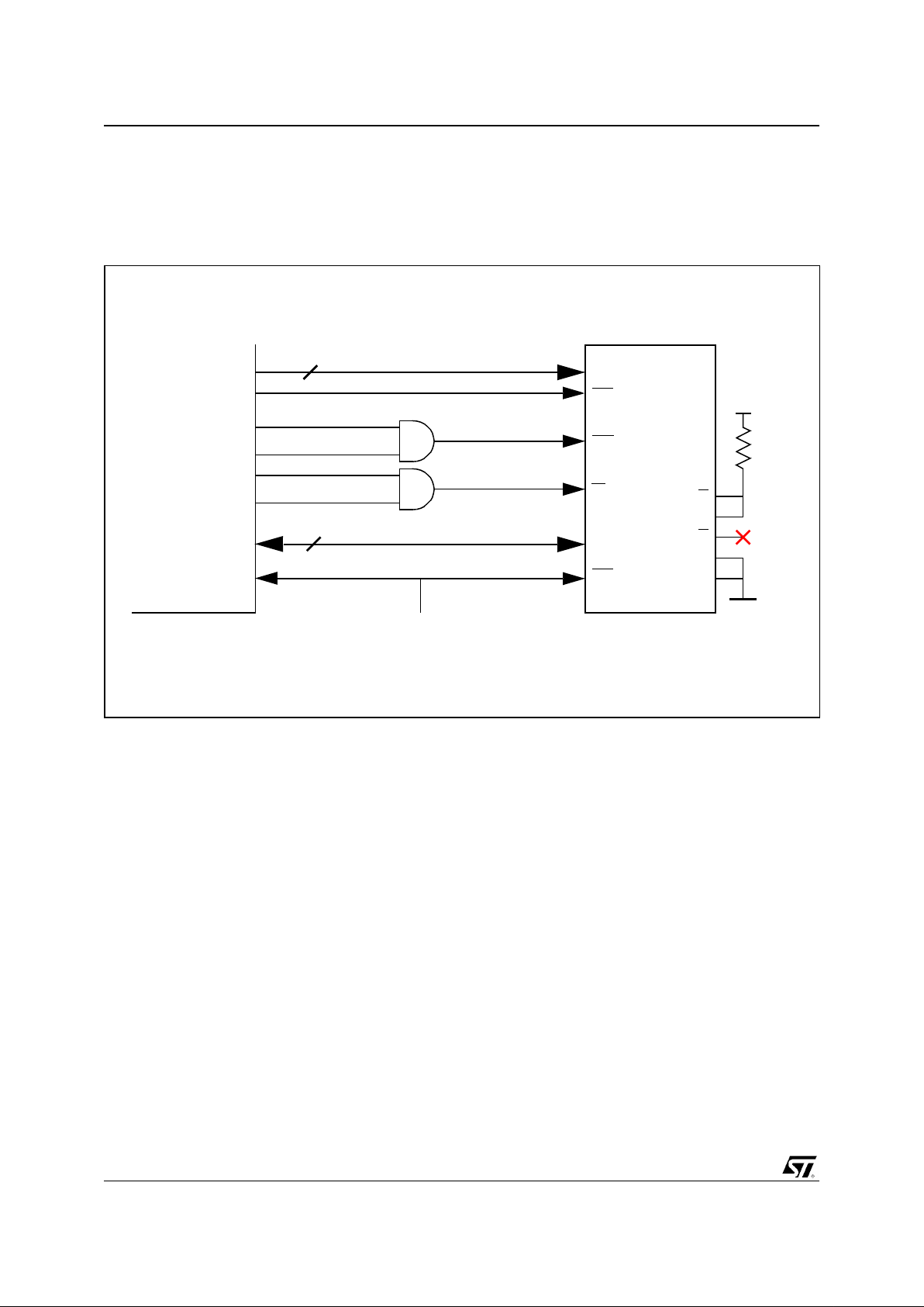
DESIGN GUIDELINES
66/87 Release 1.3 - January 29, 2002
This is preliminary information on a new product now in development or undergoing evaluation. Details are subject to change without notice.
6.3.5. LOCAL BUS
The local bus has all the signals to conn ect flash
devices or I/O devices with the minimum glue
logic.
Figure 6-9 describes how to connect a 16-bit boot
flash (the corresponding strap options must be set
accordingly).
Fi
g
ure 6-9.
Typical 16-bit boot flash implementation
M58LW064A
STPC
22
DQ[15:0]
A[22:1]
CE
OE
W
RP
B
CLK
RB
LE
R
3V3
GND
RESET#
16
PD[15:0]
FCS0#
PWR0#
SYSRSTI#
PRD0#
PA[22:1]
PRD1#
PWR1#
Page 67

DESIGN GUIDELINES
Release 1.3 - January 29, 2002 67/87
This is preliminary information on a new product now in development or undergoing evaluation. Details are subject to change without notice.
6.3.6. IPC
Most of the IPC signals are multiplexed: Interrupt
inputs, DMA Request i nputs, DMA Acknowledge
outputs. The figure below describes a complete
implementation of the IRQ[15:0] time-multiplexing.
When an interrupt line is used internally, the
corresponding input can be grounded. In most of
the embedded des igns, only few interrupts lines
are necessary and the glue logic can be simplified.
When the interface is integrated into the STPC,
the corresponding interrupt line can be groun ded
as it is connected internally.
For example, if the integrated IDE controller is
activated, the IRQ[14] and IRQ[ 15] inputs can be
grounded.
Figure 6-10. Typical IRQ multiplexing
74x153
1C0
1Y
1G
IRQ[0]
IRQ_MUX[0]
1C1
1C2
1C3
2C0
2C1
2C2
2C3
A
B
2G
2Y IRQ_MUX[1]
IRQ[1]
IRQ[2]
IRQ[3]
IRQ[4]
IRQ[5]
IRQ[6]
IRQ[7]
74x153
1C0
1Y
1G
IRQ_MUX[2]
1C1
1C2
1C3
2C0
2C1
2C2
2C3
A
B
2G
2Y IRQ_MUX[3]
IRQ[8]
IRQ[9]
IRQ[10]
IRQ[11]
IRQ[12]
IRQ[13]
IRQ[14]
IRQ[15]
ISA_CLK2X
ISA_CLK
Timer 0
Keyboard
Slave PIC
COM2/COM4
COM1/COM3
LPT2
LPT1
RTC
Mouse
FPU
PCI / IDE
PCI / IDE
Floppy
Floppy
Page 68

DESIGN GUIDELINES
68/87 Release 1.3 - January 29, 2002
This is preliminary information on a new product now in development or undergoing evaluation. Details are subject to change without notice.
The figure below describes a complete
implementation of the external glue logic for DMA
Request time-multiplexing and DMA Acknowledge
demultiplexing. Like for the interrupt lines, this
logic can be simplified when only few DMA
channels are used in the application.
This glue logic is not needed in Local bus mode as
it does not support DMA transfers.
Figure 6-11. Typical DMA multiplexing and demultiplexing
74x153
1C0
1Y
1G
DRQ[0]
DREQ_MUX[0]
1C1
1C2
1C3
2C0
2C1
2C2
2C3
A
B
2G
2Y DREQ_MUX[1]
DRQ[1]
DRQ[2]
DRQ[3]
DRQ[4]
DRQ[5]
DRQ[6]
DRQ[7]
74x138
Y0#
A
G2B
DACK0#
Y1#
Y2#
Y3#
Y4#
Y5#
Y6#
Y7#
C
B
G2A
ISA_CLK2X
ISA_CLK
ISA, Refresh
ISA, PIO
ISA, FDC
ISA, PIO
Slave DMAC
ISA
ISA
ISA
G1
DMA_ENC[0]
DMA_ENC[1]
DMA_ENC[2]
DACK1#
DACK2#
DACK3#
DACK5#
DACK6#
DACK7#
Page 69

DESIGN GUIDELINES
Release 1.3 - January 29, 2002 69/87
This is preliminary information on a new product now in development or undergoing evaluation. Details are subject to change without notice.
6.3.7. IDE / ISA DYNAMIC DEMULTIPLEXING
Some of the ISA bus signals are dynamically
multiplexed to optimize the pin count. Figure 6-12
describes how to implement the external glue
logic to demultiplex the IDE and ISA interfaces. In
Local Bus mode the two buffers are not needed
and the NAND gates can be simplified to inverters.
6.3.8. BASIC AUDIO USING IDE INTERFACE
When the application requires only basic audio
capabilities, an audio DAC on the IDE interface
can avoid using a PCI-based audio device. This
low cost solution is not CPU cons uming t hanks to
the DMA controller implemented in the IDE
controller and can generat e 16-bit stereo sound.
The clock speed is programmable when using the
speaker output.
Figure 6-12. Typical IDE / ISA Demultiplexing
MASTER#
74xx245
RMRTCCS#
A
B
DIR
OE
ISAOE#
KBCS#
RTCRW#
RTCDS
SA[19:8]
STPC bus / DD[15:0]
LA[24]
LA[25]
LA[22]
LA[23]
SCS1#
SCS3#
PCS1#
PCS3#
Figure 6-13. Basic audio on IDE
74xx74
16
Q
Q
DD[15:0]
D
PR
RST
D[15:0]
CS#PCS1
WR#
A/B
Audio Out
Right
Left
Stereo DAC
PDRQ
SYSRSTO#
Speaker
PDIOW#
Vcc
Vcc
Vcc
STPC
Q
QD
PR
RST
Note * : the inverter can be removed when the DAC CS# is directly connected to GND
*
Page 70
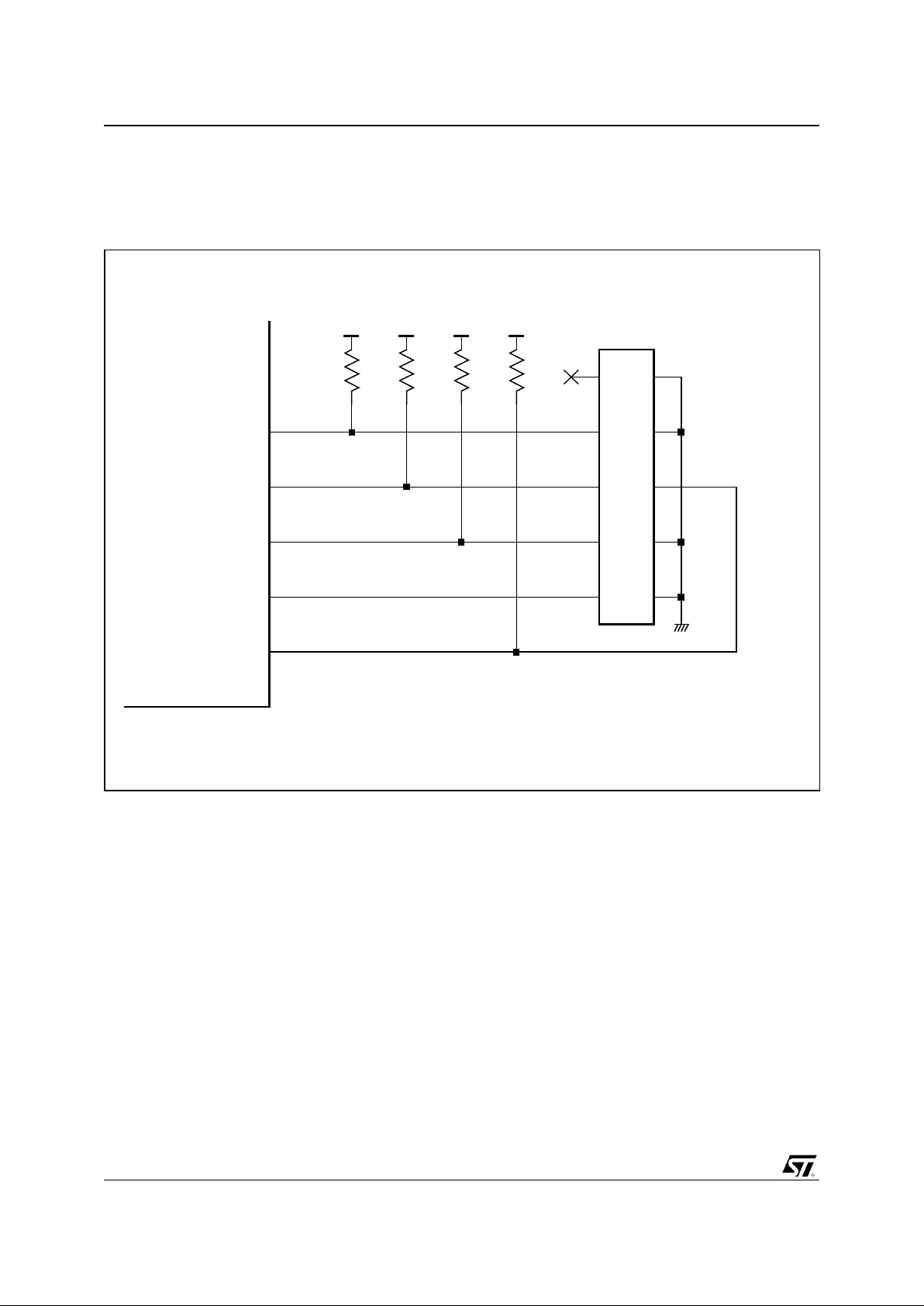
DESIGN GUIDELINES
70/87 Release 1.3 - January 29, 2002
This is preliminary information on a new product now in development or undergoing evaluation. Details are subject to change without notice.
6.3.9. JTAG INTERFACE
The STPC integrat es a JTAG i nterface for scanchain and on-board testing. The only external
device needed are the pull up resistors. Figure 6-
14 describes a typical implementation using these
devices.
Fi
g
ure 6-14.
Typical JTAG implementation
STPC
TCLK
TDO
3V3
Connector
910
12
6
7
34
8
5
TMS
TDI
TRST
3V3 3V3 3V3
Page 71

DESIGN GUIDELINES
Release 1.3 - January 29, 2002 71/87
This is preliminary information on a new product now in development or undergoing evaluation. Details are subject to change without notice.
6.4. PLACE AND ROUTE
RECOMMENDATIONS
6.4.1. GENERAL RECOMMENDATIONS
Some STPC Interfaces run at high speed and
need to be carefully routed or even shielded like:
1) Memor y I n t e rface
2) PCI bus
3) 14 MHz oscillator stage
All clock signals have to be routed first and
shielded for speeds of 27MHz or higher. The h igh
speed signals follow the same constraints, as for
the memory and PCI control signals.
The next interfaces to be routed are M emory and
PCI.
All the analog noise-sensitive signals ha ve to be
routed in a separate area and hence can be
routed indepedently.
Figure 6-15. Shielding signals
ground ring
ground pad
shielded signal line
ground pad
shielded signal lines
Page 72

DESIGN GUIDELINES
72/87 Release 1.3 - January 29, 2002
This is preliminary information on a new product now in development or undergoing evaluation. Details are subject to change without notice.
6.4.2. MEMORY INTERFACE
6.4.2.1. Introduction
In order to achieve SDRAM memory interfaces
which work at clock frequencies of 100 MHz and
above, careful consideration has to be given to the
timing of the interface with all the various electrical
and physical constraints taken i nto consideration.
The guidelines described below are related to
SDRAM components on DIMM modules. For
applications where the memories are directly
soldered to the motherboard, the PCB should be
laid out such that the trace lengths fit within the
constraints shown here. The traces could be
slightly shorter since the extra routing on the
DIMM PCB is no longer present but it is then up to
the user to verify the timings.
6.4.2.2. SDRAM Clocking Scheme
The SDRAM Clocking Scheme deserves a special
mention here. Basically the memory clock is
generated on-chip through a PLL and goes
directly to the MCLKO output pin of the STPC. The
nominal frequency is 100 MHz. Because of the
high load presented to th e M CLK on t he b oard by
the DIMMs it is recommended to rebuffer the
MCLKO signal on the board and balance the skew
to the clock ports of the different DIMMs and the
MCLKI input pin of STPC.
6.4.2.3. Board Layout Issues
The physical layout of the motherboard PCB
assumed in this presentation is as shown in Figure
6-17. Because all of the memory interface sign al
balls are located in the same region of the STPC
device, it is possible to orientate the device to
reduce the trace lengths. The worst case routing
length to the DIMM1 is estimated to be 100 mm.
Solid power and ground planes are a must in order
to provide good return paths for the signals and to
reduce EMI and noise. Also there should be ample
high frequency decoupling between the power
and ground planes to provide a low impedance
path between the planes for the return paths for
signal routings which change layers. If possible,
the traces should be routed adjacent to the s ame
power or ground plane for the length of the trace.
For the SDRAM interface, the most critical signal
is the clock. Any skew between the clocks at the
SDRAM components and the memory controller
will impact the timing budget . In order to get well
matched clocks at all components it is
recommended that all the DIMM clock pins, STPC
Figure 6-16. Clock Scheme
DIMM1
MCLKI
MCLKO
DIMM2
PLL
register
PLL
MA[ ] + Control
MD[63:0]
SDRAM
CONTROLLER
Page 73
DESIGN GUIDELINES
Release 1.3 - January 29, 2002 73/87
This is preliminary information on a new product now in development or undergoing evaluation. Details are subject to change without notice.
memory clock input (MCLKI) and any other
component using the memory clock are
individually driven from a low skew clock driver
with matched routing leng ths. In other words, all
clock line lengths that go from the buffer to the
memory chips (MCLKx) and from the buffer to the
STPC (MCLKI) must be identical.
This is show n in F igure 6-18.
The maximum skew betwe en pins for this part is
250ps. The important factors for the clock buffer
are a consistent drive strength and low skew
between the outputs. The delay through the buffer
is not important so it does not have to be a zero
delay PLL type buffer. The trace lengths from t he
clock driver to the DIMM CKn pins should be
matched exactly. Since the propagation speed
can vary between PCB layers, the clocks should
be routed in a consistent way. The routing to the
STPC memory input should be longer by 75 mm to
compensate for the extra clock routing on the
DIMM. Also a 20 pF capacitor should be placed as
near as possible to the clock input of the STPC t o
compensate for the DIMM’s higher clock load. The
impedance of the t race used for the cl ock routing
should be matched to the DIMM clock trace
impedance (60-75 ohms)
.
To minimise crosstalk
the clocks should be routed with spacing to
adjacent tracks of at least twice the clock trace
width. For designs which use SDRAMs directly
mounted on the motherboard PCB all the clock
trace lengths should be matched exactly.
Figure 6-17. DIMM placement
DIMM2
DIMM1
STPC
35mm
35mm
15mm
10mm
116mm
SDRAM I/F
Figure 6-18. Clock Routing
MCLKO
DIMM CKn input
STPC MCLKI
DIMM CKn input
DIMM CKn input
Low skew clock driver:
L
L+75mm*
20pF
* No additional 75mm when SDRAM directly soldered on board
Page 74

DESIGN GUIDELINES
74/87 Release 1.3 - January 29, 2002
This is preliminary information on a new product now in development or undergoing evaluation. Details are subject to change without notice.
The DIMM sockets shoul d be populated starting
with the furthest DIMM from the STPC device first
(DIMM1). There are two types of DIMM devices;
single-row and dual-row. The dual-row devices
require two chip select signals to select between
the two rows. A STPC device with 4 chip select
control lines could control either 4 single-row
DIMMs or 2 dual-row DIMMs. When only 2 chip
select control lines are activated, only t wo singlerow DIMMs or one dual-row DIMM can be
controlled.
When using DIM M modules, schematics h ave to
be done carefully in order to avoid data buses
completely crossing on the boa rd. This has to be
checked at the library level. In order to achieve the
layout shown in Figure 6-19, schematics hav e to
implement the crossing desc ribed in Figure 6-20.
The DQM signals must be ex changed using the
same order.
6.4.2.4. Summary
For unbuffered DIMMs the address/control signals
will be the m o s t cr iti ca l for ti ming. The sim ula t ion s
show that for these signals the best way to drive
them is to use a parallel termination. For
applications where speed is not so critical series
termination can be used as this will save power.
Using a low impedance such as 50Ω for these
critical traces is recomm ended as it b oth reduces
the delay and the overshoot.
The other memory interface signals will typically
be not as critical as the address/control signals.
Using lower impedance traces is also beneficial
for the other signals but if their timing is not as
critical as the address/control signal s they could
use the default value. Usin g a lower impedance
implies using wider traces which may have an
impact on the routing of the board.
The layout of this interface can be validated by an
electrical simulation using the IBIS model
available on the STPC web site.
Figure 6-19. Optimum Data Bus Layout for DIMM
Figure 6-20. Schematics for Optimum Data Bus Layout for DIMM
DIMM
STPC
SDRAM I/F
D[15:00] D[31:16]
D[47:32] D[63:48]
MD[31:00]
MD[63:32]
MD[15:00],DQM[1:0]
MD[31:16],DQM[3:2]
MD[47:32],DQM[5:4]
MD[63:48],DQM[7:6]
D[15:00],DQM[1:0]
D[31:16],DQM[3:2]
D[47:3 2],DQM[5:4]
D[63:4 8],DQM[7:6]
DIMMSTPC
Page 75

DESIGN GUIDELINES
Release 1.3 - January 29, 2002 75/87
This is preliminary information on a new product now in development or undergoing evaluation. Details are subject to change without notice.
6.4.3. PCI INTERFACE
6.4.3.1. Introduction
In order to achieve a PCI interface which work at
clock frequencies up to 33MHz, careful
consideration has to be given to the timing of the
interface with all the various electrical and
physical constraints taken into consideration.
6.4.3.2. PCI Clocking Scheme
The PCI Clocking Scheme deserves a special
mention here. Basically the PCI clock (PCICLKO)
is generated on-chip from HCLK through a
programmable delay line and a clock divider. The
nominal frequency is 33MHz. This clock must be
looped to PCICLKI and goes t o the internal S outh
Bridge through a des kewer. On the contrary, the
internal North Bridge is clocked by HCLK, putting
some additionnal constraints on T
0
and T1.
Figure 6-21. Clock Scheme
HCLK PLL
1/2
1/3
1/4
clock
Strap Options
PCICLKO
T
1
PCICLKI
HCLK
AD[31:0]
South
North
Deskewer
MUX
T
0
T
2
delay
STPC
MD[30:27] MD[17,4]
MD[7:6]
Bridge
Bridge
Page 76

DESIGN GUIDELINES
76/87 Release 1.3 - January 29, 2002
This is preliminary information on a new product now in development or undergoing evaluation. Details are subject to change without notice.
6.4.3.3. Board Layout Issues
The physical layout of the motherboard PCB
assumed in this presentation is as shown in Figure
6-22. For the PCI interface, the most critical signal
is the clock. Any skew between the clocks at the
PCI components and the STPC will impact the
timing budget. In order to get well matched clocks
at all components it is recommended that all the
PCI clocks are individually driven from a serial
resistance with matched routing lengths. In other
words, all clock line lengths that go from the
resistor to the PCI chips (PCICLKx) must be
identical.
The figure below is for PCI devices soldered onboard. In the case o f a PCI slot, the wire length
must be shortened by 2.5" to compensate the
clock layout on the PCI board. The maximum
clock skew between all devices is 2ns according
to PCI specifications.
The Figure 6-23 describes a typical clock delay
implementation. The e xact timing constraints are
listed in the PCI section of the
Electrical
Specifications
Chapter.
Figure 6-22. Typical PCI clock routing
Length(PCICLKI) = Length(PCICLKx) with x = {A,B,C}
Note: The value of 22 Ohm s corresponds to tracks with Z0 = 70 Ohms.
PCICLKI
PCICLKO
PCICLKA
PCICLKB
PCICLKC
Device A
Device B
Device C
Figure 6-23. Clocks relationships
PCICLKO
PCICLKI
HCLK
PCICLKx
Page 77
DESIGN GUIDELINES
Release 1.3 - January 29, 2002 77/87
This is preliminary information on a new product now in development or undergoing evaluation. Details are subject to change without notice.
6.4.4. THERMAL DISSIPATIO N
6.4.4.1. Power saving
Thermal dissipation of the STPC depends mainly
on supply voltage. When the system does not
need to work at the upper voltage limit, it may
therefore be beneficial to reduce the voltage to the
lower voltage limit, where possible. This could
save a few 100’s of mW.
The second area to look at is unused interfaces
and functions. Depending on the application,
some input signals can be grounded, and some
blocks not powered or shutdown. Clock speed
dynamic adjustment is also a solution that can be
used along with the integrated power
management unit.
6.4.4.2. Thermal balls
The standard way to route thermal balls to ground
layer implements only one via pad for each ball
pad, connected using a 8-mil wire.
With such configuration the P lastic BG A package
does 90% of the t hermal dissipation through the
ground balls, and especially the central thermal
balls which are directly connected to the die. The
remaining 10% is dissipated through the case.
Adding a heat sink reduces this value to 85%.
As a result, some basic rules must be followed
when routing the STPC in order to avoid thermal
problems.
As the whole ground layer acts as a heat sink, the
ground balls must be directly connec ted to it, as
illustrated in Figure 6-24. If one ground layer is not
enough, a second ground plane may be added.
When possible, it is important to avoid other
devices on-board using the PCB for heat
dissipation, like linear regulators, as this would
heat the STPC itself and reduce the temperature
range of the whole system, In case these devices
can not use a separate heat sink, they must not be
located just near the STPC
Figure 6-24. G rou nd routing
Pad for ground ball
Thru hole to ground layer
T
o
p
L
a
y
e
r
:
S
i
g
n
a
l
s
P
o
w
e
r
l
a
y
e
r
I
n
t
e
r
n
a
l
l
a
y
e
r
:
s
i
g
n
a
l
s
B
o
t
t
o
m
L
a
y
e
r
:
g
r
o
u
n
d
l
a
y
e
r
Note: For better visibility, ground balls are not all routed.
Page 78
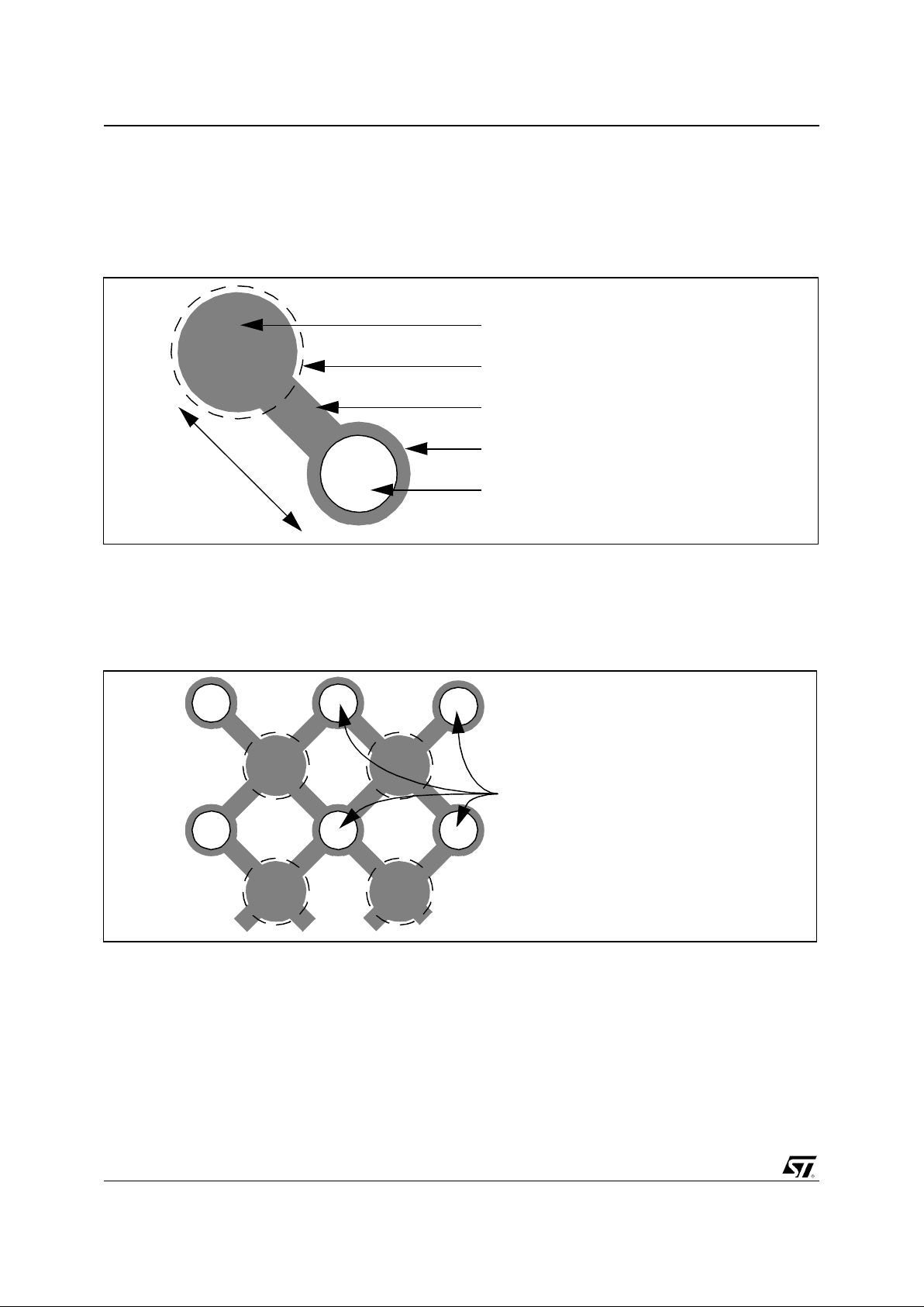
DESIGN GUIDELINES
78/87 Release 1.3 - January 29, 2002
This is preliminary information on a new product now in development or undergoing evaluation. Details are subject to change without notice.
When considering thermal dissipat ion, one of the
most important parts of the layout is the
connection between the ground balls and the
ground layer.
A 1-wire connection is shown in Fi gure 6-25. T he
use of a 8-mil wire results in a thermal resistance
of 105°C/W assuming copper is used (418 W/
m.°K). This high value is due to the thickness (34
µm) of the copper on the external side of the PCB.
Considering only the central matrix of 36 thermal
balls and one via for each ball, the global thermal
resistance is 2.9°C/W. This can be easily
improved using four 12.5 mil wires to connect to
the four vias around the ground pad link as in
Figure 6-26. This gives a total of 49 vias and a
global resistance for the 36 thermal balls of 0.5°C/
W.
The use of a ground plane l ike in Figure 6-27 is
even better.
Figure 6-25. R ecom m ended 1-wire Po wer/Ground Pad Layout
Solder Mask (4 mil)
Pad for ground ball (diameter = 25 mil)
Hole to ground layer (diameter = 12 mil)
Connection Wire (width = 12.5 mil)
Via (diameter = 24 mil)
34.5
mil
1 mil = 0.0254 mm
Figure 6-26. Re commended 4-wi re Ground Pad Lay out
4 via pads for each ground ball
Page 79
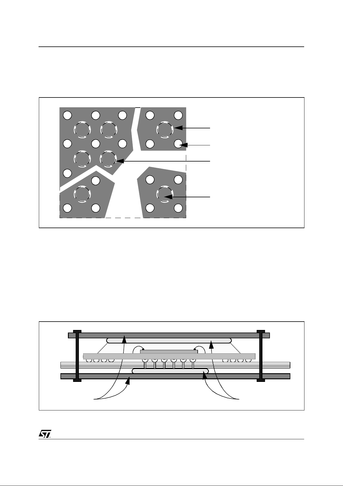
DESIGN GUIDELINES
Release 1.3 - January 29, 2002 79/87
This is preliminary information on a new product now in development or undergoing evaluation. Details are subject to change without notice.
To avoid solder wicking over to t he via pads during
soldering, it is important to have a solder mask of
4 mil around the pad (NSMD pad). This gives a
diameter of 33 mil for a 25 mil ground pad.
To obtain the optimum ground layout, place the
vias directly under the ball pads. In th is case no
local board distortion is tolerated.
6.4.4.3. Heat dissipation
The thickness of the copper on PCB layers is
typically 34 µm for external layers and 17 µm for
internal layers. This means that thermal
dissipation is not good; high board temperat ures
are concentrated around the devices and these
fall quickly with increased distance.
Where possible, place a metal layer inside the
PCB; this improves dramatically the spread of
heat and hence the thermal dissipation of the
board.
The possibility of using the whole system box for
thermal dissipation is very us eful in cases o f high
internal temperatures and low outside
temperatures. Bottom side of the PBGA should be
thermally connected to the metal cha ssis in order
to propagate the heat flow through the metal.
Thermally connecting also the top side will
improve furthermore the heat d issipation. Figure
6-28 illustrate s su c h a n implementation.
Figure 6-27. O pti m um Layout for Central Gro und Ball - top layer
Via to Ground layer
Pad for ground ball
Clearance = 6mil
diameter = 25 mil
hole diameter = 14 mil
Solder mask
diameter = 33 mil
External diameter = 37 mil
connections = 10 mil
Figure 6-28. Use of Metal Plate for Thermal Dissipation
Metal planes Thermal conductor
Board
Die
Page 80
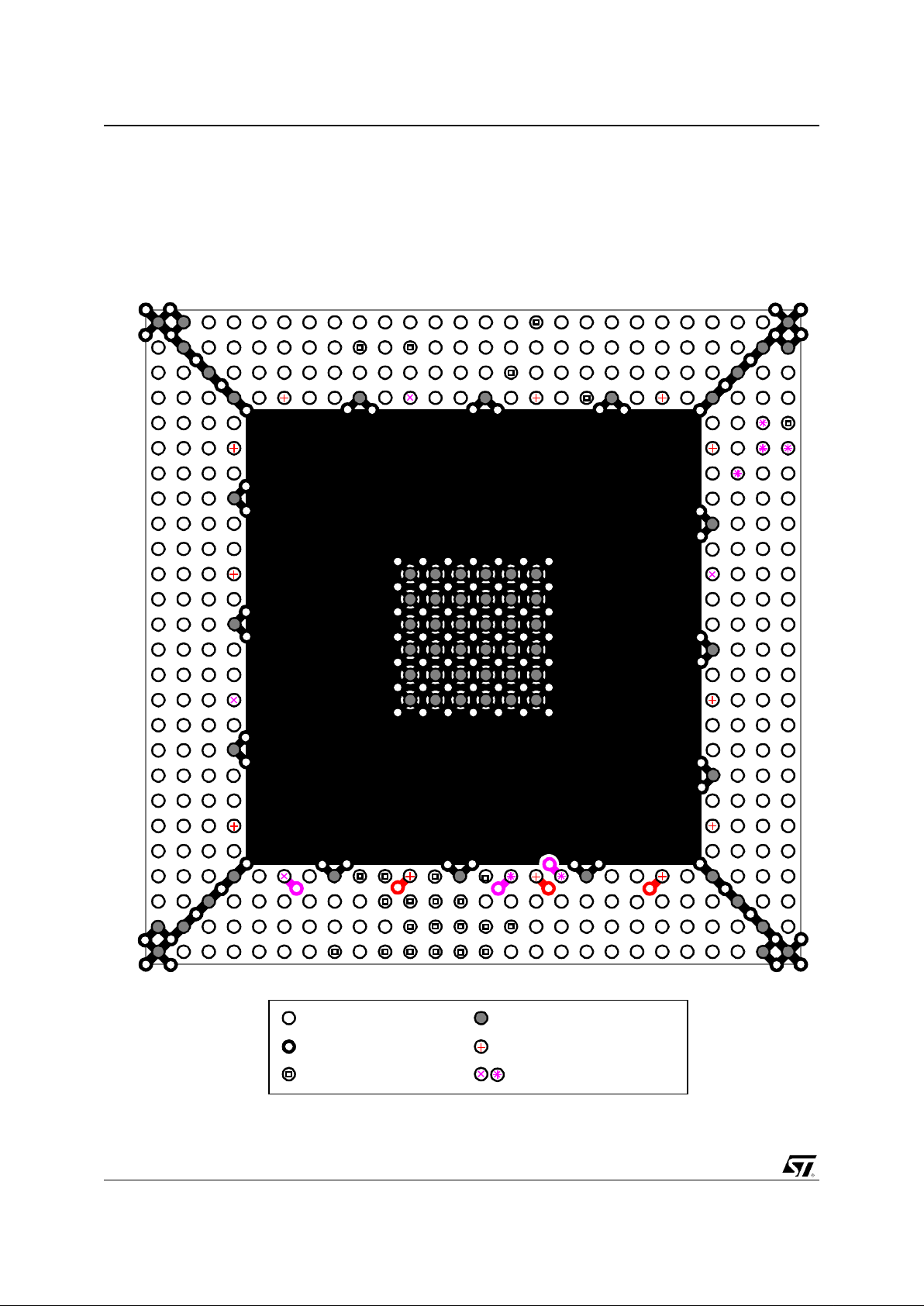
DESIGN GUIDELINES
80/87 Release 1.3 - January 29, 2002
This is preliminary information on a new product now in development or undergoing evaluation. Details are subject to change without notice.
As the PCB acts as a heat sink, the layout of top
and ground layers must be done with care to
maximize the board su rface dissipating the heat.
The only limitation is the risk of losing routing
channels. Figure 6-29 and Figure 6-30 show a
routing with a good thermal dissipation thanks to
an optimized placement of power and signal vias.
The ground plane s hould be on bottom layer for
the best heat spreading (thicker layer than internal
ones) and dissipation (direct contact with air). .
Figure 6-29. Layout for Good Thermal Dissipation - top layer
1
A
3.3V ball
2.5V ball (Core / PLLs)
Via
STPC ball
GND ba ll
Not Connected ball
Page 81

DESIGN GUIDELINES
Release 1.3 - January 29, 2002 81/87
This is preliminary information on a new product now in development or undergoing evaluation. Details are subject to change without notice.
Figure 6-30. Recommend signal wiring (top & ground layers) with corresponding heat flow
STPC balls
External row
Interna l row
GND PowerPower
Page 82

DESIGN GUIDELINES
82/87 Release 1.3 - January 29, 2002
This is preliminary information on a new product now in development or undergoing evaluation. Details are subject to change without notice.
6.5. DEBUG METHOD OL OGY
In order to bring a STPC-based board to life with
the best efficiency, it is recommended to follow the
check-list described in this section.
6.5.1. POWER SU PPL IES
In parallel with the assembly process, it is useful to
get a bare PCB to check the potential shortcircuits between the various power and ground
planes. This test is also recomm ended when the
first boards are back from assembly. This will
avoid bad surprises in case of a short-circuit due
to a bad soldering.
When the system is powered, all power supplies,
including the PLL power pins must be checked t o
be sure the right level is present. See Table 4-2 for
the exact supported voltage range:
VDD_CORE: 2.5V
VDD_xxxPLL: 2.5V
VDD: 3.3V
6.5.2. BOOT SEQUENCE
6.5.2.1. Reset input
The checking of the reset sequence is the next
step. The waveform of SYSRSTI# must complies
with the timings described in Figure 4-3. This
signal must not have glitches an d must stay low
until the 14.31818MHz outpu t (OSC14 M) is at the
right frequency and the strap options are
stabilized to a valid configuration.
In case this clock is not present, check the 14MHz
oscillator stage (see Figure 6-3).
6.5.2.2. Strap options
The STPC has been d esigned in a way to allow
configurations for test purpose that differs from the
functional configuration. In many cases, the
troubleshootings at this stage of the debug are the
resulting of bad strap options. This is why it is
mandatory to check they are properly setup and
sampled during the boot sequence.
The list of all the strap options is summarized at
the beginning of Section 3.
6.5.2.3. Clocks
Once OSC14M is checked and correct, the next
signals to measure are the Host clock (HCLK),
PCI clocks (PCI_CLKO, PCI_CLKI) and Memory
clock (MCLKO, MCLKI).
HCLK must run at the speed defined by the
corresponding strap options (see Table 3-1) and
must not be more than 100MHz. In x2 CPU c lock
mode, this clock must be limited to 66MHz.
PCI_CLKI and PCI_CLK O m ust be c onnected as
described in Figure 6-19 and not be higher than
33MHz. Their speed depends on HCLK and on
the divider ratio defined by the
MD[4] and MD[17]
strap options as described in Section 3.
To ensure a correct behaviour of the device, the
PCI deskewing logic must b e configured properly
by the MD[7:6] strap options according to Sect ion
3. For timings constraints, refers to Section 4.
MCLKI and MCLKO must be connected as
described in Figure 6-3 to Figure 6-5 depending
on the SDRAM implementation. The memory
clock must run at HCLK speed when in
synchronous mode and must not be higher than
100MHz in any case.
6.5.2.4. Reset output
If SYSRSTI# and all clocks are correct, then the
SYSRSTO# output signal should behave as
described in Figure 4-3
.
6.5.3. ISA MODE
Prior to check the ISA bus control signals,
PCI_CLKI, ISA_CLK, ISA_CLK2X, and DEV_CLK
must be running properly. If it is not the case, it is
probably because one of the previou s steps has
not been completed.
6.5.3.1. First code fetches
When booting on the ISA bus, the two key signals
to check at the very beginning are RMRTCCS#
and FRAME#.
The first one is a Chip Select for the boot flash
and is multiplexed with the IDE interface. It should
toggle together with ISAOE# and MEMRD# to
fetch the first 16 bytes of code. This corresponds
to the loading of the first line of the CPU cache.
In case RMRTCCS# does not toggle, it is then
necessary to check the PCI FRAME# signal.
Indeed the ISA controller is part of the South
Bridge and all ISA bus cy cles are visible on the
PCI bus.
If there is no activity on the P CI bus, then one of
the previous steps has not been checked properly.
If the re is activ ity then th ere must be someth ing
conflicting on the ISA bus or on the PCI bus.
6.5.3.2. Boot Flash size
The ISA bus supports 8-bit and 16-bit memory
devices. In case of a 16-bit boot flash, the signal
MEMCS16# must be activated during
Page 83

DESIGN GUIDELINES
Release 1.3 - January 29, 2002 83/87
This is preliminary information on a new product now in development or undergoing evaluation. Details are subject to change without notice.
RMRTCCS# cycle to inform the ISA controller of a
16-bit device.
6.5.3.3. POST code
Once the 16 first bytes are fetched and decoded,
the CPU core continue its execution depending on
the content of these first data. Usually, it
corresponds to a JUMP instruction and the code
fetching continues, generating read cycles on the
ISA bus.
Most of the BIOS and boot loaders are reading the
content of the f lash, decompressing it in SDRA M,
and then continue the execution by jumping to the
entry point in RAM. This boot process ends with a
JUMP to the entry point of the OS launcher.
These various steps of the booting sequence are
codified by the so-called POST codes (Power-On
Self-Test). A 8-bit code is written to the port 80H at
the beginning of each stage of the booting process
(I/O write to address 0080H) and can be displayed
on two 7-segment display, enabl ing a fast visual
check of the booting completion level.
Usually, the last POST code is 0x00 and
corresponds to the jump into the OS launcher.
When the execution fails or hangs, the lastest
written code stays visible on that display,
indicating either the piece of code to analyse,
either the area of the hardware not working
properly.
6.5.4. LOCAL BUS MODE
As the Local Bus controller is located into the Host
interface, there is no access to the cycles on the
PCI, reducing the amount of signals to check.
6.5.4.1. First code fetches
When booting on the Local Bu s, the key signal to
check at the very beginning is FCS 0#. This sig nal
is a Chip Select for the boot flash and should
toggle together with PRD# to fetch the first 16
bytes of code. This correspon ds t o the l oading of
the f irst li ne of t he CPU cache.
In case FCS0# does n ot toggle, then one of the
previous steps has not been done properly, like
HCLK speed and CPU clock multiplier (x1, x2).
6.5.4.2. Boot Flash size
The Local Bus support 16-bit boot memory
devices only.
6.5.4.3. POST code
Like in ISA mode, POST codes can be
implemented on the Loca l Bus. The difference is
that an IOCS# must be programmed at I/O
address 80H prior to writing these code, the POST
display being connected to this IOCS# and to the
lower 8 bits of the bus.
6.5.5. SUMMARY
Here is a check-list for the STPC board debug
from power-on to CPU execution.
For each step, in case of failure, verify first the
corresponding balls of the STPC:
- check if the voltage or activity is correct
- search for potential shortcuts.
For troubleshooting in steps 5 to 10, verify the
related strap options:
- value & connection. Refer to Section 3.
- see Figur e 4-3 for timing constraints
Steps 8a and 9a are for debug in ISA mode while
steps 8b and 9b are for Local Bus mode.
Check: H ow? Troubleshooting
1
Power
supplies
Verify that voltage is within specs:
- this must include HF & LF noise
- avoid full range sweep
Refer to Table 4-1 for values
Measure voltage near STPC balls:
- use very low GND connection.
Add some decoupling capacitor:
- the smallest, the nearest to STPC balls.
2 14.318 MHz Verify OSC14M speed
The 2 capacitors used with the quartz must
match with the capacitance of the crystal.
Try other values.
3
SYSRSTI#
(Power Good)
Measure SYSRSTI# of STPC
See
Figure 4-3
for waveforms.
Verify reset generation circuit:
- device reference
- components value
5 HCLK
Measure HCLK is at selected frequency
25MHz < HCLK < 100MHz
HCLK wire must be as short as possible
Page 84

DESIGN GUIDELINES
84/87 Release 1.3 - January 29, 2002
This is preliminary information on a new product now in development or undergoing evaluation. Details are subject to change without notice.
6 PCI clocks
Measure PCICLKO:
- maximum is 33MHz by standard
- check it is at selected frequency
- it is generated from HCLK by a division
(1/2, 1/3 or 1/4)
Check PCICLKI equals PCICLKO
Verify PCICLKO loops to PCICLKI.
Verify maximum skew between any PCI clock
branch is below 2ns.
In Synchronous mode, check MCLKI.
7
Memory
clocks
Measure MCLKO:
- use a low-capacitance probe
- maximum is 100MHz
- check it is at selected frequency
- In SYNC mode MCLK=HCLK
- in ASYNC mode, default is 66MHz
Check MCLKI equals MCLKO
Verify load on MCLKI.
Verify MCLK programming (BIOS setting).
4 SYSRSTO#
Measure SYSRSTO# of STPC
See
Figure 4-3
for waveforms.
Verify SYSRSTI# duration.
Verify SYSRSTI# has no glitch
Verify clocks are running.
8a PCI cycles
Check PCI signals are toggling:
- FRAME#, IRDY#, TRDY#, DEVSEL#
- these signals are active low.
Check, with a logic analyzer, that first
PCI cycles are the expected ones:
memory read starting at address with
lower bits to 0xFFF0
Verify PCI slots
If the STPC don’t boot
- verify data read from boot memory is OK
- ensure Flash is correctly programmed
- ensure CMOS is cleared.
9a
ISA
cycles
to
boot memory
Check RMRTCCS# & MEMRD#
Check directly on boot memory pin
Verify MEMCS16#:
- must not be asserted for 8-bit memory
Verify IOCHRDY is not be asserted
Verify ISAOE# pin:
- it controls IDE / ISA bus demultiplexing
8b
Local Bus
cycles
to
boot memory
Check FCS0# & PRD#
Check directly on boot memory pin
Verify HCLK speed and CPU clock mode.
9b
Check, with a logic analyzer, that first
Local Bus cycles are the expected one:
memory read starting at the top of boot
memory less 16 bytes
If the STPC don’t boot
- verify data read from boot memory is OK
- ensure Flash is correctly programmed
- ensure CMOS is cleared.
10
The CPU fills its first cache line by fetching 16 bytes from boot memory.
Then, first instructions are executed from the CPU.
Any boot memory access done after the first 16 bytes are due to the instructions executed by the CPU
=> Minimum hardware is correctly set, CPU executes code.
Please have a look to the Bios Writer’s Guide or Programming Manual to go further with your board testing.
Check: How? Troubleshooting
Page 85
ORDERING DATA
Release 1.3 - January 29, 2002 85/87
This is preliminary information on a new product now in development or undergoing evaluation. Details are subject to change without notice.
7. ORDERING DATA
7.1. ORDERING CODES
ST PC E1 E E B C
STMicroelectronics
Prefix
Product Family
PC: PC Compatible
Product ID
E1: Elite
Core Speed
E: 100 MHz
H: 133 MHz
Memory Interface Speed
E: 100 MHz
D: 90 MHz
Package
B: 388 Overmoulded BGA
Temperature Range
C: Commercial
Case Temperature (Tcase) = 0°C to +85°C
I: Industrial
Case Temperature (Tcase) = -40°C to +115°C
Page 86

ORDERING DATA
86/87
Release 1.3 - Januar
y
29, 2002
This is preliminary information on a new product now in development or undergoing evaluation. Details are subject to change without notice.
7.2. AVAILABLE PART NUMBERS
7.3. CUSTOMER SERVICE
More information is available on the
STMicroelectronics Internet site
http://
www.st.com/stpc
Part Number
Core Frequency
( MHz )
CPU Mode
( X1 / X2 )
Memory Interface
Speed (MHz)
Tcase Range
( °C )
STPCE1EEBC 100 X 1 100
0°C to +85°
STPCE1HDBC 133 X2 90
STPCE1EEBI 100 X1 100
-40°C to +115°
STPCE1HDBI 133 X2 90
Page 87

Information furnished is believed to be accurate and reliable. However, STMicroelectronics assumes no responsibility for the consequences
of use of such information nor for any infringement of patents or other rights of third parties which may result from its use. No license is granted
by implic ation or otherwise unde r any patent or patent right s of STMicroelectronics. Specifications menti oned in this publication are subject
to change without notice. This publication supersedes and replaces all information previously supplied. STMicroelectronics products are not
authorized for use as crit i cal components i n l i f e support devices or systems without express written appr oval of STMicroe l ectronics.
© 2000 STMicroelectronics - All Rights Reserved
The ST logo is a registered trademark of S T M i croelectronics.
All other na m es are the property of their respective owner s.
STMicroelectronics GROUP OF COMPANIES
Australia - Brazil - China - France - Germany - Italy - Japan - Korea - Malaysia - Malta - Mexico - Morocco - The Netherlands - Singapore -
Spain - Sweden - Switzerland - Taiwan - Th ai land - United Kingdom - U.S . A.
87
Release 1.3
This is preliminary information on a new product now in development or undergoing evaluation. Details are subject to change without notice.
 Loading...