

Page 1
STPC CONSUMER-S
PC Compatible Embeded Microprocessor
ADVANCED DATA
1/5129/10/99
Release B
This is preliminary information on a new product now in development or undergoing evaluation. Details are subject to change without notice.
Figure 1. Logic Diagram
■ POWERFUL x86 PROCESSOR
■ 64-BIT 66MHz SDRAM UMA CONTROLLER
■ VGA & SVGA CRT CONTROLLER
■ 2D GRAPHICS ENGINE
■ VIDEO INPUT PORT
■ VIDEO PIPELINE
- UP-SCALER
- VIDEO COLOR SPACE CONVERTER
- CHROMA & COLOUR KEY SUPPORT
■ TV OUTPUT
- 3-LINE FLICKER FILTER
- CCIR 601/656 SCAN CONVERTER
- NTSC / PAL COMPOSITE, RGB, S-VIDEO
■ PCI MASTER / SLAVE CONTROLLER
■ ISA MASTER / SLAVE CONTROLLER
■ INTEGRATED PERIPHERAL CONTROLLER
- DMA CONTROLLER
- INTERRUPT CONTROLLER
- TIMER / COUNTERS
■ OPTIONAL 16-BIT LOCAL BUSINTERFACE
■ EIDE CONTROLLER
■ I C INTERFACE
■ POWER MANAGEMENT UNIT
■ 3.3V OPERATION
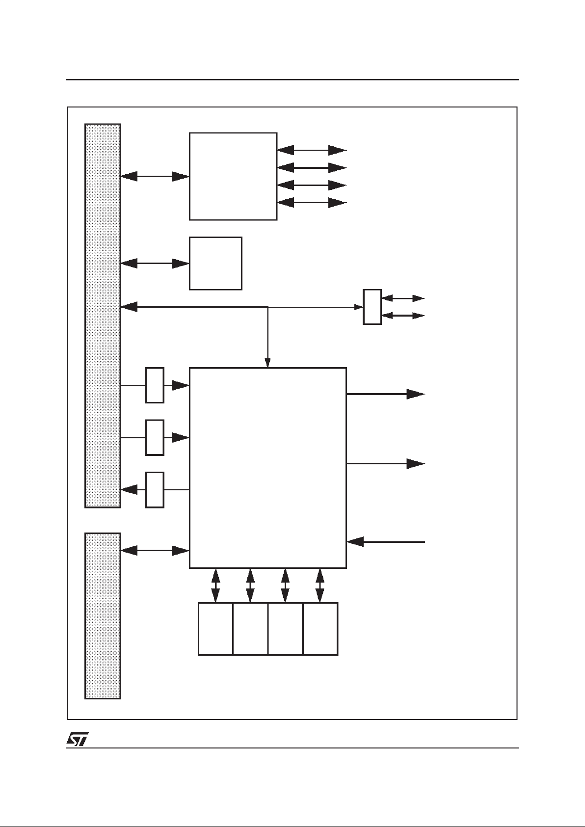
STPC CONSUMER-S OVERVIEW
The STPC Consumer-S integrates a standard 5th
generation x86 core, a Synchronous DRAM controller, a graphics subsystem, a video input port,
video pipeline, and support logic i ncluding PCI,
ISA, and IDE controllers to provide a s ingle consumer orientated PC compatible subsystem on a
single device.
The device is based on a tightly coupled U nified
Memory Architecture (UMA), sharing the same
memory array between the CPU main memory
and the graphics and video frame buffers.
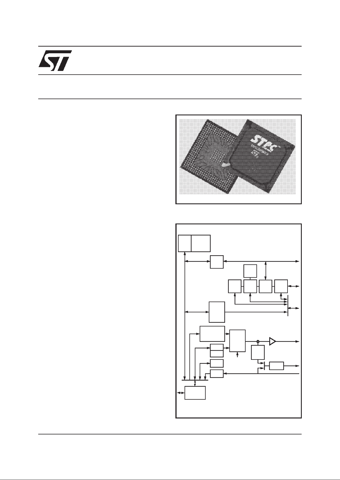
The STPC Consumer-S is packaged in a 388
Plastic Ball Grid Array (PBGA).
PBGA3 88
x86
Core
Host
I/F
SDRAM
CTRL
SVGA
GE
VIP
PCI
m/s
LB
CTR
PCI Bus
ISA
m/s
IPC
PCI
m/s
ISA Bus
CRTC
Cursor
Moni tor
TV
IDE
I/F
PMU
W.dog
Video
Pipeline
C Key
K Key
LUT
Local Bus
Encoder
TVO
Page 2

STPC CONSUMER-S
2/51
Release B
This is preliminary information on a new product now in development or undergoing evaluation. Details are subject to change without notice.
■ X86 Processor core
■ Fully static 32-bit 5-stage pipeline, x86
processor fully PC compatible.
■ Can access up to 4GB of external memory.
■ 8Kbyte unified instruction and data cache
with write back and write through capability.
■ Parallelprocessing integral floating pointunit,
with automatic power down.
■ Fully static design for dynamic clock control.
■ Low power and system management modes.
■ SDRAM Controller
■ 64-bit data bus.
■ Up to 66MHz SDRAM clock speed.
■ Integrated system memory, graphic frame
memory and video frame memory.
■ Supports 2MB up to 128 MB memory.
■ Supports 8MB, 16M, and 32MB DIMMs.
■ Supports buffered, non buffered,and
registered DIMMs
■ 4-line write buffersfor CPUto DRAM and PCI
to DRAM cycles.
■ 4-line read prefetch buffers for PCI masters.
■ Programmable latency
■ Programmable timing for DRAM parameters.
■ Supports -8, -10, -12, -13, -15 memory parts
■ Supports 1MB up to 8MB memory hole.
■ 32-bit accesses not supported.
■ Autoprecharge not supported.
■ Power down not supported.
■ FPM and EDO not supported.
■ Graphics Controller
■ 64-bit windows accelerator.
■ Compatibility to VGA & SVGA standards.
■ Hardware acceleration for text, bitblts,
transparent blts and fills.
■ Up to 64 x 64 bit graphics hardware cursor.
■ Up to 4MB long linear frame buffer.
■ 8-, 16-, and 24-bit pixels.
■ CRT Controller
■ Integrated 135MHz triple RAMDAC allowing
for 1024 x 768 x 75Hz display.
■ 8-, 16-, 24-bit pixels.
■ Interlaced or non-interlaced output.
■ Video Input port
■ Accepts video inputs in CCIR 601 mode.
■ Optional 2:1 decimator
■ Stores captured video in off setting area of
the onboard frame buffer.
■ Video pass through to the onchip PAL/NTSC
encoder for full screen video images.
■ HSYNC and B/T generation or lock onto
external video timing source.
■ Video Pipeline
■ Two-tapinterpolative horizontal filter.
■ Two-tapinterpolative vertical filter.
■ Color space conversion.
■ Programmable window size.
■ Chroma and color keying for integrated video
overlay.
■ TV Output
■ Programmable two tap filter with gamma
correction or three tap flicker filter.
■ Progressiveto interlaced scan converter.
■ NTSC-M, PAL-M,PAL-B,D,G,H,I,PAL-N easy
programmable video outputs.
■ CCIR601 encoding with programmable color
subcarrier frequencies.
■ Line skip/insert capability
■ Interlaced or non-interlaced operation mode.
■ 625 lines/50Hz or 525 lines/60Hz 8 bit
multiplexedCB-Y-CR digital input.
■ CVBS and R,G,B simultaneous analog
outputs through 10-bit DACs.
■ Cross color reductionby specific trap filtering
on luma within CVBS flow.
■ Power down mode available on each DAC.
Page 3

STPC CONSUMER-S
3/51
Release B
This is preliminary information on a new product now in development or undergoing evaluation. Details are subject to change without notice.
■ PCI Controller
■ Fully compliant with PCI 2.1 specification.
■ Integrated PCI arbitration interface. Up to 3
masters can connect directly. External PAL
allows forgreater than 3masters.
■ Translation of PCI cycles to ISA bus.
■ Translation of ISA master initiated cycle to
PCI.
■ Support forburst read/write from PCI master.
■ PCI clock is 1/3 or 1/2 Host clock .
■ ISA master/slave controller
■ Generates the ISA clock from either
14.318MHz oscillator clock or PCI clock
■ Supports programmable extrawait state for
ISA cycles
■ Supports I/O recovery time for back to back I/
O cycles.
■ Fast Gate A20 and Fast reset.
■ Supports the single ROM that C, D,or E.
blocks shares with F blockBIOS ROM.
■ Supports flash ROM.
■ Supports ISA hidden refresh.
■ Buffered DMA &ISA master cycles to reduce
bandwidth utilization of thePCI andHost bus.
NSP compliant.
■ Integrated Peripheral Controller
■ 2X8237/AT compatible 7-channel DMA
controller.
■ 2X8259/AT compatible interrupt Controller.
16 interrupt inputs - ISAand PCI.
■ Three 8254 compatible Timer/Counters.
■ Co-processor error support logic.
■ Supports external RTC.
■ Local Bus interface
■ Multiplxed with ISA interface.
■ Low latency bus
■ 22-bit address bus.
■ 16-bit data bus with word steering capability.
■ Programmable timing (Host clockgranularity)
■ 2 Programmable Flash Chip Select.
■ 5 Programmable I/O Chip Select.
■ Supports 32-bit Flashburst.
■ 2-level hardwarekeyprotection forFlash boot
block protection.
■ Supports 2 banksof 8MB flash devices with
boot block shadowed to 0x000F0000.
■ IDE Interface
■ Supports PIO and Bus Master IDE
■ Supports up to Mode 5 Timings
■ Transfer Rates to 22 MBytes/sec
■ Supports up to 4 IDE devices
■ Concurrent channel operation (PIO & DMA
modes) - 4 x 32-Bit Buffer FIFO per channel
■ Support for PIO mode 3 & 4.
■ Support for DMA mode 1 & 2.
■ Support for 11.1/16.6 MB/s,I/O Channel
Ready PIO data transfers.
■ Supports 13.3/16.6 MB/s DMA data transfers
■ Bus Master with scatter/gather capability
■ Multi-word DMA support for fast IDE drives
■ Individual drive timing for all four IDEdevices
■ Supports both legacy & native IDE modes
■ Supports hard drives larger than 528MB
■ Support for CD-ROM and tape peripherals
■ Backward compatibilitywith IDE (ATA-1).
■ Power Management
■ Four powersaving modes: On, Doze,
Standby, Suspend.
■ Programmable system activity detector
■ Supports SMM.
■ Supports STOPCLK.
■ Supports IO trap & restart.
■ Independent peripheral time-out timer to
monitor hard disk, serial & parallel ports.
■ Supports RTC,interrupts and DMAs wake-up
Page 4

GENERAL DESCRIPTION
4/51
Release B
This is preliminary information on a new product now in development or undergoing evaluation. Details are subject to change without notice.
1 GENERAL DESCRIPTION
At the heart of the STPC Consumer-S is an advanced 64-bit processor block, dubbed the
5ST86. The 5ST86 includes a 486 processor core
along with a 64-bit SDRAM controller, advanced
64-bit accelerated graphics and video controller, a
high speed PCI local-bus controller and Industry
standard PC chip set functions (Interrupt controller, DMA Controller, Interval timer and ISA bus).
The STPC Consumer-S makes use of a tightly
coupled Unified Memory Architecture (UMA),
where the same memory array is used for CPU
main memory and graphics frame-buffer. This
means areduction in total system memoryfor system performances that are equal to that of a comparable frame buffer and system memory based
system, and generally much better, due to the
higher memory bandwidth allowed by attaching
the graphics engine directly to the 64-bit processor hostinterface runningat the speed of theprocessor bus rather than the traditional PCI bus.
The 64-bit wide memory array provides the system with 528MB/speak bandwidth. This allowsfor
higher resolution screens andgreater color depth.
The ‘standard’ PC chipset functions (DMA, interrupt controller, timers, power management logic)
are integrated together with the x86 processor
core; additional functions such as communications ports are accessed by the STPC ConsumerS via internal ISA bus.
The PCI bus is the main data communication link
to the STPC Consumer-S chip. The STPC Consumer-S translates appropriate host bus I/O and
Memory cycles onto the PCI bus. It also supports
generation ofConfiguration cycles on the PCI bus.
The STPC Consumer-S, as a PCI bus agent (host
bridge class), fully complies with PCI specification
2.1. The chip-set also implements the PCI mandatory header registers in Type 0 PCI configuration
space for easy porting of PCI aware system BIOS. The devicecontains a PCI arbitration function
for three external PCI devices.
The STPC Consumer-S has two functionnal
blocks
sharing the same balls
: The ISA / IPC /
IDE block and the Local Bus / IDE block (see Table 3). Any board with the STPC Consumer-S
should be built usingonly oneof these two configurations.
At reset, the configuration is done by ‘strap options’ which initialises the STPC Consumer-S to
the right settings. It is a set of pull-up or pull-down
resistors on the memory data bus, checked on reset, which auto-configure theSTPC Consumer-S.
GRAPHICS FUNCTIONS
Graphics functions are controlled through the onchip SVGA controller and the monitor display is
produced through the 2D graphics display engine.
This Graphics Engine is tuned to work with the
host CPU to provide a balanced graphics system
with a low silicon area cost. It performs limited
graphics drawing operations which include hardware acceleration of text, bitblts, transparent blts
and fills. The results of these operations change
the contents of the on-screen or off-screen frame
buffer areas of DRAM memory. The frame buffer
can occupy a space up to 4 Mbytes anywhere in
the physical main memory and always starts from
the bottom of the main physical memory.
The graphics resolution supported is a maximum
of 1280x1024 in 65536 colours and 1024x768 in
true color at 75Hz refresh rate and is VGA and
SVGA compatible. Horizontal timing fields are
VGA compatible while the vertical fields are extended by one bit to accommodate above display
resolution.
VIDEO FUNCTIONS
The STPC Consumer-S provides several additional functions to handle MPEG or similar video
streams. The Video Input Port accepts an encoded digital video stream in one of a number of industry standard formats, decodes it, optionally
decimates it, and deposits it into an off screen
area of the frame buffer. An interrupt request can
be generated when an entire field or frame has
been captured. The video output pipeline incorporates a video-scaler and color space converter
function and provisions in the CRT controller to
display a video window. While repainting the
screen the CRT controller fetches both the video
as well as the normal non-video frame buffer in
two separate internal FIFOs. The video stream
can be color-space converted (optionally) and
smooth scaled. Smooth interpolative scaling in
both horizontal and vertical direction are implemented. Color and Chroma key functions are also
implemented to allow mixing video stream with
non-video frame buffer.
The video output passes directly to the RAMDAC
for monitor output or through another optional
color spaceconverter (RGBto 4:2:2 YCrCb) to the
programmable anti-flicker filter. The flicker filter is
configured as either a two line filter with gamma
correction (primarily designed for DOS type text)
or a 3 line flicker filter (primarily designed for Windows type displays). Thefliker filter is optional and
can besoftware disabled foruse with large screen
area’s of video.
Page 5

GENERAL DESCRIPTION
5/51
Release B
This is preliminary information on a new product now in development or undergoing evaluation. Details are subject to change without notice.
The Video output pipeline of the STPC ConsumerS interfaces directly to the internal digital TV encoder. It takes a 24 bit RGB non-interlaced pixel
stream and converts to a multiplexed 4:2:2 YCrCb
8 bit output stream, the logic includes a progressive to interlaced scan converter and logic to insert appropriate CCIR656 timing reference codes
into the outputstream. It facilitates the high quality
display of VGA or full screen video streams received via the Video input port to standard NTSC
or PAL televisions.
The digital PAL/NTSC encoder outputs interlaced
or non-interlaced video in PAL-B,D,G,H,I PAL-N,
PAL-M or NTSC-Mstandards and “NTSC- 4.43” is
also possible.
The four frame (for PAL) or 2 frame (for NTSC)
burst sequences are internally generated, subcarrier generation being performed numerically with
CKREF as reference. Rise and fall times of synchronisation tips and burst envelope are internally
controlled according to the relevant ITU-R and
SMPTE recommendations.
Video output signals are directed to four analog
output pins through internal D/A convertersgiving,
simultaneous R,G,B and composite CVBS outputs.
IDE INTERFACE
An industry standard EIDE (ATA 2) controller is
built into the STPC Consumer-S. The IDE port is
capable of supporting a total of four devices.
POWER MANAGEMENT
The STPC Consumer-Score is compliantwith the
Advanced Power Management (APM) specification to provide a standard method by which the
BIOS can control the power used by personal
computers. The Power Management Unit module
(PMU) controls the power consumption providing
a comprehensive set of features that control the
power usage and supports compliance with the
United States Environmental Protection Agency’s
Energy Star Computer Program. The PMU provides following hardware structures to assist the
software in managing the power consumption by
the system.
- System Activity Detection.
- Three power down timers.
- Doze timer for detecting lack of system activity
for short durations.
- Stand-by timer for detecting lack of system activity for medium durations
- Suspend timer for detectinglack of system activity for long durations.
- House-keeping activity detection.
- House-keeping timerto cope with short bursts of
house-keeping activity while dozing or in stand-by
state.
- Peripheral activity detection.
- Peripheral timer for detecting lack of peripheral
activity
- SUSP# modulation to adjust the system performance in various power down states of the system
including full power on state.
- Power control outputs to disable power from different planes of the board.
Lack of system activity for progressively longer
period of times is detected by the three power
down timers. These timers can generate SMI interrupts to CPU so that the SMM software can put
the system in decreasing states of power consumption. Alternatively, system activity in apower
down statecan generateSMI interrupt toallow the
software to bring the system back up to full power
on state. The chip-set supports up to three power
down states: Doze state, Stand-by state and Suspend mode. These correspond to decreasing levels of power savings.
POWER DOWN
Power downputs theSTPC Consumer-S into suspend mode. The processor completes execution
of thecurrent instruction, any pending decoded instructions and associated bus cycles. During the
suspend mode, internal clocks are stopped. Removing power down, the processor resumes instruction fetching and begins execution in the instruction stream at the point it had stopped. Because of the static nature of the core, no internal
data is lost.
Page 6

GENERAL DESCRIPTION
6/51
Release B
This is preliminary information on a new product now in development or undergoing evaluation. Details are subject to change without notice.
Figure 2. Functionnal description.
x86
Core
Host
I/F
SDRAM
I/F
SVGA
GE
VIP
PCI m/s
Local
Bus I/F
PCI BUS
ISA
m/s
IPC
82C206
PCI m/s
ISA Bus
CRTC
HW Cursor
Monitor
TV
- Pixel formating
- Scaler
- Colour Space
IDE
I/F
PMU
watch-
Video Pipeline
Colour Key
Chroma Key
LUT
Local Bus
NTSC/PAL
Encoder
TVO
- CSC
-FF
- CCIR
CCIR Input
Page 7
GENERAL DESCRIPTION
7/51
Release B
This is preliminary information on a new product now in development or undergoing evaluation. Details are subject to change without notice.
Figure 3. Typical Application
STPC Consumer-S
ISA
PCI
4x 16-bit SDRAMs
Super I/O
2x EIDE
Flash
Keyboard / Mouse
Serial Ports
Parallel Port
Floppy
Monitor
TV
Video
SVGA
CCIR601
CCIR656
S-VHS
RGB
PAL
NTSC
IRQ
DMA.REQ
DMA.ACK
DMUX
DMUX
MUX
MUX
RTC
Page 8

GENERAL DESCRIPTION
8/51
Release B
This is preliminary information on a new product now in development or undergoing evaluation. Details are subject to change without notice.
Page 9

Update History for Video controller chapter
9/51
Release B
1.1 UPDATE HISTORY FOR VIDEO CONTROLLER CHAPTER
The following changes have been made to the General Description Chapter on 29/10/99.
Section Change Text
1 Removed
“The STPC Consumer-S has in addition to the 5ST86 a TFT output, a Local
Bus interface, a WatchDog and a JTAG interface.”
Page 10
PIN DESCRIPTION
10/51
Release B
This is preliminary information on a new product now in development or undergoing evaluation. Details are subject to change without notice.
2 PIN DESCRIPTION
2.1 INTRODUCTION
The STPC Consumer-S integrates most of the
functionalities of the PC architecture. As a result,
many of the traditional interconnections between
the host PC microprocessor and the peripheral
devices are totally internal to the STPC Consumer-S. This offers improved performance due to the
tight coupling of the processor core and these peripherals. As aresult many of the externalpin connections are madedirectlyto the on-chipperipheral functions.
Figure 2.1 shows the STPC Consumer-S external
interfaces. It defines the main busses and their
function. Table 2.1 describes the physical implementation listing signals type and their functionality. Table 2.2 provides a full pin listing and description of pins. Table 2.5 provides a full listing of pin
locations of the STPC Consumer-S package by
physical connection.
Note: Several interface pins are multiplexed with
other functions, refer to Table 2.3 and Table 2.4
for further details
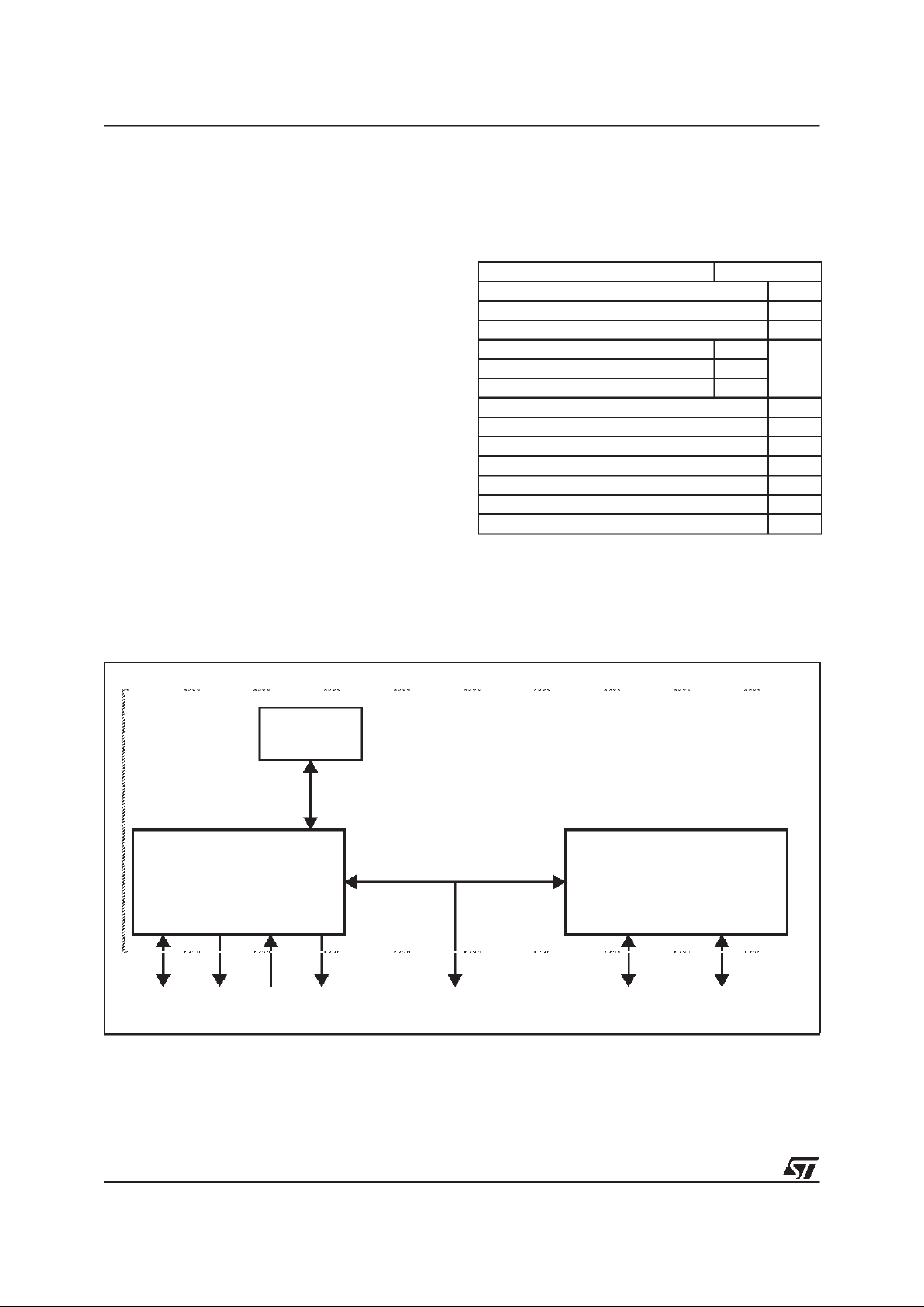
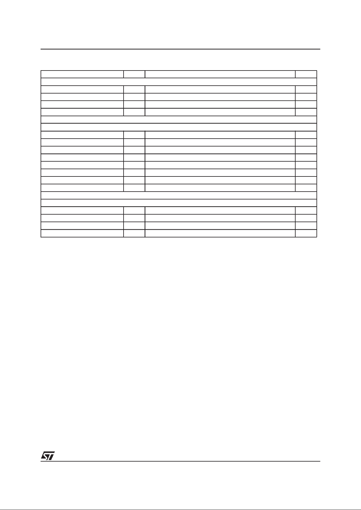
Table 2.1. Signal Description
Group name Qty
System Clocks & Resets 11
Memory Interface 95
PCI interface 60
ISA 79
89IDE 34
Local Bus 49
Video Input 11
TV Output 8
VGA Monitor interface 8
Grounds 71
V
DD
29
Analog specific V
CC/VDD
6
Total Pin Count 388
Figure 2.1. STPC Consumer-S External Interfaces
PCI
x86
SDRAM VGA VIP TV SYS ISA/IDE/LB
95 8 11 8 60 11 89
STPC CONSUMER-S
Page 11

PIN DESCRIPTION
11/51
Release B
This is preliminary information on a new product now in development or undergoing evaluation. Details are subject to change without notice.
Table 2.2. Definition of Signal Pins
Signal Name Dir Description Qty
BASIC CLOCKS AND RESETS
SYSRSTI# I System Power Good Input 1
SYSRSTO# O System Reset Output 1
XTALI I 14.3MHz Crystal Input 1
XTALO I/O 14.3MHz Crystal Output - External Oscillator Input 1
HCLK I/O Host Clock (Test) 1
DEV_CLK O 24MHz Peripheral Clock (floppy drive) 1
DCLK I/O 27-135MHz Graphics Dot Clock 1
MEMORY INTERFACE
MCLKI I Memory Clock Input 1
MCLKO O Memory Clock Output 1
CS#[3:0] O DIMM Chip Select 4
MA[11:0] O Memory Row & Column Address 12
MD[63:0] I/O Memory Data 64
RAS#[1:0] O Row Address Strobe 2
CAS#[1:0] O Column Address Strobe 2
MWE# O Write Enable 1
DQM[7:0] O Data Input/Output Mask 8
PCI INTERFACE
PCI_CLKI I 33MHz PCI Input Clock 1
PCI_CLKO O 33MHz PCI Output Clock (from internal PLL) 1
AD[31:0] I/O PCI Address / Data 32
CBE#[3:0] I/O Bus Commands / Byte Enables 4
FRAME# I/O Cycle Frame 1
IRDY# I/O Initiator Ready 1
TRDY# I/O Target Ready 1
LOCK# I PCI Lock 1
DEVSEL# I/O Device Select 1
STOP# I/O Stop Transaction 1
PAR I/O Parity Signal Transactions 1
SERR# O System Error 1
PCIREQ#[2:0] I PCI Request 3
PCI_GNT#[2:0] O PCI Grant 3
PCI_INT[3:0] I PCI Interrupt Request 4
VDD5 I 5V Power Supply for PCI ESD protection 4
ISA CONTROL
ISA_CLK O ISA Clock Output - Multiplexer Select Line For IPC 1
ISA_CLK2X O ISA Clock x2 Output - Multiplexer Select Line For IPC 1
OSC14M O ISA bus synchronisation clock 1
LA[23:17] O Unlatched Address 7
SA[19:0] I/O Latched Address 20
SD[15:0] I/O Data Bus 16
ALE O Address Latch Enable 1
MEMR#, MEMW# I/O Memory Read and Memory Write 2
SMEMR#, SMEMW# O System Memory Read and Memory Write 2
Page 12
PIN DESCRIPTION
12/51
Release B
This is preliminary information on a new product now in development or undergoing evaluation. Details are subject to change without notice.
IOR#, IOW# I/O I/O Read and Write 2
MCS16#, IOCS16# I Memory/IO Chip Select16 2
BHE# O System Bus High Enable 1
ZWS# I Zero Wait State 1
REF# O Refresh Cycle. 1
MASTER# I Add On Card Owns Bus 1
AEN O Address Enable 1
IOCHCK# I I/O Channel Check. 1
IOCHRDY I/O I/O Channel Ready (ISA) - Busy/Ready (IDE) 1
ISAOE# O ISA/IDE Selection 1
GPIOCS# I/O General Purpose Chip Select 1
IRQ_MUX[3:0] I Time-Multiplexed Interrupt Request 4
DREQ_MUX[1:0] I Time-Multiplexed DMA Request 2
DACK_ENC[2:0] O Encoded DMA Acknowledge 3
TC O ISA Terminal Count 1
RTCAS O Real Time Clock Address Strobe 1
RMRTCCS# I/O ROM/RTC Chip Select 1
KBCS# I/O Keyboard Chip Select 1
RTCRW# I/O RTC Read/Write 1
RTCDS I/O RTC Data Strobe 1
LOCAL BUS
PA[21:0] O Address Bus 22
PD[15:0] I/O Data Bus 16
PRD1#,PRD0# O Peripheral Read Control 2
PWR1#,PWR0# O Peripheral Write Control 2
PRDY# I Data Ready 1
FCS1#, FCS0# O Flash Chip Select 2
IOCS#[3:0] O I/O Chip Select 4
IDE CONTROL
DA[2:0] O Address Bus 3
DD[15:0] I/O Data Bus 16
PCS3#,PCS1#,SCS3#,SCS1# O Primary &Secondary Chip Selects 4
DIORDY O Data I/O Ready 1
PIRQ, SIRQ I Primary & Secondary Interrupt Request 2
PDRQ, SDRQ I Primary &Secondary DMA Request 2
PDACK#, SDACK# O Primary &Secondary DMA Acknowledge 2
PDIOR#, SDIOR# O Primary &Secondary I/O Channel Read 2
PDIOW#, SDIOW# O Primary &Secondary I/O Channel Write 2
MONITOR INTERFACE
RED, GREEN, BLUE O Analog Red, Green, Blue 3
VSYNC O Vertical Sync 1
HSYNC O Horizontal Sync 1
VREF_DAC I DAC Voltage reference 1
RSET I Resistor Set 1
COMP I Compensation 1
Table 2.2. Definition of Signal Pins
Signal Name Dir Description Qty
Page 13
PIN DESCRIPTION
13/51
Release B
This is preliminary information on a new product now in development or undergoing evaluation. Details are subject to change without notice.
2.2 SIGNAL DESCRIPTIONS
2.2.1 BASIC CLOCKS AND RESETS
SYSRSTI#
System Reset/Power good.
This input
is low when the reset switch is depressed. Otherwise, it reflects the power supply’s power good
signal. This input is asynchronous to all clocks,
and acts as anegative active reset. The reset circuit initiates a hard reset on the rising edge of this
signal.
SYSRSTO#
Reset Output to System.
This is the
system reset signaland is usedto reset therest of
the components (not on Host bus) in the system.
The ISA bus reset is an externally inverted buffered version of this outputand thePCI bus reset is
an externally buffered version of this output.
XTALI
14.3MHz Crystal Input
XTALO
14.3MHz Crystal Output.
These pins are
connected to the 14.318 MHz crystal to provide
the reference clock for the internal frequency synthesizer to generate all the other clocks.
A 14.318 MHz Series Cut Crystal should be connected between these two pins. Balance capacitors of 15 pF should alsobe added. In the eventof
an external quarzt oscillator providing the master
clock signal to the STPC Consumer-S device, the
TTL signal should be provided on XTALO.
HCLK
Host Clock.
This clock supplies the CPU
and the host related blocks. This clock can e doubled inside the CPU and is intended to operate in
the range of25 to 100 MHz. Thisclock in generated internally from a PLL but can be driven directly
from the external system.
DCLK
Dot Clock / Pixelclock.
This clock supplies
the display controller, the video pipeline, the ramdac, and the TV output logic. Its value is dependent on the selected display mode.
Its frequencycan be as high as 135MHz. Thissignal is either driven by the internal PLL either byan
external oscillator. The direction can be controlled
by a strap option oran internal register bit.
DEV_CLK
24MHz Peripheral Clock.
This 24MHZ
signal is provided asa convenience for thesystem
integration of a Floppy Disk driver function in an
external chip.
VIDEO INPUT
VCLK I 27-33MHz Video Input Port Clock 1
VIN I CCIR 601 or 656 YUV Video Data Input 8
VCS I/O Composite Synch orHorizontal line SYNC output 1
ODD_EVEN I/O Frame Synchronisation 1
ANALOG TV OUTPUT
RED_TV, GREEN_TV, BLUE_TV O Analog RGB or S-VHS outputs 3
CVBS O Analog video composite output 1
IREF1_TV I Reference current of 9bit DAC for CVBS 1
VREF1_TV I Reference voltage of 9bit DAC for CVBS 1
IREF2_TV I Reference current of 8bit DAC for R,G,B 1
VREF2_TV I Reference voltage of 8bit DAC for R,G,B 1
VSSA_TV I Analog Vss for DAC 1
VDDA_TV I Analog Vdd for DAC 1
MISCELLANEOUS
SPKRD O Speaker Device Output 1
SCL I/O I C Interface - Clock / Can be used for VG A D DC[1] signal 1
SDA I/O I C Interface - Data /Can be used for VGA DDC[0] signal 1
SCAN_ENAB LE I Reserved (Te st pin) 1
Table 2.2. Definition of Signal Pins
Signa l Name Dir Description Qty
Page 14

PIN DESCRIPTION
14/51
Release B
This is preliminary information on a new product now in development or undergoing evaluation. Details are subject to change without notice.
2.2.2 MEMORY INTERFACE
MCLKO
Memory Clock Output.
This clock is driving the DIMMs on board and is generated from an
internal PLL. The default value is 66MHz.
MCLKI
Memory Clock Input.
This clock is driving
the SDRAM controller, the graphics engine and
display controller. This input should be a buffered
version ofthe MCLKOsignal with the track lengths
between the buffer and the pin matched with the
track lengths between the buffer and the DIMMs.
CS#[3:0]
Chip Select
These signals are used to
disable or enable device operation by masking or
enabling all SDRAM inputs except MCLK, CKE,
and DQM.
MA[11:0]
Memory Address.
Multiplexed row and
column address lines.
MD[63:0]
Memory Data.
This is the 64-bit memory
data bus. MD[40-0] are read by the device strap
option registers during rising edge of SYSRSTI#.
RAS#[1:0]
Row Address Strobe.
These signals
enable row access and precharge. Row address
is latched on rising edge of MCLK when RAS# is
low.
CAS#[1:0]
Column Address Strobe.
These signals enable column access. Column address is
latched on rising edge of MCLK when CAS# is
low.
MWE#
Write Enable.
Write enable specifies
whether thememory accessis a read(MWE# =H)
or a write (MWE# = L).
DQM#[7:0]
Data Mask.
Makes data output Hi-Z
after the clock and masks the SDRAM outputs.
Blocks SDRAM data input when DQM active.
2.2.3 PCI INTERFACE
PCI_CLKI
33MHz PCI Input Clock.
This signal is
the PCI bus clock inputand shouldbe driven from
the PCI_CLKO pin.
PCI_CLKO
33MHz PCI Output Clock.
This is the
master PCI bus clock output.
AD[31:0]
PCI Address/Data.
This is the 32-bit
multiplexed address and databus of the PCI. This
bus is driven by the master during the address
phase and data phase of write transactions. It is
driven by the target during data phase of read
transactions.
CBE#[3:0]
Bus Commands/Byte Enables.
These
are the multiplexed command and byte enable
signals of the PCI bus. During the address phase
they define the command and during the data
phase they carry the byte enable information.
These pins are inputs when a PCI master other
than the STPC Consumer-S owns the bus and
outputs when the STPC Consumer-S owns the
bus.
FRAME#
Cycle Frame.
This is the frame signal of
the PCI bus. It is an input whenaPCI master owns
the bus and is an output when STPC Consumer-S
owns the PCI bus.
IRDY#
Initiator Ready.
This is the initiator ready
signal of thePCI bus. It is used as an output when
the STPCConsumer-S initiates a bus cycle on the
PCI bus. It is used as an input during the PCI cycles targeted to the STPC Consumer-S to determine when the current PCI master is ready to
complete the current transaction.
TRDY#
Target Ready.
This isthe target ready signal of the PCI bus. It is driven as an output when
the STPC Consumer-S is the target of thecurrent
bus transaction. Itis used as an input when STPC
Consumer-S initiates a cycle on the PCI bus.
LOCK#
PCI Lock.
This isthe lock signal of the PCI
bus and is used to implement the exclusive bus
operations when acting as a PCI target agent.
Page 15

PIN DESCRIPTION
15/51
Release B
This is preliminary information on a new product now in development or undergoing evaluation. Details are subject to change without notice.
DEVSEL#
I/O Device Select.
This signal is used
as an input when the STPC Consumer-S initiates
a bus cycle on the PCI bus to determine if a PCI
slave device has decoded itself to be the target of
the current transaction. It is asserted as anoutput
either whenthe STPC Consumer-S isthe targetof
the current PCI transaction or when no other device asserts DEVSEL# prior to the subtractive decode phase of the current PCI transaction.
STOP#
Stop Transaction.
Stop is used to implement the disconnect, retry and abort protocol of
the PCI bus. It is used as an input for the bus cycles initiated by the STPC Consumer-S and is
used as an output when a PCImaster cycle is targeted to the STPC Consumer-S.
PAR
Parity Signal Transactions.
This is the parity
signal of the PCI bus. This signal is used to guarantee even parity across AD[31:0], CBE#[3:0],
and PAR. This signal is driven by the master during the address phase and data phase of write
transactions. It is driven by the target during data
phase of read transactions. (Its assertion is identical to thatof theAD busdelayed by one PCI clock
cycle)
SERR#
System Error.
This isthe system errorsignal of the PCIbus. It may, if enabled, be asserted
for one PCI clock cycle if target aborts a STPC
Consumer-S initiated PCI transaction. Its assertion byeither theSTPC Consumer-S orby another
PCI bus agent will trigger the assertion of NMI to
the host CPU. This is an open drain output.
PCIREQ#[2:0]
PCI Request.
This pin are the
three external PCI master request pins. Theyindicates to the PCI arbiter that the external agents
desire use of the bus.
PCI_GNT#[2:0]
PCI Grant.
These pins indicate
that the PCI bus has been granted to the master
requesting it on its PCIREQ#.
PCI_INT[3:0]
PCI Interrupt Request.
These are
the PCI bus interrupt signals.
VDD5
5V Power Supply.
These power pins are
necessary for 5V ESD protection. In case the PCI
bus is used in 3.3V only, these pins can be connected to 3.3V.
2.2.4 ISA INTERFACE
ISA_CLK, ISA_CLKX2
ISA Clock x1, x2.
These
pins generatethe Clock signal forthe ISA bus and
a Doubled Clock signal. They arealso usedas the
multiplexor controllines for the Interrupt Controller
Interrupt input lines. ISA_CLK is generated from
either PCICLK/4 or OSC14M/ 2.
OSC14M
ISA bus synchronisation clock Output.
This is the buffered 14.318 Mhz clock for the ISA
bus.
LA[23:17]
Unlatched Address.
When the ISA bus
is active, these pins are ISA Bus unlatched address for 16-bit devices. When ISA bus is accessed by any cycle initiated from PCI bus, these
pins are in output mode. When an ISA bus master
owns the bus, these pins are in input mode.
SA[19:0]
ISA Address Bus.
System address bus
of ISA on 8-bit slot. These pins are usedas an input when an ISA bus master ownsthe busand are
outputs at all other times.
SD[15:0]
I/O Data Bus.
These pins are the exter-
nal databus to the ISA bus.
ALE
Address Latch Enable.
This is the address
latch enable output of the ISA bus and is asserted
by the STPC Consumer-S to indicate that LA2317, SA19-0, AEN and SBHE# signals are valid.
The ALE is driven high during refresh, DMA master oran ISA master cycles by theSTPC Consumer-S. ALE is driven low after reset.
MEMR#
Memory Read.
This is the memory read
command signal of theISA bus. It is used as an input when an ISA master owns the bus and is an
output at all other times.
The MEMR# signal is active during refresh.
MEMW#
Memory Write.
This is the memory write
command signal of theISA bus. It is used as an input when an ISA master owns the bus and is an
output at all other times.
SMEMR#
System Memory Read.
The STPC Consumer-S generates SMEMR# signal of the ISA
bus only whenthe addressis below onemegabyte
or the cycle is a refresh cycle.
Page 16

PIN DESCRIPTION
16/51
Release B
This is preliminary information on a new product now in development or undergoing evaluation. Details are subject to change without notice.
SMEMW#
System Memory Write.
The STPC Consumer-S generates SMEMW# signal of the ISA
bus only when the address is below one megabyte.
IOR#
I/O Read.
This is the IO read command signal of the ISAbus. Itis aninput when anISA master owns the bus and is an output at all other
times.
IOW#
I/O Write.
This is the IO write command signal of the ISAbus. Itis aninput when anISA master owns the bus and is an output at all other
times.
MCS16#
Memory Chip Select16.
This is the decode of LA23-17 address pins of the ISA address
bus without any qualification of the command signal lines. MCS16# is always an input. The STPC
Consumer-S ignores this signal during IO and refresh cycles.
IOCS16#
IO Chip Select16.
This signal is the decode of SA15-0 address pins of the ISA address
bus without any qualification of the command signals. The STPC Consumer-S does not drive
IOCS16# (similar to PC-AT design). An ISA master accessto an internal registerof the STPCConsumer-S is executed as an extended 8-bit IO cycle.
BHE#
System Bus HighEnable.
This signal, when
asserted, indicates that a data byte is being transferred onSD15-8 lines. Itis used asan inputwhen
an ISA master owns the bus andis an output at all
other times.
ZWS#
Zero Wait State.
This signal, when asserted by addressed device, indicates that current cycle can be shortened.
REF#
Refresh Cycle.
This isthe refresh command
signal of the ISA bus. It is driven as an output
when the STPC Consumer-S performs a refresh
cycle on the ISA bus. It is used as an input when
an ISA master owns thebus andis used to trigger
a refresh cycle.
The STPC Consumer-S performs a pseudo hidden refresh. It requests the host bus for two host
clocks to drive the refresh address and capture it
in external buffers. The host bus is then relinquished while the refresh cycle continues on the
ISA bus.
MASTER#
Add On Card Owns Bus.
This signal is
active when an ISA device has been granted bus
ownership.
AEN
Address Enable.
Address Enable is enabled
when the DMA controller is the bus owner to indicate that a DMA transfer will occur. The enabling
of the signal indicates to IO devices to ignore the
IOR#/IOW# signal during DMA transfers.
IOCHCK#
IO Channel Check.
IO Channel Check
is enabled by any ISA device to signal an error
condition thatcan not be corrected. NMI signal becomes active upon seeing IOCHCK# active if the
corresponding bit in Port B is enabled.
IOCHRDY
Channel Ready.
IOCHRDY is the IO
channel ready signal of the ISA bus and is driven
as an output in response to an ISA master cycle
targeted to the host bus or an internal register of
the STPC Consumer-S. The STPC Consumer-S
monitors this signal as an input when performing
an ISA cycle on behalf of the host CPU, DMA
master or refresh.
ISA masters which do not monitor IOCHRDY are
not guaranteed to work with the STPCConsumerS since the access to the system memory can be
considerably delayed due UMA architecture.
ISAOE#
Bidirectional OE Control.
This signal controls the OE signal of the external transceiver that
connects the IDE DD bus and ISA SA bus.
GPIOCS#
I/O General Purpose Chip Select.
This
output signal is used by the external latch on ISA
bus to latch the dataon the SD[7:0] bus. The latch
can be useby PMU unit tocontrol the externalperipheral devices or any other desired function.
IRQ_MUX[3:0]
Multiplexed Interrupt Request.
These are the ISA bus interrupt signals. They
have to be encoded before connection to the
STPC Consumer-Susing ISACLKand ISACLKX2
as the input selection strobes.
Note that IRQ8B, which by conventionis connected to the RTC,is inverted before being sentto the
interrupt controller, so that it maybe connected directly to the IRQ pin of the RTC.
DREQ_MUX[1:0]
ISA Bus Multiplexed DMA Re-
quest.
These are the ISA bus DMA request signals. Theyare to be encoded beforeconnection to
the STPC Consumer-S using ISACLK and
ISACLKX2 as the input selection strobes.
Page 17

PIN DESCRIPTION
17/51
Release B
This is preliminary information on a new product now in development or undergoing evaluation. Details are subject to change without notice.
DACK_ENC[2:0]
DMA Acknowledge.
These are
the ISA bus DMA acknowledge signals. They are
encoded by the STPC Consumer-S before output
and should be decoded externally using ISACLK
and ISACLKX2 as the control strobes.
TC
ISA Terminal Count.
This is the terminal count
output of the DMA controller and is connected to
the TCline of the ISA bus. It isasserted during the
last DMA transfer, when the byte count expires.
2.2.5 X-Bus Interface pins
RTCAS#
Real timeclock address strobe.
This sig-
nal is asserted for any I/O write to port 70H.
RMRTCCS#
ROM/Real Time clock chip select.
This signal is asserted if a ROM access is decoded during a memory cycle. It should be combined
with MEMR# or MEMW# signals to properly access the ROM. During a IO cycle,this signal is asserted if access to the Real Time Clock (RTC) is
decoded. It shouldbe combined with IOR orIOW#
signals to properly access the real time clock.
KBCS#
Keyboard Chip Select.
This signal is asserted if a keyboard access is decoded during a I/
O cycle.
RTCRW#
Real TimeClock RW.
This pinis amultifunction pin. When ISAOE#is active, this signal is
used as RTCRW#. This signal is asserted for any
I/O write to port 71H.
RTCDS#
Real Time Clock DS
. This pin is a multifunction pin. When ISAOE#is active, this signal is
used as RTCDS. This signal is asserted for any I/
O read to port 71H.
Note: RMRTCCS#, KBCS#, RTCRW# and
RTCDS# signals must be ORed externally with
ISAOE# and then connected to the external device. An LS244 or equivalent function can be used
if OE# is connected to ISAOE# and the output is
provided with a weak pull-up resistor as shown in
Figure 2.2.
2.2.6 LOCAL BUS
PA[21:0]
Address Bus Output.
PD[15:0]
Data Bus.
This is the 16-bit data bus.
D[7:0] is the LSB and PD[15:8] is the MSB.
PWR#[1:0]
Write Control output.
PWR0# is used
to write the LSB and PWR1# to write the MSB.
PRD#[1:0]
Read Control output.
PRD0# is used
to read the LSB and PRD1# to read the MSB.
PRDY#
Data Ready input.
This signal is used to
create wait states on the bus. When low, it completes the current cycle.
FCS#[1:0]
Flash Chip Select output.
These are
the Programmable Chip Select signals for up to 2
banks of Flash memory.
IOCS#[3:0]
I/O ChipSelect output.
These are the
Programmable Chip Select signals for up to 4 external I/O devices.
Page 18

PIN DESCRIPTION
18/51
Release B
This is preliminary information on a new product now in development or undergoing evaluation. Details are subject to change without notice.
2.2.7 IDE INTERFACE
PCS1#, PCS3#
Primary Chip Select.
These signals are used as the active high primary master &
slave IDE chip select signals. These signals must
be externally ANDed with the ISAOE# signal before driving the IDE devices to guarantee it is active only when ISA bus is idle.
SCS1#, SCS3#
Secondary Chip Select.
These
signals are used as the active high secondary
master & slave IDE chip select signals. These signals must be externally ANDed with the ISAOE#
signal before driving theIDE devices to guarantee
it is active only when ISA bus is idle.
DA[2:0]
Address.
These signals are connected to
DA[2:0] ofIDE devices directly or through abuffer.
If the toggling of signals are to be masked during
ISA bus cycles, they can be externally ORed with
ISAOE# before being connected to the IDE devices.
DD[15:0]
Databus.
When the IDE bus is active,
they serve as IDE signals DD[11:0]. IDE devices
are connected to SA[19:8] directly and ISA bus is
connected to these pins throughtwo LS245 transceivers as described in Figure 2.2.
DIORDY
Busy/Ready.
This pin serves as IDE sig-
nal DIORDY.
PIRQ
Primary Interrupt Request.
SIRQ
Secondary Interrupt Request.
Interrupt request from IDE channels.
PDRQ
Primary DMA Request.
SDRQ
Secondary DMA Request.
DMA request from IDE channels.
PDACK#
Primary DMA Acknowledge.
SDACK#
Secondary DMA Acknowledge.
DMA acknoledge to IDE channels.
PDIOR#, PDIOW#
Primary I/O Read &Write.
SDIOR#, SDIOW#
Secondary I/ORead & Write
.
Primary & Secondary channel read & write.
2.2.8 Monitor Interface
RED, GREEN, BLUE
RGB Video Outputs.
These
are the3 analog color outputs from the RAMDACs
VSYNC
Vertical Synchronisation Pulse.
This is
the vertical synchronization signal from the VGA
controller.
HSYNC
Horizontal Synchronisation Pulse.
This is
the horizontal synchronization signal from the
VGA controller.
VREF_DAC
DAC Voltage reference.
An external
voltage reference is connected to this pin to bias
the DAC.
RSET
Resistor Current Set.
This reference current input to the RAMDAC is used to set the fullscale output of the RAMDAC.
COMP
Compensation.
This is the RAMDAC compensation pin. Normally, an external capacitor
(typically 10nF) is connected between this pin and
VDDto damp oscillations.
Page 19

PIN DESCRIPTION
19/51
Release B
This is preliminary information on a new product now in development or undergoing evaluation. Details are subject to change without notice.
2.2.9 VIDEO INTERFACE
VCLK
Pixel Clock Input.
This signal is used tosynchronise data being transfered from an external
video device toeither the frame buffer, or alternatively out the TV output in bypass mode. This pin
can be sourced from STPC if no external VCLK is
detected, or can be input from an external video
clock source.
VIN[7:0]
YUV Video Data Input CCIR 601 or 656.
Time multiplexed 4:2:2 luminance and chrominance data as defined in ITU-R Rec601-2 and
Rec656 (except for TTL input levels). This bus
typically carries a stream of Cb,Y,Cr,Y digital video at VCLK frequency, clocked on the rising edge
(by default) of VCLK.
VCS
Line synchronisation Output.
This pin is an
input in ODDEV+HSYNC or VSYNC + HSYNC or
VSYNC slave modes and an output in all other
modes (master/slave)
ODD_EVEN
Frame Synchronisation Ourput.
This
pin supports the Frame synchronisation signal. It
is an input in slave modes, except when sync is
extracted from YCrCbdata, and an output in master mode and when sync is extracted from YCrCb
data
The signal is synchronous to rising edge ofDCLK.
The default polarity for this pin is:
- odd (not-top) field : LOW level
- even (bottom) field : HIGH level
2.2.10 TV OUTPUT
RED_TV / C_TV
Analog video outputs synchro-
nized withCVBS.
This outputis current-drivenand
must be connected to analog ground over a load
resistor (R
LOAD
). Following the load resistor, a
simple analog low pass filter is recommended. In
S-VHS mode, this is the Chrominance Output.
GREEN_TV / Y_TV
Analog video outputs syn-
chronized with CVBS.
This output is current-driven and must be connected to analog ground over
a load resistor (R
LOAD
). Following the load resistor, a simple analog low pass filter is recommended. In S-VHS mode, this is the Luminance Output.
BLUE_TV / CVBS
Analog video outputs synchro-
nized withCVBS.
This outputis current-drivenand
must be connected to analog ground over a load
resistor (R
LOAD
). Following the load resistor, a
simple analog low pass filter is recommended. In
S-VHS mode, this is a second composite output.
CVBS
Analog videocomposite output (luminance/
chrominance).
CVBS is current-driven and must
be connected to analog ground over a load resistor (R
LOAD
). Following the load resistor, a simple
analog low pass filter is recommended.
IREF1_TV
Ref. current
for CVBS 10-bit DAC.
IREF2_TV
Reference current
for RGB 9-bit DAC.
VREF1_TV
Ref. voltage
for CVBS 10-bit DAC.
VREF2_TV
Reference voltage
for RGB9-bit DAC.
VSSA_TV
Analog V
SS
for DACs.
VDDA_TV
Analog V
DD
for DACs.
Page 20

PIN DESCRIPTION
20/51
Release B
This is preliminary information on a new product now in development or undergoing evaluation. Details are subject to change without notice.
2.2.11 MISCELLANEOUS
SPKRD
Speaker Drive.
This the output to the
speaker and is AND of the counter 2 output with
bit 1 of Port 61, and drives an external speaker
driver. This output should be connected to 7407
type high voltage driver.
SCL, SDA I C Interface.These bidirectional pins
are connected to CRTC register 3Fh to implement
DDC capabilities. They conform to I2C electrical
specifications, t hey have open-collector output
drivers which are internally connected to V
DD
through pull-up resistors.
They can be used for the DDC1 (SCL) and DDC0
(SDA) lines of the VGA interface.
SCAN_ENABLE
Reserved
. T he pin is res erved
for Test and Miscellaneous functions.
Page 21

PIN DESCRIPTION
21/51
Release B
This is preliminary information on a new product now in development or undergoing evaluation. Details are subject to change without notice.
Table 2.3. ISA / IDE dynamic multiplexing
.
Table 2.4. ISA / Local Bus pin sharing
.
ISABUS
(ISAOE# = 0)
IDE
(ISAOE# = 1)
RMRTCCS# DD[15]
KBCS# DD[14]
RTCRW# DD[13]
RTCDS DD[12]
SA[19:8] DD[11:0]
LA[23] SCS3#
LA[22] SCS1#
SA[21] PCS3#
SA[20] PCS1#
LA[19:17] DA[2:0]
IOCHRDY DIORDY
ISA / IPC LOCAL BUS
SD[15:0] PD[15:0]
DREQ_MUX[1:0] PA[21:20]
SMEMR# PA[19]
MEMW# PA[18]
BHE# PA[17]
AEN PA[16]
ALE PA[15]
MEMR# PA[14]
IOR# PA[13]
IOW# PA[12]
REF# PA[11]
IOCHCK# PA[10]
GPIOCS# PA[9]
ZWS# PA[8]
SA[7:4] PA[7:4]
TC, DACK_ENC[2:0] PA[3:0]
SA[3] PRDY
ISAOE#,SA[2:0] IOCS#[3:0]
DEV_CLK, RTCAS# FCS#[1:0]
IOCS16#, MASTER# PRD#[1:0]
SMEMW#, MCS16# PWR#[1:0]
ISACLK, ISA_CLK2X
Figure 2.2. Typical ISA/IDE Demultiplexing
MASTER#
74LS245
RMRTCCS#
AB
DIR
OEISAOE#
KBCS#
RTCRW#
RTCDS
SA[19:8]
STPC bus / DD[15:0]
LA[22]
LA[23]
LA[22]
LA[23]
SCS1#
SCS3#
PCS1#
PCS3#
Page 22

PIN DESCRIPTION
22/51
Release B
This is preliminary information on a new product now in development or undergoing evaluation. Details are subject to change without notice.
Table 2.5. Pinout.
Pin # Pin name
AF3 SYSRSTI#
AE4 SYSRSTO#
A3 XTALI
C4 XTALO
G23 HCLK
H24 DEV_CLK
AD11 DCLK
AF15 MCLKI
AB23 MCLKO
AE16 MA[0]
AD15 MA[1]
AF16 MA[2]
AE17 MA[3]
AD16 MA[4]
AF17 MA[5]
AE18 MA[6]
AD17 MA[7]
AF18 MA[8]
AE19 MA[9]
AE20 MA[10]
AC19 MA[11]
AF22 CS#[0]
AD21 CS#[1]
AE24 CS#[2]
AD23 CS#[3]
AF23 RAS#[0]
AD22 RAS#[1]
AE21 CAS#[0]
AC20 CAS#[1]
AF20 DQM#[0]
AD19 DQM#[1]
AF21 DQM#[2]
AD20 DQM#[3]
AE22 DQM#[4]
AE23 DQM#[5]
AF19 DQM#[6]
AD18 DQM#[7]
AC22 MWE#
R1 MD[0]
T2 MD[1]
R3 MD[2]
T1 MD[3]
R4 MD[4]
U2 MD[5]
T3 MD[6]
U1 MD[7]
U4 MD[8]
V2 MD[9]
U3 MD[10]
V1 MD[11]
W2 MD[12]
V3 MD[13]
Y2 MD[14]
W4 MD[15]
Y1 MD[16]
W3 MD[17]
AA2 MD[18]
Y4 MD[19]
AA1 MD[20]
Y3 MD[21]
AB2 MD[22]
AB1 MD[23]
AA3 MD[24]
AB4 MD[25]
AC1 MD[26]
AB3 MD[27]
AD2 MD[28]
AC3 MD[29]
AD1 MD[30]
AF2 MD[31]
AF24 MD[32]
AE26 MD[33]
AD25 MD[34]
AD26 MD[35]
AC25 MD[36]
AC24 MD[37]
AC26 MD[38]
AB25 MD[39]
AB24 MD[40]
AB26 MD[41]
AA25 MD[42]
Y23 MD[43]
AA24 MD[44]
AA26 MD[45]
Y25 MD[46]
Y26 MD[47]
Y24 MD[48]
W25 MD[49]
V23 MD[50]
W26 MD[51]
W24 MD[52]
V25 MD[53]
V26 MD[54]
U25 MD[55]
V24 MD[56]
U26 MD[57]
U23 MD[58]
Pin # Pin name
T25 MD[59]
U24 MD[60]
T26 MD[61]
R25 MD[62]
R26 MD[63]
F24 PCI_CLKI
D25 PCI_CLKO
B20 AD[0]
C20 AD[1]
B19 AD[2]
A19 AD[3]
C19 AD[4]
B18 AD[5]
A18 AD[6]
B17 AD[7]
C18 AD[8]
A17 AD[9]
D17 AD[10]
B16 AD[11]
C17 AD[12]
B15 AD[13]
A15 AD[14]
C16 AD[15]
B14 AD[16]
D15 AD[17]
A14 AD[18]
B13 AD[19]
D13 AD[20]
A13 AD[21]
C14 AD[22]
B12 AD[23]
C13 AD[24]
A12 AD[25]
C12 AD[26]
A11 AD[27]
D12 AD[28]
B10 AD[29]
C11 AD[30]
A10 AD[31]
D10 CBE[0]
C10 CBE[1]
A9 CBE[2]
B8 CBE[3]
A8 FRAME#
B7 TRDY#
D8 IRDY#
A7 STOP#
C8 DEVSEL#
B6 PAR
Pin # Pin name
Page 23

PIN DESCRIPTION
23/51
Release B
This is preliminary information on a new product now in development or undergoing evaluation. Details are subject to change without notice.
D7 SERR#
A6 LOCK#
D20 PCI_REQ#[0]
C21 PCI_REQ#[1]
A21 PCI_REQ#[2]
C22 PCI_GNT#[0]
A22 PCI_GNT#[1]
B21 PCI_GNT#[2]
A5 PCI_INT[0]
C6 PCI_INT[1]
B4 PCI_INT[2]
D5 PCI_INT[3]
A16 VDD5
B11 VDD5
B9 VDD5
D18 VDD5
F2 LA[17]/DA[0]
G4 LA[18]/DA[1]
F3 LA[19]/DA[2]
F1 LA[20]/PCS1#
G2 LA[21]/PCS3#
G1 LA[22]/SCS1#
H2 LA[23]/SCS3#
J4 SA[0]
H1 SA[1]
H3 SA[2]
J2 SA[3]
J1 SA[4]
K2 SA[5]
J3 SA[6]
K1 SA[7]
K4 SA[8]
L2 SA[9]
K3 SA[10]
L1 SA[11]
M2 SA[12]
M1 SA[13]
L3 SA[14]
N2 SA[15]
M4 SA[16]
M3 SA[17]
P2 SA[18]
P4 SA[19]
K25 SD[0]
L24 SD[1]
K26 SD[2]
K23 SD[3]
J25 SD[4]
Pin # Pin name
K24 SD[5]
J26 SD[6]
H25 SD[7]
H26 SD[8]
J24 SD[9]
G25 SD[10]
H23 SD[11]
D24 SD[12]
C26 SD[13]
A25 SD[14]
B24 SD[15]
AD4 ISA_CLK
AF4 ISA_CLK2X
C9 OSC14M
P25 ALE
AE8 ZWS#
R23 BHE#
P26 MEMR#
R24 MEMW#
N25 SMEMR#
N23 SMEMW#
N26 IOR#
P24 IOW#
N24 MCS16#
M26 IOCS16#
M25 MASTER#
L25 REF#
M24 AEN
L26 IOCHCK#
T24 IOCHRDY
M23 ISAOE#
A4 RTCAS#
P3 RTCDS#
R2 RTCRW#
P1 RMRTCCS#
AE3 GPIOCS#
E23 IRQ_MUX[0]
D26 IRQ_MUX[1]
E24 IRQ_MUX[2]
C25 IRQ_MUX[3]
A24 DREQ_MUX[0]
B23 DREQ_MUX[1]
C23 DACK_ENC[0]
A23 DACK_ENC[1]
B22 DACK_ENC[2]
D22 TC
C5 SPKRD
N3 KBCS#
Pin # Pin name
B1 PIRQ
C2 SIRQ
C1 PDRQ
D2 SDRQ
D3 PDACK#
D1 SDACK#
E2 PDIOR#
E4 PDIOW#
E3 SDIOR#
E1 SDIOW#
AF9 RED
AE9 GREEN
AD8 BLUE
AC5 VSYNC
AE5 HSYNC
AC10 VREF_DAC
AE10 RSET
AD7 COMP
B5 SCL
C7 SDA
AE15 VCLK
AD5 VIN[0]
AF7 VIN[1]
AF5 VIN[2]
AE6 VIN[3]
AC7 VIN[4]
AD6 VIN[5]
AF6 VIN[6]
AE7 VIN[7]
AD10 RED_TV
AF11 GREEN_TV
AE12 BLUE_TV
AE13 VCS
AC12 ODD_EVEN
AF14 CVBS
AE11 IREF1_TV
AF12 VREF1_TV
AE14 IREF2_TV
AC14 VREF2_TV
AD12 VDDA_TV
AF8 VDD_DAC1
AD9 VDD_DAC2
AF13 VSSA_TV
AC9 VSS_DAC1
AF10 VSS_DAC2
Pin # Pin name
Page 24

PIN DESCRIPTION
24/51
Release B
This is preliminary information on a new product now in development or undergoing evaluation. Details are subject to change without notice.
B3 SCAN_ENABLE
G24 VDD_CPUCLK_PLL
AD13 VDD_DCLK_PLL
F25 VDD_DEVCLK_PLL
AC17 VDD_MCLKI_PLL
AC15 VDD_MCLKO_PLL
F26 VDD_HCLK_PLL
A20 VDD
C15 VDD
D6 VDD
D11 VDD
D16 VDD
D21 VDD
F4 VDD
F23 VDD
G3 VDD
G26 VDD
L4 VDD
L23 VDD
N1 VDD
T4 VDD
T23 VDD
W1 VDD
AA4 VDD
AA23 VDD
AC6 VDD
AC2 VDD
AC11 VDD
AC16 VDD
AC21 VDD
E25 VSS_DLL
E26 VSS_DLL
A1:2 VSS
A26 VSS
B2 VSS
B25:26 VSS
C3 VSS
C24 VSS
D4 VSS
D9 VSS
D14 VSS
D19 VSS
D23 VSS
H4 VSS
J23 VSS
L11:16 VSS
M11:16 VSS
Pin # Pin name
N4 VSS
N11:16 VSS
P11:16 VSS
P23 VSS
R11:16 VSS
T11:16 VSS
V4 VSS
W23 VSS
AC4 VSS
AC8 VSS
AC13 VSS
AC18 VSS
AC23 VSS
AD3 VSS
AD14 VSS
AD24 VSS
AE1:2 VSS
AE25 VSS
AF1 VSS
AF25 VSS
AF26 VSS
Pin # Pin name
Page 25

STRAP OPTIONS
25/51
Release B
This ispreliminary information on a new product now in developement. Details are subject tochange without notice
3 STRAP OPTIONS
This chapter defines the STPC Consumer-S Strap Options and their location
Memory
Data
Lines
Note Refer to Designation Location
Actual
Settings
Set to ’0’ Set to ’1’
MD0 1 - Reserved - - - MD1 - Reserved - - - MD2 - Reserved - - - MD3 - Reserved - - - MD4 - Reserved - - - MD5 - Reserved - - - MD6 - Reserved - - - MD7 - Reserved - - - MD8 - Reserved - - - -
MD9 - Reserved - - - MD10 - Reserved - - - MD11 - Reserved - - - MD12 - Reserved - - - MD13 - Reserved - - - MD14 - Reserved - - - MD15 - Reserved - - - MD16 - Reserved Index 4C,bit0 Pull up - MD17 PCI Clock PCI_CLKO Divisor Index 4C,bit 1 User defined HCLK / 3 HCLK / 2
MD18 Reserved Index 4C,bit 2 Pull up - MD19 Reserved Index 4C,bit 3 Pull up
MD20 Reserved Index 4C, bit4 Pull up - MD21 Reserved Index 5F, bit 0 Pull up
MD22 Reserved Index 5F, bit 1 Pull up
MD23 - Reserved Index 5F,bit 2 Pull up - MD24 HCLK HCLK PLL Speed Index 5F,bit 3 User defined 000 25 MHz
MD25 Index 5F,bit 4 User defined 001 33 MHz
MD26 Index 5F,bit 5 User defined 010 100 MHz
011 50 MHz
100 60 MHz
101 66 MHz
110 75 MHz
111 90 MHz
MD27 Reserved Pull down
MD28 Reserved Pull down
MD29 Reserved Pull down
MD30 Reserved Pull down
MD31 Reserved Pull down
MD32 Reserved Pull down
MD33 Reserved Pull down
MD34 Reserved Pull down
MD35 Reserved Pull down
MD36 Reserved Pull up
MD37 Reserved Pull up
MD38 Reserved Pull up
Page 26

STRAP OPTIONS
26/51 Release 1.4
Release B
This ispreliminary information on a new product now in developement. Details are subject tochange without notice
Note;
1) This Strap Option selects between two different functional blocks, the first is the ISA and the other is
the VGA block.
3.1 STRAP REGISTER DESCRIPTION
Strap Option [16:0] are reserved.
3.1.1 STRAP REGISTER 2 INDEX 4CH (STRAP2)
Bits 4-0of this register reflect the status of pins MD[20:16] respectively. Bit 5 of this register reflectthe status of pin MD[23]. Bit 4 is writeable, writesto other bits in this registerhave no effect. Theyare useby the
chip as follows:
Bit 4-2; Reserved
Bit 1; This bit reflects the value sampled on MD[17] pin and controls the PCI clock output as follows:
0: PCI clock output = HCLK / 2
1: PCI clock output = HCLK / 3
Bit 0; Reserved
This register defaults to the values sampled on MD[23] & MD[20:16] pins after reset.
3.1.2 HCLK PLL STRAP REGISTER 0 INDEX 5FH (HCLK_Strap)
Bits 5-0 of this register reflect the status of pins MD[26:21] respectively.
They are use by the chip as follows:
Bits 5-3 These pins reflectthe value sampled on MD[26:24] pins respectively and control the Hostclock
frequency synthesizer.
Bit 2-0; Reserved
This register defaults to the values sampled on above pins after reset.
MD39 Reserved Pull up
MD40 CPU CPU Mode User defined DX1 DX2
MD41 Reserved Pull down
MD42 Reserved Pull down
MD43 Reserved Pull down
Memory
Data
Lines
Note Refer to Designation Location
Actual
Settings
Set to ’0’ Set to ’1’
Page 27

STRAP OPTIONS
27/51
Release B
This ispreliminary information on a new product now in developement. Details are subject tochange without notice
3.1.3 486 CLOCK PROGRAMMING (486_CLK)
The bit MD[40] is used to set the clock multiplication factorof the 486core. With the MD[40] pin pulled low
the 486 will run in DX (x1) mode, while with the MD[40] pin pulled high the 486 will run in DX2 (x2) mode.
The default value of the resistor on this strap input should be a resister to gnd (DX mode).
Strap Options [43:41] and [39:27] are reserved.
Page 28

ELECTRICAL SPECIFICATIONS
28/51
Release B
This is preliminary information on a new product now in development or undergoing evaluation. Details are subject to change without notice.
4 ELECTRICAL SPECIFICATIONS
4.1 Introduction
The electricalspecifications in this chapterare valid for the STPC Consumer-S.
4.2 Electrical Connections
4.2.1 Power/Ground Connections/Decoupling
Due to the high frequency of operation of the
STPC Consumer-S, it is necessary to install and
test this device using standard high frequency
techniques. The high clock frequencies used in
the STPC Consumer-S and its output buffer circuits can cause transientpower surges when several output buffers switch output levels simultaneously. These effects can be minimized by filtering
the DC power leads with low-inductance decoupling capacitors, using low impedance wiring, and
by utilizing all of the VSS and VDD pins.
4.2.2 Unused Input Pins
All inputs not used by the designer and not listed
in the table ofpin connections in Chapter 3should
be connected either to VDD or to VSS. Connect
active-high inputsto VDD through a20 kΩ (±10%)
pull-down resistor and active-low inputs to VSS
and connect active-low inputs to VCC through a
20 kΩ (±10%) pull-up resistor to prevent spurious
operation.
4.2.3 Reserved Designated Pins
Pins designated reserved should be left disconnected. Connecting a reserved pin to a pull-up resistor, pull-down resistor,or an active signal could
cause unexpected results and possible circuit
malfunctions.
4.3 Absolute Maximum Ratings
The following table lists the absolute maximum
ratings for the STPC Consumer-S device. Stresses beyond those listed under Table 4.1 limits may
cause permanent damage to the device. These
are stress ratings only and do not imply that operation under any conditions other than those specified in section ”Operating Conditions”.
Exposure to conditionsbeyond Table 4.1 may (1)
reduce device reliability and (2) result in premature failure evenwhen there is no immediately apparent sign offailure. Prolonged exposure to conditions at or near the absolute maximum ratings
(Table 4.1) may also result in reduced useful life
and reliability.
Table 4.1. Absolute Maximum Ratings
Symbol Parameter Value Units
V
DDx
DC Supply Voltage -0.3, 4.0 V
V
I,VO
Digital Input and Output Voltage -0.3, VDD + 0.3 V
T
STG
Storage Temperature -40, +150 °C
T
OPER
Operating Temperature 0, +70 °C
P
TOT
Total Power Dissipation 4.8 W
Page 29

ELECTRICAL SPECIFICATIONS
29/51
Release B
This is preliminary information on a new product now in development or undergoing evaluation. Details are subject to change without notice.
4.1 DC Characteristics
Notes:
1. MHz ratings refer to CPU clock frequency.
2. Not 100% tested.
4.1 AC Characteristics
Table 4.4 through Table 4.9 list the AC characteristics including output delays, input setup requirements, input hold requirements and output float
delays. These measurements are based on the
measurement points identified in Figure 4.1. The
rising clock edgereference level VREF , andother
reference levels are shown in Table 4.3 below for
the STPC Consumer-S. Input or output signals
must cross these levels during testing.
Figure 4.1 showsoutput delay (A andB) and input
setup and hold times (C and D). Input setup and
hold times (C and D) are specified minimums, defining the smallest acceptable sampling window a
synchronous input signal must be stable for correct operation.
Note: Refer to Figure 4.1.
Table 4.2. DC Characteristics
Recommended Operating conditions : VDD = 3.3V ±0.3V, Tcase = 0 to 100°C unless otherwise specified
Symbol Parameter Test conditions Min Typ Max Unit
V
DD
Operating Voltage 3.0 3.3 3.6 V
P
DD
Supply Power VDD= 3.3V, H
CLK
= 66Mhz 3.2 3.9 W
H
CLK
Internal Clock (Note 1) 75 Mhz
V
REF
DAC Voltage Reference 1.215 1.235 1.255 V
V
OL
Output Low Voltage I
Load
=1.5 to 8mA depending of the pin 0.5 V
V
OH
Output High Voltage I
Load
=-0.5 to -8mA depending of thepin 2.4 V
V
IL
Input Low Voltage Except XTALI -0.3 0.8 V
XTALI -0.3 0.9 V
V
IH
Input High Voltage Except XTALI 2.1 VDD+0.3 V
XTALI 2.35 V
DD
+0.3 V
I
LK
Input Leakage Current Input, I/O -5 5 µA
C
IN
Input Capacitance (Note 2) pF
C
OUT
Output Capacitance (Note 2) pF
C
CLK
Clock Capacitance (Note 2) pF
Table 4.3. Drive Level and Measurement Points for Switching Characteristics
Symbol Value Units
V
REF
1.5 V
V
IHD
3.0 V
V
ILD
0.0 V
Page 30

ELECTRICAL SPECIFICATIONS
30/51
Release B
This is preliminary information on a new product now in development or undergoing evaluation. Details are subject to change without notice.
Figure 4.1. Drive Level and Measurement Points for Switching Characteristics
CLK:
V
Ref
V
ILD
V
IHD
Tx
LEGEND: A - Maximum Output Delay Specification
B - Minimum Output Delay Specification
C - Minimum Input Setup Specification
D - Minimum Input Hold Specification
V
Ref
Va lid
Valid
Valid
OUTPUTS:
INPUTS:
Output n
Output n+1
Input
MAX
MIN
A
B
CD
V
Ref
V
ILD
V
IHD
Page 31

ELECTRICAL SPECIFICATIONS
31/51
Release B
This is preliminary information on a new product now in development or undergoing evaluation. Details are subject to change without notice.
Table 4.4. PCI Bus AC Timing
Name Parameter Min Max Unit
t1 PCI_CLKI to AD[31:0] valid 2 11 ns
t2 PCI_CLKI to FRAME# valid 2 11 ns
t3 PCI_CLKI to CBE#[3:0] valid 2 11 ns
t4 PCI_CLKI to PAR valid 2 11 ns
t5 PCI_CLKI to TRDY# valid 2 11 ns
T6 PCI_CLKI to IRDY# valid 2 11 ns
T7 PCI_CLKI to STOP# valid 2 11 ns
T8 PCI_CLKI to DEVSEL# valid 2 11 ns
T9 PCI_CLKI to PCI_GNT# valid 2 12 ns
t10 AD[31:0] bus setup to PCI_CLKI 7 ns
t11 AD[31:0] bus hold from PCI_CLKI 0 ns
t12 PCI_REQ#[2:0] setup to PCI_CLKI 10 ns
t13 PCI_REQ#[2:0] hold from PCI_CLKI 0 ns
t14 CBE#[3:0] setup to PCI_CLKI 7 ns
t15 CBE#[3:0] hold to PCI_CLKI 0 ns
t16 IRDY# setup to PCI_CLKI 7 ns
t17 IRDY# hold to PCI_CLKI 0 ns
t18 FRAME# setup to PCI_CLKI 7 ns
t19 FRAME# hold from PCI_CLKI 0 ns
Table 4.5. IDE Bus AC Timing
Name Parameter Min Max Unit
t20 DD[15:0] setup to PIOR#/SIOR# falling 15 ns
t21 DD[15:0} hold to PIOR#/SIOR# falling 12 ns
Table 4.6. SDRAM Bus AC Timing
Name Parameter Min Max Unit
ns
ns
ns
ns
ns
ns
ns
ns
ns
ns
ns
ns
Page 32

ELECTRICAL SPECIFICATIONS
32/51
Release B
This is preliminary information on a new product now in development or undergoing evaluation. Details are subject to change without notice.
Table 4.7. Video Input/TV Output AC Timing
Name Parameter Min Max Unit
t35 VIDEO_D[7:0] setup to VCLK 5 ns
t36 VIDEO_D[7:0] hold from VCLK 2 ns
t37 VCLK to VTV_BT# valid 15 ns
t38 VCLK to VTV_HSYNC valid 15 ns
t39 VTV_BT# setup to VCLK 10 ns
t40 VTV_BT# hold from VCLK 5 ns
t41 VTV_HSYNC setup to VCLK 10 ns
t42 VTV_HSYNC hold from VCLK 5 ns
Table 4.8. Graphics Adapter (VGA) AC Timing
Name Parameter Min Max Unit
t43 DCLK to VSYNC valid 45 ns
t44 DCLK to HSYNC valid 45 ns
Table 4.9. ISA Bus AC Timing
Name Parameter Min Max Unit
t45 XTALO to LA[23:17] bus active 60 ns
t46 XTALO to SA[19:0] bus active 60 ns
t47 XTALO to BHE# valid 62 ns
t48 XTALO to SD[15:0] bus active 35 ns
t49 PCI_CLKI to ISAOE# valid 28 ns
t50 XTALO to GPIOCS# valid 60 ns
t51 XTALO to ALE valid 62 ns
t52 XTALO to MEMW# valid 50 ns
t53 XTALO to MEMR# valid 50 ns
t54 XTALO to SMEMW# valid 50 ns
t55 XTALO to SMEMR# valid 50 ns
t56 XTALO to IOR# valid 50 ns
t57 XTALO to IOW# valid 50 ns
Page 33

MECHANICAL DATA
33/51
Release B
5. MECHANICAL DATA
5.1 388-PIN PACKAGE DIMENSION
The pin numbering for the STPC 388-pin Plastic
BGA package is shown in Figure 5-1.
Dimensions are shown in Figure 5-2, Table 5-1
and Figure 5-3, Table 5-2.
Figure 5-1. 388-Pin PBGA Package - Top View
A
B
D
E
F
G
H
J
K
L
M
N
P
R
T
U
V
W
Y
AA
AB
AC
AD
AE
AF
C
1 3 5 7 9 11 13 15 17 19 21 23 25
2468101214161820222426
A
B
D
E
F
G
H
J
K
L
M
N
P
R
T
U
V
W
Y
AA
AB
AC
AD
AE
AF
C
1 3 5 7 9 1113151719212325
2468101214161820222426
Page 34

MECHANICAL DATA
34/51
Release B
Figure 5-2. 388-pin PBGA Package - PCB Dimensions
Table 5-1. 388-pin PBGA Package - PCB Dimensions
Symbols
mm inches
Min Typ Max Min Typ Max
A 34.95 35.00 35.05 1.375 1.378 1.380
B 1.22 1.27 1.32 0.048 0.050 0.052
C 0.58 0.63 0.68 0.023 0.025 0.027
D 1.57 1.62 1.67 0.062 0.064 0.066
E 0.15 0.20 0.25 0.006 0.008 0.001
F 0.05 0.10 0.15 0.002 0.004 0.006
G 0.75 0.80 0.85 0.030 0.032 0.034
A
A
B
Detail
A1 Ball Pad Corner
D
F
E
G
C
Page 35

MECHANICAL DATA
35/51
Release B
Figure 5-3. 388-pin PBGA Package - Dimensions
Table 5-2. 388-pin PBGA Package - Dimensions
Symbols
mm inches
Min Typ Max Min Typ Max
A 0.50 0.56 0.62 0.020 0.022 0.024
B 1.12 1.17 1.22 0.044 0.046 0.048
C 0.60 0.76 0.92 0.024 0.030 0.036
D 0.52 0.53 0.54 0.020 0.021 0.022
E 0.63 0.78 0.93 0.025 0.031 0.037
F 0.60 0.63 0.66 0.024 0.025 0.026
G 30.0 11.8
A
B
C
Solderball
Solderball after collapse
D
E
F
G
Page 36

MECHANICAL DATA
36/51
Release B
5.2 388-PIN PACKAGE THERMAL DATA
388-pin PBGA package has a Power Dissipation
Capability of 4.5W which increases to 6W when
used with a Heatsink.
Structure in shown in Figure 5-4.
Thermal dissipation options are illustrated in Fig-
ure 5-5 and Figure 5-6.
Figure 5-4. 388-Pin PBGA structure
Thermal balls
Power & Ground layersSignal layers
Figure 5-5. Thermal dissipation without heatsink
Ambient
Board
Case
Junction
Board
Ambient
Ambient
Case
Junction
Board
Rca
Rjc
Rjb
Rba
66
1258.5
Rja = 13 °C/W
Airflow = 0
Board dimensions:
The PBGA is centered on board
Copper thickness:
-17
µ
m for internal layers
-34
µ
m for external layers
- 10.2 cm x 12.7 cm
- 4 layers (2 for signals, 1 GND, 1VCC)
There are no other devices
1 via pad per ground ball (8-mil wire)
40% copper on signal layers
Board temperature taken at the center balls
Page 37

MECHANICAL DATA
37/51
Release B
Figure 5-6. Thermal dissipation with heatsink
Board
Ambient
Case
Junction
Board
Ambient
Ambient
Case
Junction
Board
Rca
Rjc
Rjb
Rba
36
508.5
Rja = 9.5 °C/W
Airflow = 0
Board dimensions:
The PBGA is centered on board
Copper thickness:
-17
µ
m for internal layers
-34
µ
m for external layers
- 10.2 cm x 12.7 cm
- 4 layers (2 for signals, 1 GND, 1VCC)
There are no other devices
Heat sink is 11.1
°
C/W
1 via pad per ground ball (8-mil wire)
40% copper on signal layers
Board temperature taken at the center balls
Page 38

BOARD LAYOUT
38/51
Release B
This is preliminary information on a new product now in development or undergoing evaluation. Details are subject to change without notice.
6 BOARDLAYOUT
6.1 Thermal dissipation
Thermal dissipation of the STPC depends mainly
on supply voltage. As a result, when the system
does not need to work at 3.3V, it is interresting to
reduce thevoltage to 3.15V for example.This may
save few 100’s of mW.
The second area to look at is unused interfaces
and func ti on s . De pending on the app lication,
some input signals can be grounded, and some
blocks not powered or shutdown. Clock speeddynamic adjustment is also a solution that can be
used along with the integrated p ower management unit.
The standard way to route thermalballs to internal
ground layerimplements onlyone viapad foreach
ball pad, connected using a 8-mil wire.
With such configuration thePlastic BGA 388 package does 90% of the thermal dissipation through
the ground balls, and especially the central thermal balls which are directly connected to the die,
the remaining10% is dissipated through the case.
Adding a heat sink reduces this value to 85%.
As a result, some basic rules has to be applied
when routing the STPC in order to avoid thermal
problems.
First of all, the whole ground layer acts as a heat
sink and ground balls must be directly connected
to it as illustrated in Figure 6-1.
If one ground layer is not enough, a second
ground plane may be added on solder side.
Figure 6-1. Ground routing
Pad for ground ball
Thru hole to ground layer
T
o
pL
a
y
e
r
:
S
i
g
n
a
l
s
G
r
o
u
n
dl
a
y
e
r
P
o
w
e
r
l
a
y
e
r
B
o
t
t
o
m
L
a
y
e
r
:
s
i
g
n
a
l
s
+
l
o
c
a
l
g
r
o
u
n
d
l
a
y
e
r
(
i
f
n
e
e
d
e
d
)
Note: For better visibility, ground balls are not all routed.
Page 39

BOARD LAYOUT
39/51
Release B
This is preliminary information on a new product now in development or undergoing evaluation. Details are subject to change without notice.
When considering thermal dissipation, the m ost
important - and not the more obvious - part of the
layout is the connection between the ground balls
and the ground layer.
A 1-wire connection is shown in Figure 6-2. The
use of a 8-mil wire results in a thermal resistance
of 105°C/ W assuming copper i s used ( 418 W/
m.°K). This high value is due to the thickness (34
µm) of thecopper on theexternal side of the PCB.
Considering only the central matrix of 36 thermal
balls and one via for each ball, the global thermal
resistance is 2.9°C/W. This can be easily im proved using four 10 mil wires to connect to the
four vias around the ground pad link as in Figure
6-3. This gives a total of 49 vias and a global resistance for the 36 thermal balls of 0.6°C/W.
The use of a ground plane like in Figure 6-4 is
even better.
To avoidsolder wickingover tothe via padsduring
soldering, it is important to have a solder mask of
4 mil around the pad (NSMD pad), this gives a diameter of 33 mil for a 25 mil ground pad.
To obtain the optimum ground layout, place the
vias directlyunder theball pads. Inthis case nolocal boar d distortion is tolerated.
The thickness of thecopper on PCB layers is typically 34 µmfor external layers and17 µm for internal layers. That means thermal dissipation is not
good and temperature of the board is concentrated around the devices and falls quickly with increased distance.
When it is possible to place a metal layer inside
the PCB, this improves dramatically the heat
spreading and hence t hermal dissipation of the
board.
Figure 6-2. Recommended 1-wire ground pad layout
Figure 6-3. Recommended 4-wire ground pad layout
Solder Mask (4 mil)
Pad for ground ball (diameter = 25 mil)
Hole to ground layer (diameter = 12 mil)
Connection Wire (width = 10 mil)
Via (diameter = 24 mil)
34.5
mil
1 mil = 0.0254 mm
4 via pads for each ground ball
Page 40

BOARD LAYOUT
40/51
Release B
This is preliminary information on a new product now in development or undergoing evaluation. Details are subject to change without notice.
The PBGA Package dissipates also through peripheral ground balls. When a heat sink is placed
on the device, heat is more uniform ely spread
throughout the moulding increasing heat dissipation through the peripheral ground balls.
The more via pads are connected to each ground
ball, the more heat is dissipated . The only limitation is the risk of lossing routing channels.
Figure 6-5 shows a routing with a good trade off
between thermal dissipation and number of routing channels.
Figure 6-4. Optimum layout for central ground ball
Via to Ground layer
Pad for ground ball
Clearance = 6mil
diameter = 25 mil
hole diameter = 14 mil
Solder mask
diameter = 33 mil
External diameter = 37 mil
connections = 10 mil
Figure 6-5. Global ground layout for good thermal dissipation
Ground pad
Via to ground layer
Page 41

BOARD LAYOUT
41/51
Release B
This is preliminary information on a new product now in development or undergoing evaluation. Details are subject to change without notice.
A local groundplane on opposite side of the board
as shown in Figure 6-6 improves thermal dissipation. It is used toconnect decoupling capacitances
but can also be used for connection to a heat sink
or to the system’s metal box for better dissipation.
This possibility of usingthe wholesystem’s box for
thermal dissipation is very usefull in case of high
temperature inside the system and low temperature outside. In that case, both sides of the PBGA
should be thermally connected to the metal chassis inorder topropagate the heat flow through the
metal. Figure 6-7 illustrates such implementation.
Figure 6-6. Bottom side layout and decoupling
Ground plane for thermal dissipation
Via to ground layer
Figure 6-7. Use of metal plate for thermal dissipation
Metal planes Thermal conductor
Board
Die
Page 42

BOARD LAYOUT
42/51
Release B
This is preliminary information on a new product now in development or undergoing evaluation. Details are subject to change without notice.
6.2 High speed signals
Some Interfaces of the STPC run at high speed
and have to be carefully routed or even shielded.
Here is the list of these interfaces, in decreasing
speed order:
1) Memory Interface.
2) Graphics and video interfaces
3) PCI bus
4) 14MHz oscillator stage
All theclocks haves to be routed first and shielded
for speeds of 27MHz ormore. The highspeed signals follow the same contrainsts, like the memory
control signals and the PCI control signals.
The next interfaces to berouted are Memory, Video/graphics, and PCI.
All the analog noise sensitive signals have to be
routed in a separate area and hence can be routed indepedently.
Figure 6-8. Shielding signals
ground ring
ground pad
shielded signal line
ground pad
shielded signal lines
Page 43

BOARD LAYOUT
43/51
Release B
This is preliminary information on a new product now in development or undergoing evaluation. Details are subject to change without notice.
6.3 Memory interface
6.3.1 Introduction
In order to achieve SDRA M memory interfaces
which work at c lock frequencies of 66MHz and
above, carefulconsideration has to be given to the
timing of the interface withall the various electrical
and physical constraints taken into consideration.
The guidelines described bel ow are related to
SDRAM components on DIMM modules. For ap-
plications where the memories are directly soldered to the motherboard, the PCB should be laid
out such that the trace lengths fit within the constraints shown here. The traces could be slightly
longer since the extra routing on the DIMM PCB is
no longer present but it is then up to the user to
verify the timings.
6.3.2 SDRAM Clocking Scheme
The SDRAM ClockingScheme deserves a special
mention here. Basically the memory clock is generated on-chip through a PLL and goes directly to
the MCLKO output pin of the STPC. The nominal
frequency is 66MHz. Because of the high load
presented t o the MCLK on the board by the
DIMMs it is recommeded to rebuffer the MCLKO
signal on the board and balance the skew to the
clock ports of the different DIMMs and the MCLKI
input pin of STPC.
Figure 6-9. Clock scheme
DIMM1
MCLKI
MCLKO
DIMM2
PLL
register
PLL
MA []+Co n tro l
MD[]
Page 44

BOARD LAYOUT
44/51
Release B
This is preliminary information on a new product now in development or undergoing evaluation. Details are subject to change without notice.
6.3.3 Board Layout Issues
The physical layout of the motherboard PCB assumed in this presentation is as shown in Figure
6-10. Becaus e al l the memory int erface si gnal
balls are located in the same region of the STPC
device it is possible to orientate the device to reduce the trace lengths. The worst case routing
length to the DIMM1 is estimated to be 100mm.
Solid power and ground planes are amust in order
to provide good return paths for the signals andto
reduce EMI and noise. Also thereshould be ample
high frequenc y decoupling between the power
and ground planes to provide a low impedance
path between the planes for the return paths for
signal routings which change layers. If possible
the traces should be routed adjacent to the same
power or ground plane for the length of the trace.
For the SDRAM interface themost critical signalis
the clock. Any skew between the clocks at the
SDRAM components and the memory controller
will impact the timing budget. In order to get well
matched clocks atall the components it is recommended that allthe DIMM clock pins,STPC memory clock input (MCLKI) and any other component
using the memory clock are individually driven
from a low skew clock driver with matched routing
lengths. This is shown in Figure 6-11.
The maximum skew between pins for this part is
250ps. The important factors for the clock buffer
are a consistent drive strength and low skew between the outputs. The delay through the buffer is
not important so it does not have to be a zero delay plltype buffer. The tracelengths from the clock
driver to the DIMM CKn pins should be matched
exactly. Sincethe propagation speed can vary between PCB layersthe clocks should be routedin a
consistent way. The routing to the STPC memory
input should be longer by 75mm to compensate
for the extra clock routing on the DIMM. Also a
20pF capacitor should be placed as near as possible to the clockinput of the STPC tocompensate
for the DIMM’s higher clock load. The impedance
of the trace used for the clock routing should be
matched to the DIMM clock trace impedance (60-
75W). To minimise crosstalk the clocks should
be routed with s pac i ng to adjacent track s of at
least t wic e t he cloc k tr ac e widt h. Fo r des i gns
which useSDRAMs directly mounted onthe motherboard PCB all the clock trace lengths should be
matched exactly.
The DIMM sockets should be populated starting
with the furthest DIMM from the STPC device first
(DIMM1). There are2 types ofDIMM devices; single row and dual row. The dual row devices require 2 chip select signals to select between the
two rows. A STPC device with 4 chip select control
lines could control either 4 single row DIMMs or 2
dual row DIMMs.
Figure 6-10. DIMM placement
DIMM 4
DIMM 3
DIMM 2
DIMM 1
STPC
35m m
35m m
15m m
10m m
116mm
SDRAMI/F
Page 45

BOARD LAYOUT
45/51
Release B
This is preliminary information on a new product now in development or undergoing evaluation. Details are subject to change without notice.
When using DIMM modules, schematics have to
be done carefully in order to avoid data busses
completely crossed on the board. This has to be
checked at the library level. In order to achive lay-
out shown in Figure 6-12, schematics have to implement the crossing described on Figure 6-13.
The DQM signals must be exchanged using the
same order.
Figure 6-11. Clock routing
MCLKO
DIMMCK n input
STPCMCLKI
DIMMCK n input
DIMMCK n input
Lowsk ewclo c kd riv er:
L
L+75m m*
20pF
* Noadditionnal 75mm whenSDRAMdirectly soldered onboard
Figure 6-12. Optimum data bus layout for DIMM
Figure 6-13. Schematics for optimum data bus layout for DIMM
DIMM
STP C
SDRAMI/F
D[15:00] D[31:16]
D[47:32] D[63:48]
MD[31:00] MD[63:32]
MD[15:00],DQM[1:0]
MD[31:16],DQM[3:2]
MD[47:32],DQM[5:4]
MD[63:48],DQM[7:6]
D[15:00],DQM[1:0]
D[31:16],DQM[3:2]
D[47:32],DQM[5:4]
D[63:48],DQM[7:6]
DIMMSTPC
Page 46

BOARD LAYOUT
46/51
Release B
This is preliminary information on a new product now in development or undergoing evaluation. Details are subject to change without notice.
6.3.4 Address & Control Signals
This group encompasses the memory address
MA[12:0], bank address BA[0,1], RAS, CAS and
write enable WE signals. T he load of the DI MM
module on these signals is the most i mportant
oneand depends upon the type of SDRAM components used ( x4 , x8 or x16) and whether the
DIMM moduleis single or dualrow. The capacitive
loading of the SDRAM inputs alone for an x8 single row DIMM will be about 30-40pF. An equivalent circuit for the timing simulation is shown in
Figure 6-14 Most of the delaysare due to thePCB
traces and loading rather than the pad itself.
6.3.5 Chip Select Signals (CS#[3:0])
There are 4 chip select pins per DIMM. Chip selects 0 and 2 are always used to select the first
row of SDRAMs and chip selects 1 and 3 select
the second row on dual bank SDRAMs. The chip
select outputs only haveto drive one DIMM each
6.3.6 Data Write (MD[63:0])
The load on the data signals is much lower than
the addr ess/c on trol signal s fo r a n unbuff ered
DIMM. Fora registered DIMM thedata signals are
the only memory pins of the DIMM which are not
registered. For the design to get maximum benefit
from using registered DIMMs the timings should
be compared to the timings for registered DIMMs
for the other pins..
Figure 6-14. Address/control equivalent circuit
DIMM4
DIMM3
DIMM2
DIMM1
Rterm
100mm
(0.7ns)
10mm
ZØ
pcb
Figure 6-15. CS# equivalent circuit
130mm
(0.9ns)
DIMM
CS[0]
CS[2]
Figure 6-16. Data write equivalent circuit
DIMM4
DIMM3
DIMM2
DIMM1
125mm
(0.9ns)
10mm
Page 47

BOARD LAYOUT
47/51
Release B
This is preliminary information on a new product now in development or undergoing evaluation. Details are subject to change without notice.
6.3.7 Data Read (MD[63:0])
The data read simulation circuit is shown below..
6.3.8 Data Mask (DQM[7:0])
The data mask load is quite similar to that of the
data signals.
6.3.9 Summary
For unbuffered DIMMsthe address/controlsignals
will be the most critical for timing unless the memory controller can be designed to set up these signals one cycle in advance. The simulations show
that for these signalsthe best way to drive them is
to us e a parallel t erm ination. For applic ations
where speed is not so critical series termination
can be used as this will save power. Using a low
impedance such as50W for these critical traces is
recommended as it both reduces the delay and
the overshoot.
The other memory interface signals will typically
be not ascritical as the address/control signalsfor
unbuffered DIMMs.When usingregistered DIMMs
the other signals will probablybe just as critical as
the address/control signals so to gain maximum
benefit from using registered DIMMs the timings
should also be considered in that situation. Using
lower impedance traces is also beneficial for the
other signals but if their timing is not as critical as
the address/control signals they could use the default value. Using a lower impedance implies using wider traces which mayhave an impact on the
routing of the board.
Figure 6-17. Data read equivalent circuit
125mm
(0.9ns)
DIMM2
DIMM3
DIMM4
10mm
10W
SDRAM
DQ
DIMM1
Page 48

ORDERING DATA
48/51
Release B
This is preliminary information on a new product now in development or undergoing evaluation. Details are subject to change without notice.
7 ORDERING DATA
7.1 OrderingCodes
ST PC C03 66 BT C 3
STMicroelectronics
Prefix
Product Family
PC: PC Compatible
Product ID
C03: Consumer-S
Core Speed
66: 66MHz
75: 75MHz
Package
BT: 388 Overmoulded BGA
Temperature Range
C: Commercial
Case Temperature (Tcase) = 0°C to +100°C
I: Industrial
Case Temperature (Tcase) = -40°C to +100°C
Operating Voltage
3 : 3.3V ± 0.3V
Page 49

ORDERING DATA
49/51
Release B
This is preliminary information on a new product now in development or undergoing evaluation. Details are subject to change without notice.
7.2 Available Part Numbers
Part Number
Core Frequency
( MHz )
CPU Mode
(DX/DX2)
Tcase Range
( °C)
Operating Voltage
(V)
STPCC0366BTC3 66 DX
0°Cto+100°
3.3V ± 0.3V
STPCC0375BTC3 75 DX
STPCC0390BTC3 90 DX
STPCC0310BTC3 100 DX
STPCC0366BTC3 66 DX -40°C to +100°
Page 50

ORDERING DATA
50/51
Release B
This is preliminary information on a new product now in development or undergoing evaluation. Details are subject to change without notice.
Page 51

Information furnished isbelieved tobe accurate and reliable. However, STMicroelectronics assumes no responsibility for the consequences
of useof such information norforany infringement of patents or other rights ofthird parties which may result from itsuse. No license isgranted
by implication or otherwise under any patent or patent rights of STMicroelectronics. Specifications mentioned in this publication are subject
to change without notice. This publication supersedes and replaces all information previously supplied. STMicroelectronics products are not
authorized for use as critical components in life support devices or systems without express written approval of STMicroelectronics.
1999 STMicroelectronics - All Rights Reserved
The ST logo is a registered trademark of STMicroelectronics.
All other names are the property of their respective owners.
STMicroelectronics GROUP OF COMPANIES
Australia - Brazil - China - France - Germany - Italy - Japan - Korea - Malaysia - Malta - Mexico - Morocco - The Netherlands - Singapore -
Spain - Sweden - Switzerland - Taiwan - Thailand - United Kingdom - U.S.A.
51
Release B
 Loading...