

Page 1
®
IPAD
TM
MAIN PRODUCT CHARACTERISTICS
The STPAC01F1 has two outputs, one for the
signal detection and another one for the
temperature compensation:
V
■
■
■
= 0.88 V at 0.85 GHz at 10 dBm
DCout
V
= 1.07 V at 1.85 GHz at 10 dBm
DCout
Vsupply=5Vmax.
DESCRIPTION
The STPAC01isanintegrated RF detector for the
power control stage. It converts RF signal coming
from the coupler into a DC signal usable by the
digital stage. It is based on the use of two similar
diodes, one providing the signal detection while
the second one is used to provide a temperature
information to thermal compensation stage. A
biasing stage suppresses the detection diode drop
voltage effect.
Target applications are cellular phones and PDA
using GSM, DCS, PCS, AMPS, TDMA , CDMA
and 800MHz to 1900MHz frequency ranges
STPAC01F1
RF DETECTOR FOR
POWER AMPLIFIER CONTROL
Flip-Chip package
PIN CONFIGURATION (ball side)
321
DC
out
V
Temp
A
BENEFITS
■
The use of IPAD technology allows the RF
front-end designer to save PCB area and to
drastically suppress parasitic inductances.
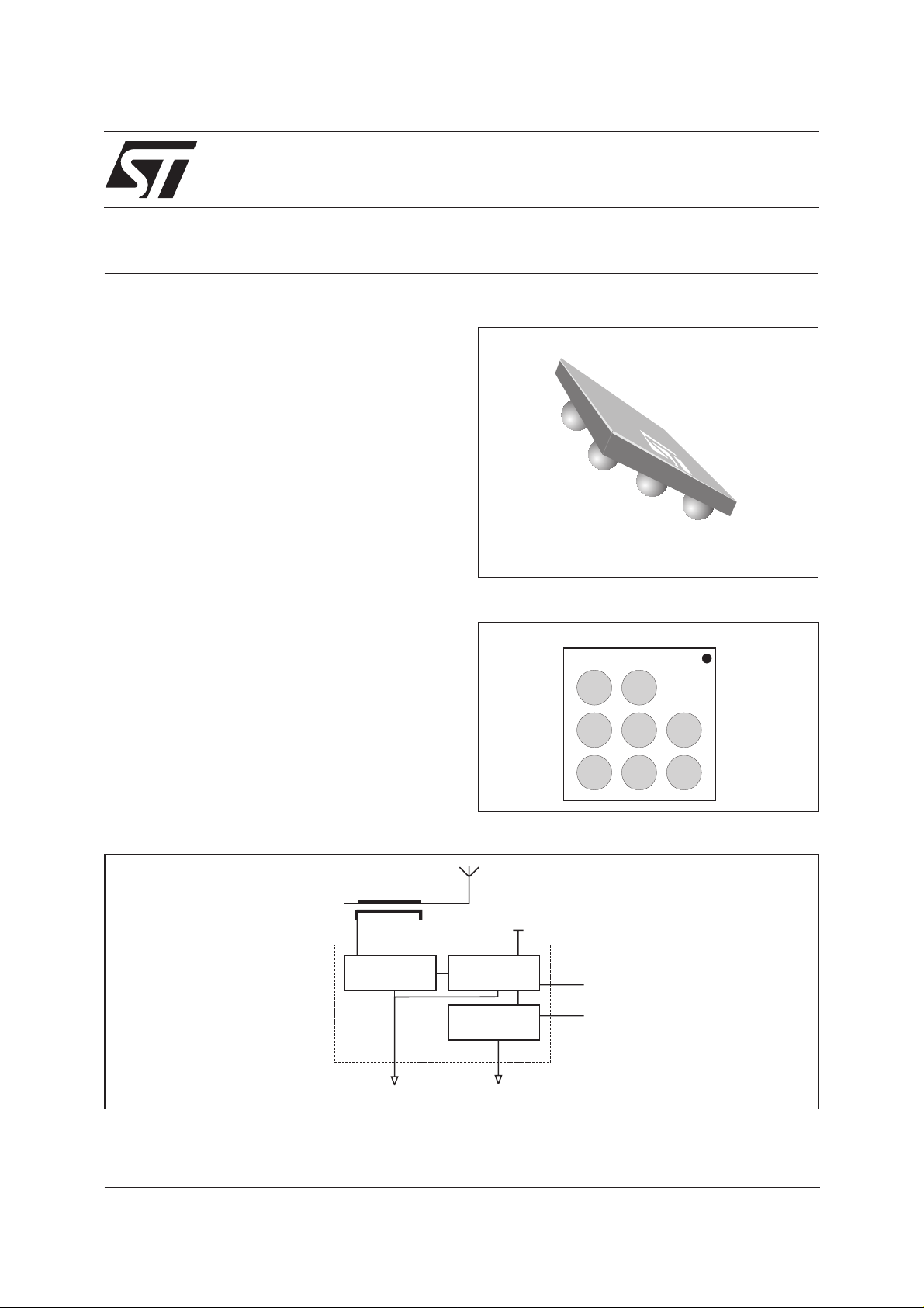
FUNCTIONAL DIAGRAM
Coupler
RF input
RF detector
TM : IPAD is a trademark of STMicroelectronics.
January 2003 - Ed: 1
compensation
STPAC01F1
V
Low pass
filter
Thermal
GND2GND1
BIAS
V
V
DCOut
temp
Gnd1
RFin
Gnd1
Gnd1
Gnd2
Bias
B
C
1/6
Page 2

STPAC01F1
ABSOLUTE RATINGS (Tamb = 25°C)
Symbol Parameter and test conditions Value Unit
V
BIAS
P
RF
F
OP
V
PP
T
OP
T
STG
ELECTRICAL CHARACTERISTICS (Tamb = 25°C)
PARAMETERS RELATED TO BIAS VOLTAGE
Symbol Parameter Test conditions Min. Typ. Max. Unit
V
BIAS
I
BIAS
Bias voltage
RF power at the RF input
Operating frequency range
ESD level as per MIL-STD 883E method 3015.7 notice 8 (HBM)
Operating temperature range
Storage temperature range
Operating bias voltage
Bias current V
BIAS
= 3.2 V
2.2 3.2 V
5V
20 dBm
0.8 to 2 GHz
100 V
-30 to +85 °C
-55 to 150 °C
0.5 mA
PARAMETERS RELATED TO DETECTION FUNCTION (V
= 2.7 V, DC output load = 100 kΩ)
BIAS
Symbol Parameter Test conditions Min. Typ. Max. Unit
V
∆V
DCout
DCout
DC output voltage
(see fig. 1, I
= 50µA)
DC
DCoutput voltage variation
(see fig. 5, I
= 50µA)
DC
F = 1.85 GHz, P
F = 1.85 GHz, P
F = 0.85 GHz, P
F = 0.85 GHz, P
0<T
amb
< 70°C,
F = 1.85 GHz, P
2.2<V
BIAS
< 3.2 V,
F = 1.85 GHz, P
=10dBm
RF
= -20 dBm
RF
=10dBm
RF
= -20 dBm
RF
=10dBm
RF
=10dBm
RF
0.97 1.07 1.17 V
1.83 1.93 2.03
0.78 0.88 0.98
1.83 1.93 2.03
0.09 V
0.44
PARAMETERS RELATED TO TEMPERATURE FUNCTION
Symbol Parameter Test conditions Min. Typ. Max. Unit
V
Temp
Temperature output
IDC= 50µA
1.83 1.93 2.03 V
voltage (see fig. 6)
∆V
Temp
Temperature output
voltage variation
(see fig. 6)
IDC= 50µA,0<T
= 50µA, 2.2 < V
I
DC
amb
BIAS
<70°C
< 3.2 V
0.09 V
0.44
2/6
Page 3

APPLICATION DIAGRAM
Coupler
RF input
STPAC01F1
V
BIAS
IDC= 50µA
RF detector
STPAC01F1
GND1
Low pass
filter
Thermal
compensation
GND2
V
V
DCOut
temp
I
DC
-
+
= 50µA
Out
The STPAC01 is the first part of the power amplifier stage and provides both RF power and die
temperature measurements. The above figure gives the basic circuit of RF detector.
A coupler located on the line between RF amplifier output and the antenna takes a part of the available
power and applies it to STPAC01 RF input.
The RF detector and the low pass filter provide a DC voltage depending on the input power. Thermal
compensation provides a DC voltage dependingon theambient temperature. As the detection system and
the thermal compensation are based on the same topology, VDCout will have the same temperature
variation as Vtemp. Connected to a differential amplifier, the output will be a voltage directly linked to the
RF input power. VDCout and Vtemp must be bias with 50µA DC current.
This topology offers the most accurate output value as it is 100% compensated.
Fig. 1: V
measurement circuit.
DCout
Fig. 2: V
versus RF input power.
DCout
RF generator
Power
supply
Current
generator
RF in
V
BIAS
STPAC
test board
I
DC
V
DCOut
DC output
voltage
Multimeter
VDCout
2
1.8
1.6
1.4
1.2
1
0.8
-20 -15 -10 -5 0 5 10
Tamb = 25°C
Ibias = 50µA
Vbias = 2.7V
850MHz
Pin (dBm)
1850MHz
3/6
Page 4

STPAC01F1
Fig. 3: Relative variation of V
DCout
versus
frequency (from 800 to 900 MHz).
V
(Freq.) / V
DCout
1.05
1
0.95
0.9
800 825 850 875 900
DCOut
(850MHz)
Frequency in MHz
Fig. 5: Temperature effect measurement circuit on
.
V
DCout
Climatic
chamber
V
RF generator
RF in
STPAC
test board
DCOut
Multimeter
Fig. 4: Relative variation of V
DCout
versus
frequency (from 1800 to 1900 MHz).
V
(Freq.) / V
DCout
1.05
1
0.95
0.9
1800 1825 1850 1875 1900
Fig. 6: V
temp
(850MHz)
DCOut
Frequency in MHz
measurement circuit.
Climatic
chamber
STPAC
test board
V
temp
Multimeter
DC output
Power
V
BIAS
voltage
supply
I
Current
DC
generator
Fig. 7: V
output voltage versus ambient
temp
temperature.
Vtemp
1.98
1.96
1.94
1.92
1.9
1.88
0 10203040506070
Tamb (°C)
Ibias = 50µA
Power
supply
Current
generator
V
BIAS
Temp.
voltage
I
DC
4/6
Page 5

PACKAGE MECHANICAL DATA
STPAC01F1
500µm ± 50
1.57mm ± 50µm
FOOT PRINT RECOMMENDATIONS
Copper pad Diameter :
250µm recommended , 300µm max
500µm ± 50
315µm ± 50
1.57mm ± 50µm
MARKING
Dot, ST logo
xxx = marking
yww = datecode
(y = year
ww = week)
650µm ± 65
365
365
240
Solder stencil opening : 330µm
Solder mask opening recommendation :
340µm min for 300µm copper pad diameter
All dimensions in µm
220
xyxwx
w
40
5/6
Page 6

STPAC01F1
FLIP-CHIP TAPE AND REEL SPECIFICATION
Dot identifying Pin A1 location
8 +/- 0.3
yww
xxx
ST
4 +/- 0.1
yww
xxx
ST
Ø 1.5 +/- 0.1
yww
xxx
1.75 +/- 0.1 3.5 +/- 0.1
ST
0.73 +/- 0.05
All dimensions in mm
User direction of unreeling
4 +/- 0.1
OTHER INFORMATION
Ordering code Marking Package Weight Base qty Delivery mode
STPAC01F1 RAT Flip-Chip 3.3 mg 5000 Tape& reel
Note: More packing informations are available in the application note AN1235: ''Flip-Chip: Package description and
recommandations for use''
Informationfurnishedisbelieved to be accurate andreliable.However,STMicroelectronics assumes no responsibility fortheconsequencesof
useofsuchinformation nor for any infringement of patentsorotherrights of third parties which mayresultfromitsuse. No license is granted by
implication or otherwise under any patent or patent rights of STMicroelectronics. Specifications mentioned in this publication are subject to
change without notice. This publication supersedes and replaces all information previously supplied.
STMicroelectronics products are not authorized for use as critical components in life support devices or systems without express written
approval of STMicroelectronics.
The ST logo is a registered trademark of STMicroelectronics
© 2003 STMicroelectronics - Printed in Italy - All rights reserved.
STMicroelectronics GROUP OF COMPANIES
Australia - Brazil - Canada - China - Finland - France - Germany
Hong Kong - India - Israel - Italy - Japan - Malaysia - Malta - Morocco - Singapore
Spain - Sweden - Switzerland - United Kingdom - United States.
http://www.st.com
6/6
 Loading...