

Page 1
STW16NA40
®
STH16NA40FI
N - CHANNEL 400V - 0.21Ω - 16A - TO-247/ISOWATT218
POWER MOS TRANSISTORS
PRELIMINARY DATA
TYPE V
STW16NA40
STH16NA40FI
■
TYPICAL R
■
AVALANCHE RUGG ED TECHNOLO GY
■
100% AVALANCHE TESTED
■
REPETITIVE AVALANCHE DATA AT 100oC
■
APPLICATION ORIENTED
DS(on)
DSS
400 V
400V
= 0.21
CHARACTERIZATION
APPLICATIONS
■
HIGH CURRENT, HIGH SPEED SWITCH ING
■
SWITCH MODE POWER SUPPLY (SMPS)
■
CHOPPER REGULATORS, CONVERTERS,
MOTOR CONTROL, LIGHTING FOR
INDUSTRIAL AND CONSUMER
ENVIRONMENT
R
< 0.3 Ω
< 0.3 Ω
Ω
DS(on)
I
D
16 A
10 A
3
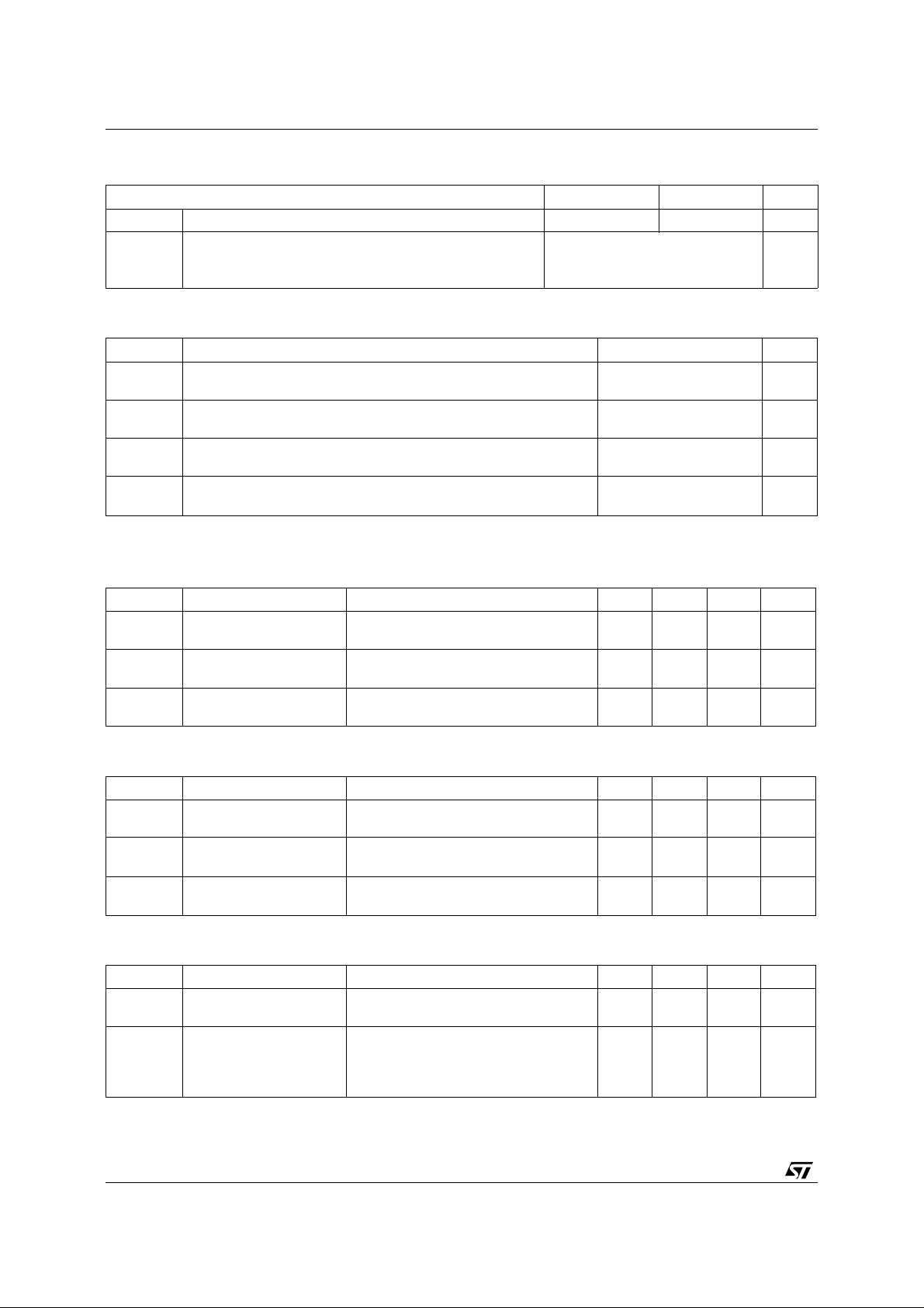
2
1
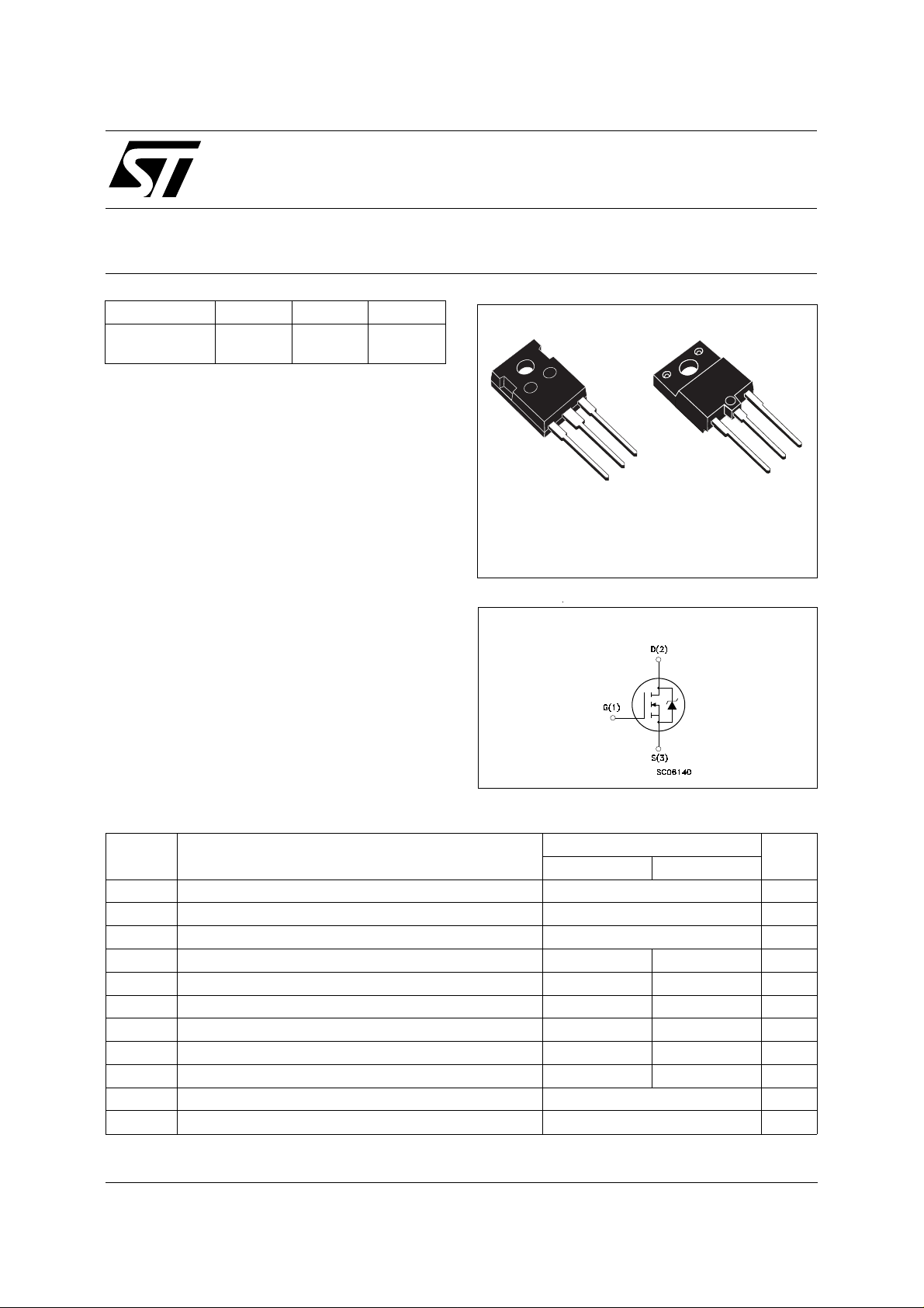
1
TO-247 ISOWATT218
INTERNAL SCHEMATIC DIAGRAM
2
3
ABSOLUTE MAXIMUM RATINGS
Symbol Parameter Value Unit
STW16NA40 STH16NA40FI
400 V
400 V
± 30 V
-65 to 150
150
I
V
V
V
DM
P
Drain-source Voltage (VGS = 0)
DS
Drain- gate Voltage (RGS = 20 kΩ)
DGR
Gate-source Voltage
GS
I
Drain Current (continuous) at Tc = 25 oC
D
I
Drain Current (continuous) at Tc = 100 oC
D
(•)
Drain Current (pulsed)
Total Dissipation at Tc = 25 oC
tot
Derating Factor
V
T
(•) Pulse width limited by safe operating area
Insulation Withstand Voltage (DC)
ISO
Storage Temperature
stg
T
Max. Operating Junction Temperature
j
October 1998
16 10 A
10 7 A
64 64 A
180 70 W
1.44 0.56 W/
4000 V
o
C
o
C
o
C
1/6
Page 2
STW16NA40-STH16NA40FI
THERMAL DATA
TO-247 ISOWATT218
R
thj-case
R
thj-amb
R
thc-sink
T
Thermal Resistance Junction-case Max
Thermal Resistance Junction-ambient Max
Thermal Resistance Case-sink Typ
Maximum Lead Temperature For Soldering Purpose
l
AVALANCHE CHARACTERIST ICS
Symbol Parameter Max Value Unit
I
AR
E
E
I
AR
Avalanche Current, Repetitive or Not-Repetitive
(pulse width limited by T
Single Pulse Avalanche Energy
AS
(starting T
Repetitive Avalanche Energy
AR
= 25 oC, ID = IAR, V
j
(pulse width limited by T
max, δ < 1%)
j
DD
max, δ < 1%)
j
Avalanche Current, Repetitive or Not-Repetitive
= 100 oC, pulse width limited by Tj max, δ < 1%)
(T
c
= 50 V)
0.69 1.78
30
0.1
300
16 A
435 mJ
23 mJ
10 A
o
C/W
o
C/W
o
C/W
o
C
ELECTRICAL CHARACTERISTICS
= 25 oC unless otherwise specified)
(T
case
OFF
Symbol Parameter Test Conditions Min. Typ. Max. Unit
V
(BR)DSS
I
DSS
I
GSS
Drain-source
Breakdown Voltage
Zero Gate Voltage
Drain Current (V
GS
Gate-body Leakage
Current (V
DS
= 0)
= 0)
I
= 250 µA V
D
= Max Rating
V
DS
V
= Max Rating x 0.8 Tc = 100 oC
DS
= ± 30 V
V
GS
GS
= 0
400 V
25
250
±100 nA
ON (∗)
Symbol Parameter Test Conditions Min. Typ. Max. Unit
V
GS(th)
R
DS(on)
I
D(on)
Gate Threshold
Voltage
Static Drain-source On
Resistance
On State Drain Current
= VGS ID = 250 µA
V
DS
VGS = 10V ID = 8 A
V
= 10V ID = 8 A Tc = 100oC
GS
> I
V
DS
V
GS
D(on)
= 10 V
x R
DS(on)max
2.25 3 3.75 V
0.21 0.3
0.6
16 A
DYNAMIC
Symbol Parameter Test Conditions Min. Typ. Max. Unit
g
(∗) Forward
fs
Transconductance
C
C
C
Input Capacitance
iss
Output Capacitance
oss
Reverse Transfer
rss
Capacitance
V
> I
DS
V
DS
x R
D(on)
DS(on)max
= 25 V f = 1 MHz V
ID = 8 A
= 0
GS
912 S
2600
390
120
3500
540
160
µA
µA
Ω
Ω
pF
pF
pF
2/6
®
Page 3

STW16NA40-STH16N A40 FI
ELECTRICAL CHARACTERISTICS
(continued)
SWITCHING ON
Symbol Parameter Test Conditions Min. Typ. Max. Unit
t
d(on)
t
r
(di/dt)
Q
Q
gs
Q
gd
Turn-on Time
Rise Time
on
Turn-on Current Slope
Total Gate Charge
g
Gate-Source Charge
Gate-Drain Charge
V
= 200 V ID = 8 A
DD
= 4.7 Ω VGS = 10 V
R
G
V
= 320 V ID = 16 A
DD
= 47 Ω VGS = 10 V
R
G
V
= 320 V ID = 16 A V
DD
GS
= 10 V
20
18
25
24
380 A/µs
145
15
50
SWITCHING OFF
Symbol Parameter Test Conditions Min. Typ. Max. Unit
t
r(Voff)
t
t
Off-voltage Rise Time
Fall Time
f
Cross-over Time
c
V
= 320 V ID = 16 A
DD
= 4.7 Ω VGS = 10 V
R
G
25
20
45
35
25
60
SOURCE DRAIN DIODE
Symbol Parameter Test Conditions Min. Typ. Max. Unit
16
64
1.6 V
I
SDM
I
SD
Source-drain Current
(•)
Source-drain Current
(pulsed)
V
(∗)
SD
Q
I
RRM
t
Forward On Voltage I
Reverse Recovery
rr
Time
Reverse Recovery
rr
Charge
Reverse Recovery
I
V
SD
SD
DD
Current
(∗) Pulsed: Pulse duration = 300 µs, duty cycle 1.5 %
(•) Pulse width limited by safe operating area
= 16 A VGS = 0
= 16 A di/dt = 100 A/µs
= 100 V Tj = 150 oC
550
9.6
35
ns
ns
nC
nC
nC
ns
ns
ns
A
A
ns
µC
A
®
3/6
Page 4

STW16NA40-STH16NA40FI
TO-247 MECHANICAL DATA
DIM.
MIN. TYP. MAX. MIN. TYP. MAX.
A 4.7 5.3 0.185 0.209
D 2.2 2.6 0.087 0.102
E 0.4 0.8 0.016 0.031
F 1 1.4 0.039 0.055
F3 2 2.4 0.079 0.094
F4 3 3.4 0.118 0.134
G 10.9 0.429
H 15.3 15.9 0.602 0.626
L 19.7 20.3 0.776 0.779
L3 14.2 14.8 0.559 0.413 0.582
L4 34.6 1.362
L5 5.5 0.217
M 2 3 0.079 0.118
Dia 3.55 3.65 0.140 0.144
mm inch
4/6
P025P
®
Page 5

STW16NA40-STH16NA40FI
ISOWATT218 MECHANICAL DATA
DIM.
MIN. TYP. MAX. MIN. TYP. MAX.
A 5.35 5.65 0.210 0.222
C 3.3 3.8 0.130 0.149
D 2.9 3.1 0.114 0.122
D1 1.88 2.08 0.074 0.081
E 0.75 1 0.029 0.039
F 1.05 1.25 0.041 0.049
G 10.8 11.2 0.425 0.441
H 15.8 16.2 0.622 0.637
L1 20.8 21.2 0.818 0.834
L2 19.1 19.9 0.752 0.783
L3 22.8 23.6 0.897 0.929
L4 40.5 42.5 1.594 1.673
L5 4.85 5.25 0.190 0.206
L6 20.25 20.75 0.797 0.817
M 3.5 3.7 0.137 0.145
N 2.1 2.3 0.082 0.090
U4.6 0.181
mm inch
L3
N
E
A
D
C
L5
L2
L6
D1
F
M
U
H
G
123
L1
L4
P025C
®
5/6
Page 6

STW16NA4 0-ST H16 NA4 0FI
Information furnished is believed to be accurate and reliable. However, STMicroelectronics assumes no responsibility for the consequences
of use of such inform ation nor for any in fringe ment o f patents or other rig hts of third par ties wh ich may result from its u se. N o li cen se is
granted by implication or otherwise under any patent or patent rights of STMicroelectronics. Specification mentioned in this publication are
subject to change without notice. This publication supersedes and replaces all information previously supplied. STMicroelectronics products
are not authorized f or use as critical components in life support devices or systems without express written approval of STMicroelectronics.
The ST logo is a registered trademark of STMicroelectronics
© 1998 STMicroelectro nics – Printed in Italy – All Rights Reserved
STMicroelectronics GROUP OF COMPANIES
Australia - Brazil - Canada - China - France - Germany - Italy - Japan - Korea - Malaysia - Malta - Mexico - Morocco - The Netherlands -
Singapore - Spain - Sweden - Switzerland - Taiwan - Thailand - United Kingdom - U.S.A.
http://www.st.com
.
6/6
®
 Loading...