

Page 1
查询STGD3NB60M供应商
STGP3NB60M - STGD3NB60M
N-CHANNEL 3A - 600V TO-220 / DPAK
PowerMESH™ IGBT
TYPE
STGP3NB60M
STGD3NB60M
■ HIGH INPUT IMPEDANCE
■ LOW ON-VOLTAGE DROP (V
■ OFF LOSSES INCLUDE TAIL CURRENT
■ LOW GATE CHARGE
■ HIGH CURRENT CAPABILITY
■ HIGH FREQUENCY OPERATION
■ CO-PACKAGED WITH TURBOSWITCH™
V
CES
600 V
600 V
V
CE(sat) (Max)
@25°C
< 1.9 V
< 1.9 V
cesat
)
I
C
@100°C
3A
3A
ANTIPARALLEL DIODE
DESCRIPTION
Using the latest high voltage technology based on a
patented strip layout, STMicroelectronics has designed an advanc ed family of IGBTs, the PowerMESH™ IGBTs, with outstanding perfomances.
The suffix "M" identifies a family optimized to
achieve very low switc hing switching times for high
frequency applications (<20KHZ)
3
1
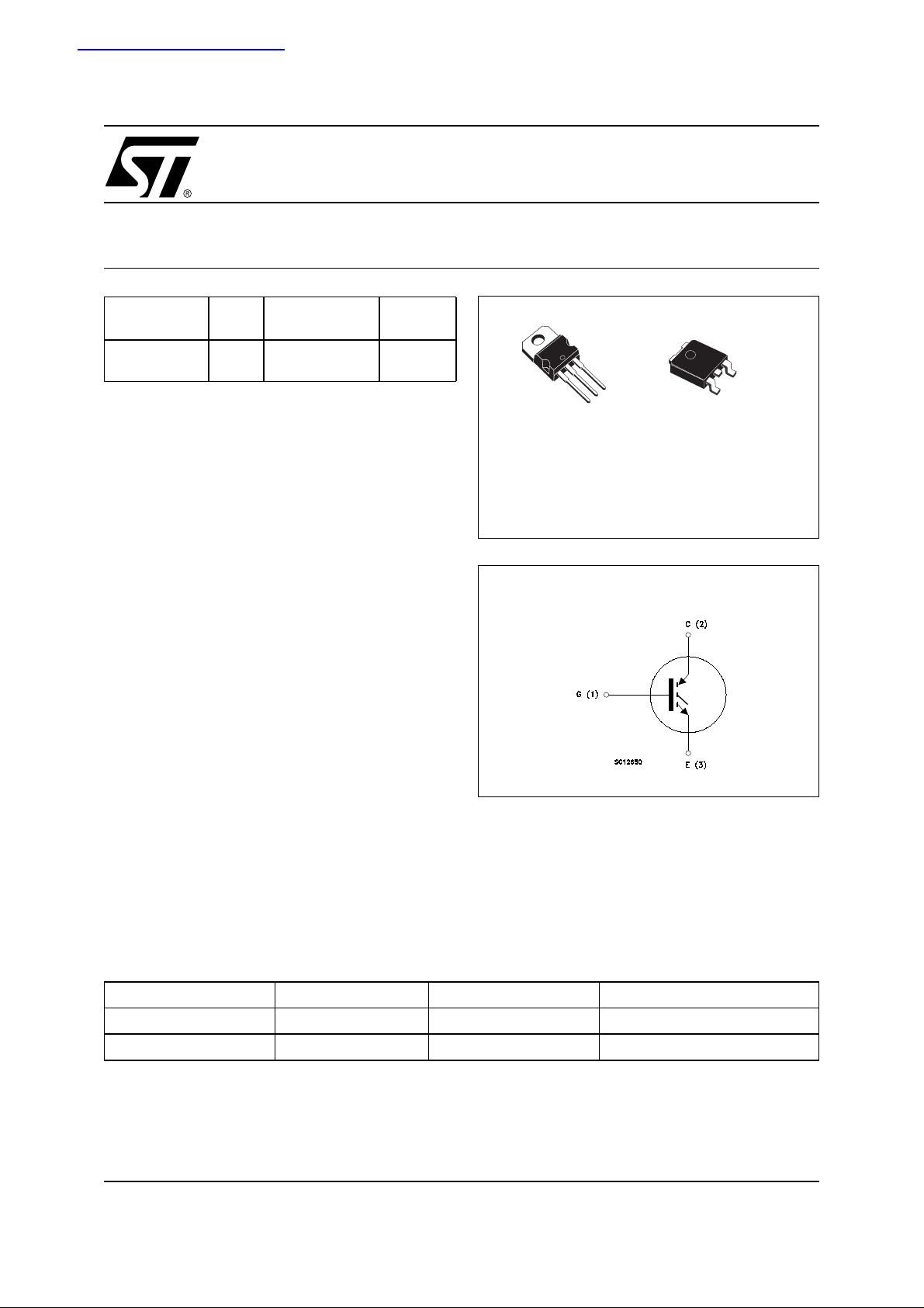
TO-220
3
2
1
DPAK
INTERNAL SCHEMATIC DIAGRAM
APPLICATIONS
■ MOTOR CONTROLS
■ SMPS AND PFC AND BOTH HARD SWITCH
AND RESONANT TOPOLOGIES
ORDERING INFORMATION
SALES TYPE MARKING PACKAGE PACKAGING
STGP3NB60M GP3NB60M TO-220 TUBE
STGD3NB60MT4 GD3NB60M DPAK TAPE & REEL
1/11June 2003
Page 2
STGP3NB60M - STG D3NB60M
ABSOLUTE MAXIMUM RATINGS
Symbol Parameter Value Unit
TO-220 DPAK
V
CES
V
I
I
I
CM
P
TOT
T
T
() Pulse width limited by safe operating area
THERMAL DATA
Rthj-case Thermal Resistance Junction-case Max 1.8 2.1 °C/W
Rthj-amb Thermal Resistance Junction-ambient Max 62.5 100 °C/W
Collector-Emitter Voltage (VGS=0)
Gate-Emitter Voltage ±20 V
GE
Collector Current (continuous) at TC=25°C
C
Collector Current (continuous) at TC=100°C
C
()
Collector Current (pulsed) 24 A
Total Dissipation at TC= 25°C
68 60 W
600 V
6A
3A
Derating Factor 0.55 0.47 W/°C
Storage Temperature – 55 to 150 °C
stg
Max. Operating Junction Temperature 150 °C
j
TO-220 DPAK
ELECTRICAL CHARACTERISTICS (T
= 25 °C UNLESS OTHERWISE SPECIFIED)
CASE
OFF
Symbol Parameter Test Conditions Min. Typ. Max. Unit
V
BR(CES)
Collector-Emitter Breakdown
IC= 250 µA, VGE=0 600 V
Voltage
I
CES
I
GES
Collector cut-off
=0)
(V
GE
Gate-Emitter Leakage
Current (V
CE
=0)
V
= Max Rating, TC=25°C
CE
VCE= Max Rating, TC= 125 °C
V
=±20V,VCE= 0 ±100 nA
GE
50 µA
100 µA
ON (1)
Symbol Parameter Test Conditions Min. Typ. Max. Unit
V
GE(th)
V
CE(sat)
Gate Threshold Voltage
Collector-Emitter Saturation
Voltage
V
CE=VGE,IC
VGE= 15V, IC=3A
VGE= 15V, IC= 3 A, Tj =125°C
=250µA
35V
1.5 1.9 V
1.2 V
2/11
Page 3
STGP3NB60M - STG D3NB60M
ELECTRICAL CHARACTERISTICS (CONTINUED)
DYNAMIC
Symbol Parameter Test Conditions Min. Typ. Max. Unit
(1)
g
fs
C
ies
C
oes
C
res
Forward Transconductance
Input Capacitance
Output Capacitance 33 pF
Reverse Transfer
Capacitance
Q
Q
ge
Q
gc
I
CL
Total Gate Charge
g
Gate-Emitter Charge
Gate-Collector Charge
Latching Current V
SWITCHING ON
Symbol Parameter Test Conditions Min. Typ. Max. Unit
t
d(on)
t
(di/dt)
Eon
r
Turn-on Delay Time
Rise Time
Turn-on Current Slope
on
Turn-on Switching Losses
VCE=15V,Ic=3A
V
=25V,f=1MHz,VGE=0
CE
= 480V, IC=3A,
V
CE
=15V
V
GE
= 480 V, VGE=15V
clamp
Tj = 125°C , RG=10Ω
= 480 V, IC= 3A, RG=10Ω
V
CC
,VGE=15V
=480V,IC=3ARG=10Ω
V
CC
V
= 15 V,Tj =125°C
GE
5S
240 pF
6pF
15
20
2.2
8
20 A
10
4
570
30
nC
nC
nC
ns
ns
A/µs
µJ
SWITCHING OFF
Symbol Parameter Test Conditions Min. Typ. Max. Unit
V
t
c
t
r(Voff
t
d(off
t
f
(**)
E
off
E
ts
t
c
t
r(Voff
td(
off
t
f
E
(**)
off
E
ts
Note: 1. Pulsed: Pulse duration = 300 µs, duty cycle 1.5 %.
2. Pulse width limited by max. junction temperature.
(**)Losses include Also the Tail (Jedec Standardization)
Cross-over Time
)
Off Voltage Rise Time 85 ns
)
Delay Time 120 ns
Fall Time 240 ns
Turn-off Switching Loss 175
Total Switching Loss 205
Cross-over Time
)
Off Voltage Rise Time 270 ns
)
Delay Time 344 ns
Fall Time 515 ns
Turn-off Switching Loss 458
Total Switching Loss 488
=480V,IC=3A,
cc
R
=10Ω,VGE=15V
G
V
=480V,IC=3A,
cc
R
=10Ω,VGE=15V
G
Tj = 125 °C
330 ns
810 ns
µJ
µJ
µJ
µJ
3/11
Page 4
STGP3NB60M - STG D3NB60M
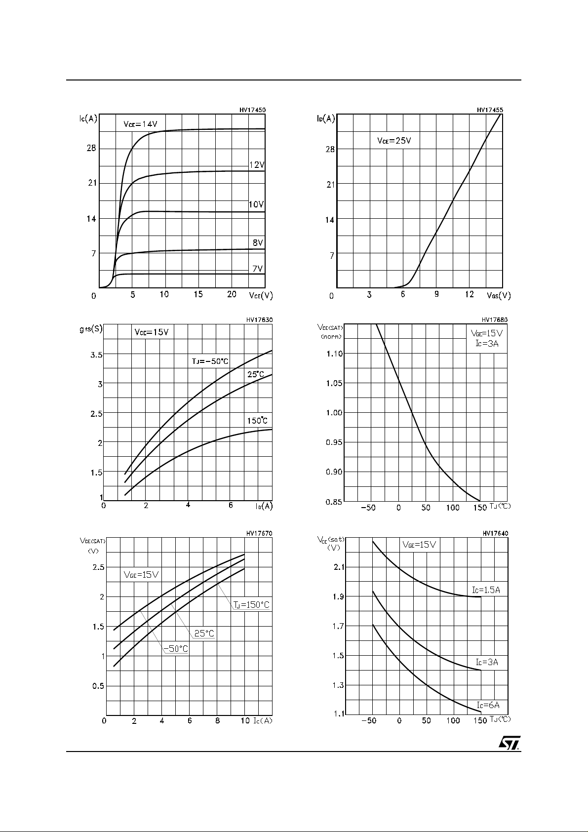
Output Characteristics
Transfer Characteri stics
Normalized Co llecto r-Emitter On Voltage vs Temp .Transconductance
Collector-Emitter On Voltage vs Collector Current
4/11
Collector-Emitter On V oltage vs Temperature
Page 5

STGP3NB60M - STG D3NB60M
Gate Threshold vs Temperatur e
Normalized Breakdown Voltage vs Temperature
Gate Charge vs Gate-Emitter VoltageCapacitance Variations
Total Switching Losses vs Gate Resistance
Total Switching Losses vs Temperature
5/11
Page 6

STGP3NB60M - STG D3NB60M
Total Switching Losses vs Collector Current
Thermal Impedance for TO-220
Turn-Off SOAThermal Impedance for DPAK
6/11
Page 7

STGP3NB60M - STG D3NB60M
Fig. 2: Test Circuit For Induc t ive Load SwitchingFig. 1: Gate Charge test Circuit
7/11
Page 8

STGP3NB60M - STG D3NB60M
TO-220 MECHANICAL DATA
DIM.
A 4.40 4.60 0.173 0.181
b 0.61 0.88 0.024 0.034
b1 1.15 1.70 0.045 0.066
c 0.49 0.70 0.019 0.027
D 15.25 15.75 0.60 0.620
E 10 10.40 0.393 0.409
e 2.40 2.70 0.094 0.106
e1 4.95 5.15 0.194 0.202
F 1.23 1.32 0.048 0.052
H1 6.20 6.60 0.244 0.256
J1 2.40 2.72 0.094 0.107
L 13 14 0.511 0.551
L1 3.50 3.93 0.137 0.154
L20 16.40 0.645
L30 28.90 1.137
øP 3.75 3.85 0.147 0.151
Q 2.65 2.95 0.104 0.116
MIN. TYP MAX. MIN. TYP. MAX.
mm. inch
8/11
Page 9

STGP3NB60M - STG D3NB60M
P032P_B
TO-252 (DPAK) MECHANICAL DATA
DIM.
A 2.20 2.40 0.087 0.094
A1 0.90 1.10 0.035 0.043
A2 0.03 0.23 0.001 0.009
B 0.64 0.90 0.025 0.035
B2 5.20 5.40 0.204 0.213
C 0.45 0.60 0.018 0.024
C2 0.48 0.60 0.019 0.024
D 6.00 6.20 0.236 0.244
E 6.40 6.60 0.252 0.260
G 4.40 4.60 0.173 0.181
H 9.35 10.10 0.368 0.398
L2 0.8 0.031
L4 0.60 1.00 0.024 0.039
V2 0
MIN. TYP. MAX. MIN. TYP. MAX.
o
mm inch
o
8
o
0
o
0
9/11
Page 10

STGP3NB60M - STG D3NB60M
DPAK FOOTPRINT
All dimensions are in m illimeters
TAPE AND REEL SHIPMENT (suffix ”T4”)*
TUBE SHIPMENT (no suffix)*
All dimensions
are in millimeters
REEL MECHANICAL DATA
DIM.
A 330 12.992
B 1.5 0.059
C 12.8 13.2 0.504 0.520
D 20.2 0.795
G 16.4 18.4 0.645 0.724
N 50 1.968
T 22.4 0.881
mm inch
MIN. MAX. MIN. MAX.
TAPE MECHANICAL DATA
DIM.
A0 6. 8 7 0.267 0.275
B0 10.4 10.6 0.409 0.417
B1 12.1 0.476
D 1.5 1.6 0.059 0.063
D1 1.5 0.059
E 1.65 1.85 0.065 0.073
F 7. 4 7.6 0.291 0.299
K0 2.55 2.75 0.100 0.108
P0 3. 9 4.1 0.153 0.161
P1 7.9 8.1 0.311 0.319
P2 1. 9 2.1 0.075 0.082
R 40 1.574
W 15.7 16.3 0.618 0.641
* on sales ty pe
10/11
mm inch
MIN. MAX. MIN. MAX.
BASE QTY BULK QTY
2500 2500
Page 11

STGP3NB60M - STG D3NB60M
Information furnished is believed to be accurate and reliable. However, STMicroelectronics assumes no responsibility for the
consequences of u se of such inf ormat ion nor for any in fring ement of p aten ts or othe r ri ghts of th ird p arties whic h may resul t f rom
its use. No license is granted by implication or otherwise under any patent or patent rights of STMicroelectronics. Specifications
mentioned in this publication are subject to change without notice. This publication supersedes and replaces all information
previously supplied. STMicroelectronics products are not authorized for use as critical components in life support devices or
systems without express written approval of STMicroelectronics.
Australia - Brazil - Canada - China - Finland - France - Germany - Hong Kong - India - Israel - Italy - Japan - Malaysia - Malta - Morocco
© The ST logo is a registered trademark of STMicroelectronics
© 2003 STMicroelectronics - Printed in Italy - All Rights Reserved
Singapore - Spain - Sweden - Switzerland - United Kingdom - United States.
STMicroelectronics GROUP OF COMPANIES
© http://www.st.com
11/11
 Loading...