

Page 1
STGP20NB60K
N-CHANNEL 20A - 600V - TO-220
PowerMesh IGBT
PRELIMINARY DATA
TYPE V
CES
V
CE(sat)
I
C
STGP20NB60K 600 V < 2.8 V20A
■ HIGH INPUT IMPEDANCE (VOLTAGE DRIVEN)
■ LOW ON-VOLTAGE DROP (V
■ LOW ON-LOSSES
■ LOW GATECHARGE
■ HIGH CURRENT CAPABILITY
■ OFF LOSSES INCLUDE TAIL CURRENT
■ VERY HIGH FREQUENCY OPERATION
■ SHORT CIRCUIT RATED
■ LATCH CURRENT FREE OPERATION
cesat
)
DESCRIPTION
Using thelatest highvoltage technology basedon a
patented strip layout, STMicroelectronics has
designed an advanced family of IGBTs, the
PowerMESHIGBTs, with outstanding
performances. The suffix “K” identifies a family
optimized for high frequency motor control
applications with short circuit withstand capability.
APPLICATIONS
■ HIGH FREQUENCY MOTOR CONTROLS
■ U.P.S.
■ WELDING EQUIPMENTS
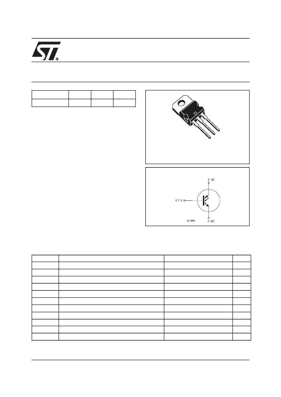
3
2
1
TO-220
INTERNAL SCHEMATIC DIAGRAM
ABSOLUTE MAXIMUM RATINGS
Symbol Parameter Value Unit
V
CES
V
ECR
V
GE
I
C
I
C
I
CM
Tsc Short Circuit Withstand 10
P
TOT
T
stg
T
j
June 2000
This is preliminary information on a new product now in development or undergoing evaluation. Details are subject to change without notice.
Collector-Emitter Voltage (VGS=0)
600 V
Emitter-Collector Voltage 20 V
Gate-Emitter Voltage ±20 V
Collector Current (continuos) at TC=25°C
Collector Current (continuos) at TC= 100°C
(■)
Collector Current (pulsed) 80 A
TotalDissipation at TC=25°C
40 A
20 A
125 W
Derating Factor 1 W/°C
Storage Temperature –65 to 150 °C
Max. Operating Junction Temperature 150 °C
µs
1/6
Page 2
STGP20NB60K
THERMAL DATA
Rthj-case Thermal Resistance Junction-case Max 1.0 °C/W
Rthj-amb Thermal Resistance Junction-ambient Max 62.5 °C/W
Rthc-h Thermal Resistance Case-heatsink Typ 0.5 °C/W
ELECTRICAL CHARACTERISTICS (TCASE = 25 °C UNLESS OTHERWISE SPECIFIED)
OFF
Symbol Parameter Test Conditions Min. Typ. Max. Unit
V
BR(CES)
I
CES
I
GES
ON (1)
Symbol Parameter Test Conditions Min. Typ. Max. Unit
V
GE(th)
V
CE(sat)
Collectro-Emitter Breakdown
Voltage
Collector cut-off
(V
=0)
GE
Gate-Emitter Leakage
Current (V
CE
=0)
Gate Threshold Voltage
Collector-Emitter Saturation
Voltage
I
= 250 µA, VGE=0
C
= Max Rating, TC=25°C
V
CE
V
= Max Rating, TC= 125 °C
CE
= ±20V , VCE=0
V
GE
V
CE=VGE,IC
V
= 15V, IC=20A
GE
V
=15V, IC= 20 A, Tj =125°C
GE
= 250µA
600 V
10 µA
100 µA
±100 nA
57V
2.3 2.8 V
1.9 V
DYNAMIC
Symbol Parameter Test Conditions Min. Typ. Max. Unit
g
fs
C
ies
C
oes
C
res
Q
g
Q
ge
Q
gc
twsc
Forward Transconductance
Input Capacitance
Output Capacitance 200 pF
Reverse Transfer
Capacitance
TotalGate Charge
Gate-Emitter Charge T.B.D. nC
Gate-Collector Charge T.B.D. nC
Short Circuit Withstand Time
V
=25V,IC=20 A
CE
= 25V, f = 1 MHz, VGE=0
V
CE
V
= 480V, IC=20A,
CE
= 15V
V
GE
V
= 0.5 BVces , VGE=15V,
ce
Tj = 125°C,R
=10Ω
G
8S
1300 pF
30 pF
90 nC
10 µs
SWITCHING ON
Symbol Parameter Test Conditions Min. Typ. Max. Unit
t
d(on)
t
r
(di/dt)
Eon Turn-on Switching Losses 300 µJ
Turn-on Delay Time
Rise Time 70 ns
Turn-on Current Slope
on
V
= 480 V, IC=20A
CC
=10Ω,VGE=15V
R
G
V
= 480V, IC=20ARG=10Ω
CC
= 15 V,Tj= 125°C
V
GE
20 ns
350 A/µs
2/6
Page 3

STGP20NB60K
ELECTRICAL CHARACTERISTICS (CONTINUED)
SWITCHING OFF
Symbol Parameter Test Conditions Min. Typ. Max. Unit
t
c
t
r(Voff
t
d(off
t
f
E
(**)
off
E
ts
t
c
t
r(Voff
t
d(off
t
f
E
(**)
off
E
ts
Note: 1. Pulsed: Pulse duration = 300 µs, duty cycle 1.5%.
2. Pulse width limited by max. junction temperature.
(**)Losses include Also the Tail (Jedec Standardization)
Cross-over Time
120 ns
) Off Voltage Rise Time 35 ns
= 480 V, IC=20A,
V
) Delay Time 130 ns
cc
=10Ω,VGE=15V
R
GE
Fall Time 80 ns
Turn-off Switching Loss 0.45 mJ
TotalSwitching Loss 0.6 mJ
Cross-over Time
V
)
Off Voltage Rise Time 55 ns
)
Delay Time 160 ns
= 480 V, IC=20A,
cc
=10Ω,VGE=15V
R
GE
Tj = 125 °C
190 ns
Fall Time 150 ns
Turn-off Switching Loss 0.75 mJ
TotalSwitching Loss 1.05 mJ
3/6
Page 4

STGP20NB60K
Fig. 2: Test Circuit For Inductive Load SwitchingFig. 1: Gate Charge test Circuit
4/6
Page 5

TO-220 MECHANICAL DATA
STGP20NB60K
DIM.
A 4.40 4.60 0.173 0.181
C 1.23 1.32 0.048 0.051
D 2.40 2.72 0.094 0.107
D1 1.27 0.050
E 0.49 0.70 0.019 0.027
F 0.61 0.88 0.024 0.034
F1 1.14 1.70 0.044 0.067
F2 1.14 1.70 0.044 0.067
G 4.95 5.15 0.194 0.203
G1 2.4 2.7 0.094 0.106
H2 10.0 10.40 0.393 0.409
L2 16.4 0.645
L4 13.0 14.0 0.511 0.551
L5 2.65 2.95 0.104 0.116
L6 15.25 15.75 0.600 0.620
L7 6.2 6.6 0.244 0.260
L9 3.5 3.93 0.137 0.154
DIA. 3.75 3.85 0.147 0.151
MIN. TYP. MAX. MIN. TYP. MAX.
A
C
mm inch
E
D
L5
L7
Dia.
D1
L6
L2
L9
L4
F2
F1
G1
H2
G
F
P011C
5/6
Page 6

STGP20NB60K
6/6
Information furnished isbelieved to be accurate andreliable. However, STMicroelectronics assumes no responsibility for the consequences
of use of such information nor for any infringement of patents or other rights of third parties which may result from its use. No license is
granted by implication or otherwise underany patent or patent rights of STMicroelectronics. Specification mentioned inthis publication are
subject to change without notice. This publication supersedes and replaces all information previously supplied. STMicroelectronics products
are not authorized for use ascritical components in life support devices or systems withoutexpress written approval of STMicroelectronics.
Australia -Brazil - China - Finland- France- Germany - Hong Kong - India- Italy - Japan - Malaysia - Malta -Morocco -
The ST logo is a trademark of STMicroelectronics
2000 STMicroelectronics – Printed in Italy – All Rights Reserved
STMicroelectronicsGROUP OF COMPANIES
Singapore - Spain - Sweden - Switzerland - United Kingdom - U.S.A.
http://www.st.com
 Loading...