

Page 1
STGP10NB37LZ
N-CHANNEL CLAMPED 20A - TO-220
INTERNALLY CLAMPED PowerMesh™ IGBT
TYPE V
CES
V
CE(sat)
I
C
STGP10NB37LZ CLAMPED < 1.8 V 20 A
■ POLYSILIC ON GA TE VOLT AG E DRI VEN
■ LOW THRESHOLD VOLTA GE
■ LOW ON-VOLTAGE DROP
■ LOW GATE CHARGE
■ HIGH CURRENT CAPABILITY
■ HIGH VOLTAGE CLAMPING FEATURE
DESCRIPTION
Using the latest high voltage technology based on a
patented strip layout, STMicroelectronics has
designed an advanced family of IGBTs, the
PowerMESH
™
IGBTs, with outstanding
performances. The built in collector-gate zener
exhibits a very precise active clamping while the
gate-emitter zener supplies an ESD protection.
APPLICATIONS
■ AUTOMO TIVE IGNI TI ON
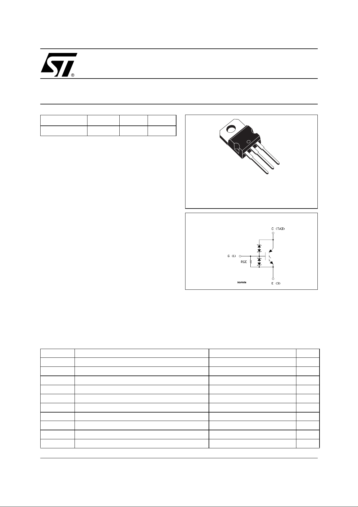
3
2
1
TO-220
INTERNAL SCHEMATIC DIAGRAM
ABSOLUTE MAXIMUM RATINGS
Symbol Parameter Value Unit
V
V
P
V
I
E
T
CES
ECR
GE
I
C
CM
TOT
SD
stg
T
j
Collector-Em itter Voltage (VGS = 0)
CLAMPED V
Reverse Battery Protection 18 V
Gate-Emitter Voltage CLAMPED V
Collector Current (continuos) at TC = 100°C
20 A
Collector Current (pulse width < 100µs) 60 A
Total Dissipation at TC = 25°C
125 W
Derating Factor 0.83 W/°C
ESD (Human Body Model) 4 KV
Storage Temperature –65 to 175 °C
Max. Operating Junction Temperature 175 °C
1/9November 2000
Page 2
STGP10NB37LZ
THERMA L D ATA
Rthj-case Thermal Resistance Junction-case Max 1.2 °C/W
Rthj-amb Thermal Resistance Junction-ambient Max 62.5 °C/W
Rthc-sink Thermal Resistance Case-sink Typ 0.2 °C/W
ELECTRICAL CHARACTERISTICS (TCASE = 25 °C UNLESS OTHERWISE SPECIFIED)
OFF
Symbol Parameter Test Conditions Min. Typ. Max. Unit
BV
(CES)
Clamped Voltage IC = 2 mA, VGE = 0,
Tj= - 40°C to 150°C
= 75 mA, VGE = 0,
I
EC
Tj= - 40°C to 150°C
= ± 2 mA
I
G
Tj= - 40°C to 150°C
V
= 15 V, VGE =0 ,Tj =150 °C
CE
VCE =200 V, VGE=0 ,TC =150°C
V
= ± 10V , VCE = 0 ± 700 µA
GE
ON
BV
BV
I
I
R
(1)
(ECR)
GE
CES
GES
GE
Emitter Collector Break-down
Voltage
Gate Emitter Break-down
Voltage
Collector cut-off Current
= 0)
(V
GE
Gate-Emitter Leakage
Current (V
CE
= 0)
Gate Emitter Resistance 20 K
Symbol Parameter Test Conditions Min. Typ. Max. Unit
V
GE(th)
Gate Threshold Voltage VCE = VGE, IC = 250µA,
Tj= - 40°C to 150°C
V
CE(SAT)
I
Collector-Emitter Saturation
Voltage
C
Collector Current
VGE =4.5V, IC = 10 A, Tj= 25°C
VGE =4.5V, IC = 10 A, Tc= -40°C
V
= 4.5V, VCE = 9 V
GE
375 400 425 V
18 V
12 16 V
10 µA
100 µA
0.6 2.4 V
1.2 1.8 V
1.3 V
20 A
Ω
DYNAMIC
Symbol Parameter Test Conditions Min. Typ. Max. Unit
V
= 15 V , IC=20 A
CE
V
= 25V, f = 1 MHz, VGE = 0
CE
VGE = 5V
18 S
1250 pF
18 pF
28 nC
2/9
g
fs
C
ies
C
oes
C
res
Q
g
Forward Transconductance
Input Capacitance
Output Capacitance 103 pF
Reverse Transfer
Capacitance
Gate Charge VCE = 320V, IC = 10 A,
Page 3
STGP10NB37LZ
FUNCTIONAL CHARACTERISTICS
Symbol Parameter Test Conditions Min. Typ. Max. Unit
I
L
Latching Current V
U.I.S. Unclamped Inductive
Switching Current
SWITCHING ON
Symbol Parameter Test Conditions Min. Typ. Max. Unit
t
d(on)
t
(di/dt)
Eon
r
Turn-on Delay Time
Rise Time 340 ns
Turn-on Current Slope
on
Turn-on Switching Losses
SWITCHING OFF
Symbol Parameter Test Conditions Min. Typ. Max. Unit
t
c
t
(V
r
off
td(
off
t
f
E
(**)
off
t
c
tr(V
off
td(
off
t
f
E
(**)
off
(●)Pulsed: P ul se duration = 300 µ s, duty cycle 1.5 %. (1)Pulse width lim i t ed by max. ju nction temperature. (* *)Losses Include Also the Tail
Cross-over Time
)
Off Voltage Rise Time 2.2 µ s
)
Delay Time 14.8 µs
Fall Time 1.5 µs
Turn-off Switching Loss 4.0 mJ
Cross-over Time
)
Off Voltage Rise Time 2.8 µ s
)
Delay Time 15.8 µs
Fall Time 2µs
Turn-off Switching Loss 6.5 mJ
= 320 V, TC = 125 °C
Clamp
R
=1KΩ , VGE = 5 V
GOFF
L = 300µH
=1KΩ , L = 1.6 mH ,
R
GOFF
Tc= 125°C, Vcc = 30V
V
= 320 V, IC = 10 A
CC
RG=1KΩ , VGE = 5 V
= 320 V, IC = 10 A
V
CC
R
=1KΩ, VGE = 5 V
G
V
= 320 V, IC = 10 A,
clamp
R
= 1K Ω , VGE = 5 V
GE
V
= 320 V, IC = 10 A,
clamp
RGE = 1KΩ , VGE = 5 V
Tj = 125 °C
20 A
15 A
520 ns
17
A/µs
180
4µs
5.2 µs
µJ
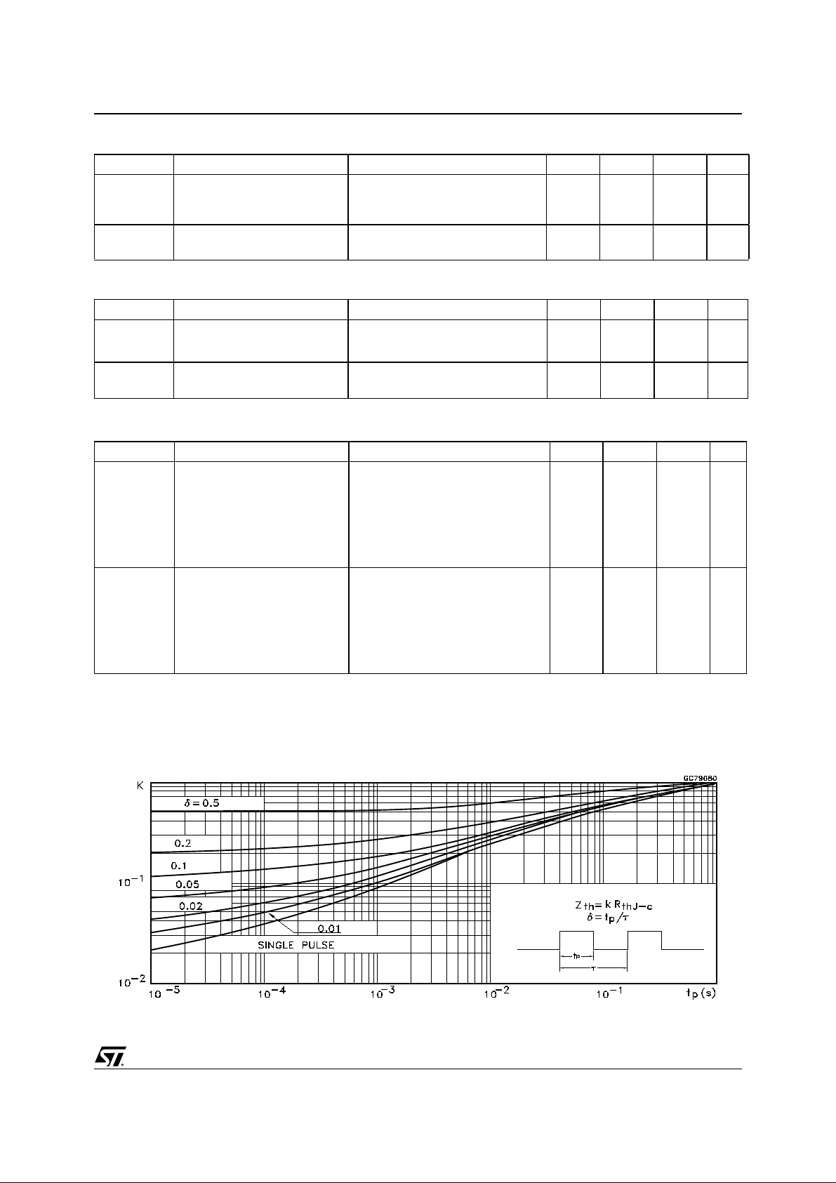
Normalized Transient Thermal Impe dan ce
3/9
Page 4

STGP10NB37LZ
Output Characteristics
Normaliz e d Gat e Threshold V oltage vs Temp. Transc ond uctance
Transfer Characteristics
Normalized Collector-Emitter On Voltage vs
Temperature
4/9
Normalized Collector-Emitter On Voltage vs
Gate-E mit t er Vo l t age
Page 5

STGP10NB37LZ
Capacitance Variations
Off Losses vs Gate Resistance
Gate Charge vs Gate-Emitter Voltage
Off Losses vs Collector Current
Normalized Break-down Voltage vs Temp .
Clamping Voltage vs Gate Resistance
5/9
Page 6

STGP10NB37LZ
Self Clamped Inductive Switching IMAX vs
Open Secondary Coil
6/9
Page 7

And Diode Recovery Times
STGP10NB37LZ
Fig. 2: Unclamped Inductive WaveformFig. 1: Unclamped Inductive Load Test Circuit
Fig. 4: Gate Charge test CircuitFig. 3: Test Circuit For Inductive Load Switching
7/9
Page 8

STGP10NB37LZ
E
TO-220 MECHANICAL DATA
DIM.
A 4.40 4.60 0.173 0.181
C 1.23 1.32 0.048 0.051
D 2.40 2.72 0.094 0.107
D1 1.27 0.050
E 0.49 0.70 0.019 0.027
F 0.61 0.88 0.024 0.034
F1 1.14 1.70 0.044 0.067
F2 1.14 1.70 0.044 0.067
G 4.95 5.15 0.194 0.203
G1 2.4 2.7 0.094 0.106
H2 10.0 10.40 0.393 0.409
L2 16.4 0.645
L4 13.0 14.0 0.511 0.551
L5 2.65 2.95 0.104 0.116
L6 15.25 15.75 0.600 0.620
L7 6.2 6.6 0.244 0.260
L9 3.5 3.93 0.137 0.154
DIA. 3.75 3.85 0.147 0.151
MIN. TYP. MAX. MIN. TYP. MAX.
mm inch
A
C
D
8/9
L5
Dia.
L7
D1
L6
L2
L9
F1
G1
F
H2
G
F2
L4
P011C
Page 9

STGP10NB37LZ
Information furnished is believed to be accurate and reliable. However, STMicroelectronics assumes no responsibility for the consequences
of use of such informa tion n or for an y infring ement of patent s or other rig hts of third part ies which may resu lt from its use . No l i cen se i s
granted by implication or otherwise under any patent or patent rights of STMicroelectronics. Specification mentioned in this publication are
subject to change without notice. This publication supersedes and replaces all information previously supplied. STMicroelectronics products
are not authorized for use as critical compo nents in life support devices or systems without express written approval of STMicroelectronics.
Australia - Brazil - China - Finland - France - Germany - Hong Kong - India - Italy - Japan - Malaysia - Malta - Morocco -
The ST logo is a trademark of STMicroelectronics
© 2000 STMicroelectronics – Printed in Italy – All Rights Reserved
STMicroelectronics GROUP OF COMPANIES
Singapore - Spain - Sweden - Switzerland - United Kingdom - U.S.A.
http://www.st.com
9/9
 Loading...