

Page 1
STD16NE10
N - CHANNEL 100V - 0.07Ω - 16A - IPAK/DPAK
STripFET MOSFET
TYPE V
DSS
R
DS(on)
I
D
STD16 N E1 0 100 V < 0. 1 Ω 16 A
■ TYPICALR
■ EXCEPTIONALdv/dt CAPABILITY
■ AVALANCHERUGGEDTECHNOLOGY
■ 100% AVALANCHETESTED
■ APPLICATIONORIENTED
DS(on)
=0.07 Ω
CHARACTERIZATION
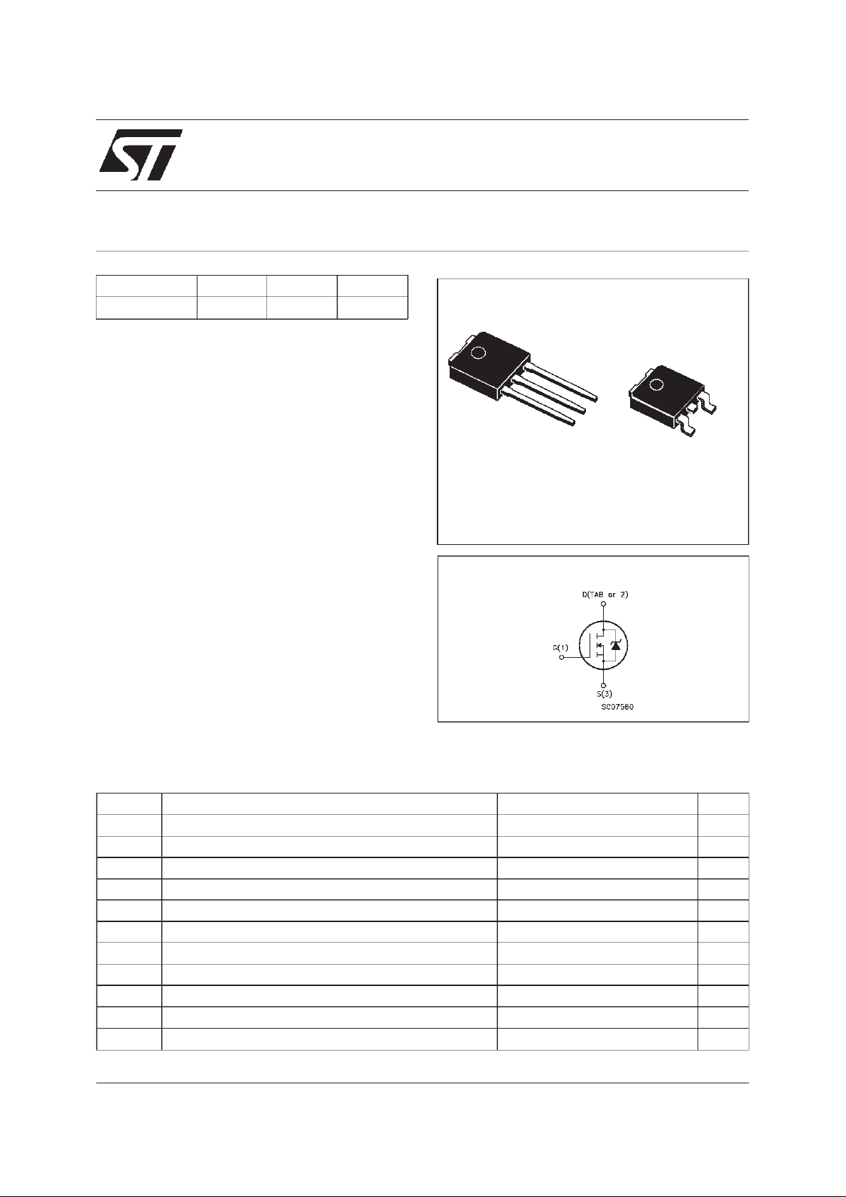
■ THROUG-HOLEIPAK (TO-251) POWER
PACKAGEIN TUBE(SUFFIX ”-1”)
■ SURFACE-MOUNTING DPAK (TO-252)
POWERPACKAGEIN TAPE& REEL
(SUFFIX”T4”)
DESCRIPTION
This Power MOSFET is the latest development of
SGS-THOMSON unique ”Single Feature Size”
strip-based process.The resulting transistor
shows extremely high packing density for low onresistance, rugged avalanche characteristics and
less critical alignment steps therefore a remarkable manufacturingreproducibility.
APPLICATIONS
■ DC MOTOR CONTROL (DISK DRIVERS,etc.)
■ DC-DC& DC-ACCONVERTERS
■ SYNCHRONOUSRECTIFICATION
3
2
IPAK
TO-251
(Suffix”-1”)
1
(Suffix ”T4”)
1
DPAK
TO-252
INTERNAL SCHEMATIC DIAGRAM
3
ABSOLUTE MAXIMUM RATINGS
Symb o l Para meter Value Uni t
V
V
V
I
DM
P
dv/ dt (
T
(•) Pulse width limitedby safe operating area (1)ISD≤ 16 A,di/dt ≤ 200 A/µs, VDD≤ V
July 1998
Drain-source Volt age (VGS=0) 100 V
DS
DGR Drain- gate Voltage (R
Gat e- sourc e V o lt age ± 20 V
GS
I
Drain C ur rent (con t in uous) at Tc=25oC16A
D
I
Drain C ur rent (con t in uous) at Tc=100oC11A
D
=20kΩ)
GS
100 V
(•) Dra in Current (puls ed ) 64 A
Tot al Dis sipati on at Tc=25oC50W
tot
Derating Factor 0.33 W/
1) Peak Diode Recovery v o lt age sl ope 7 V/ns
Sto rage Tem pe r ature -65 to 17 5
stg
T
Max. O perating Ju nc tion Tem peratu r e 175
j
(BR)DSS,Tj≤TJMAX
o
C
o
C
o
C
1/9
Page 2
STD16NE10
THERMAL DATA
R
thj-case
Rthj- a mb
R
thc-sin k
T
AVALANCHE CHARACTERISTICS
Symbol Para met e r Max Valu e Uni t
I
AR
E
Ther mal Resist ance Junction-ca s e Max
Ther mal Resist ance Junction-am bient Max
Ther mal Resist ance Case-si nk T yp
Maximum Lead Tempera t ure F o r S oldering Pur p ose
l
Avalanch e Curre nt , R epetit i v e o r Not- Re petit ive
(pulse w idth limited b y T
Single Pulse Avalanche Energy
AS
(starting T
=25oC, ID=IAR,VDD=30V)
j
max, δ <1%)
j
3.0
100
1.5
275
16 A
75 mJ
o
C/W
oC/W
o
C/W
o
C
ELECTRICAL CHARACTERISTICS (T
=25oC unlessotherwisespecified)
case
OFF
Symbol Parameter Test C ondition s Min. Typ. Max. Unit
V
(BR)DSS
Drain-sou rc e
=250µAVGS=0
I
D
100 V
Breakdown Voltage
I
DSS
I
GSS
Zer o G at e Voltage
Drain Cur rent (V
GS
Gat e-body Le ak a ge
Current (V
DS
=0)
=0)
=MaxRating
V
DS
V
=MaxRating Tc=125
DS
o
C
= ± 20 V
V
GS
1
10
± 100 nA
ON (∗)
Symbol Parameter Test C ondition s Min. Typ. Max. Unit
V
GS(th )
Gate Threshold
V
DS=VGSID
=250µA
234V
Voltage
R
DS(on)
Stati c Drain-so urce O n
VGS=10V ID=8A 0.07 0.1 Ω
Resistance
I
D(on)
On S tate D rain Cur rent VDS>I
D(on)xRDS(on)max
16 A
VGS=10V
DYNAMIC
Symbol Parameter Test C ondition s Min. Typ. Max. Unit
g
(∗)Forward
fs
Tr anscond uctance
C
C
C
Input Ca pac i t an c e
iss
Out put C apacitanc e
oss
Reverse T ransfer
rss
Capa cit an c e
VDS>I
D(on)xRDS(on)maxID
=8 A 5 S
VDS=25V f=1MHz VGS= 0 1600
180
50
2100
250
70
µA
µA
pF
pF
pF
2/9
Page 3
STD16NE10
ELECTRICAL CHARACTERISTICS (continued)
SWITCHINGON
Symbol Parameter Test C ondition s Min. Typ. Max. Unit
t
d(on)
Turn-on Tim e
r
Rise T ime
t
VDD=50V ID=10A
=4.7 Ω VGS=10V
R
G
17
37
(see test circuit, figure 3)
Q
Q
Q
Total Gate Charge
g
Gat e-Sou r ce Charge
gs
Gate-Drain Charge
gd
VDD=80V ID=20A VGS=10V 38
10
12
SWITCHINGOFF
Symbol Parameter Test C ondition s Min. Typ. Max. Unit
t
r(Voff)
t
t
Of f - voltag e Ris e Tim e
Fall Time
f
Cross-over T ime
c
VDD=80V ID=20A
=4.7 Ω VGS=10V
R
G
(see test circuit, figure 5)
11
18
32
SOURCE DRAIN DIODE
Symbol Parameter Test C ondition s Min. Typ. Max. Unit
I
SD
I
SDM
V
SD
t
Q
I
RRM
(∗) Pulsed: Pulse duration =300 µs, duty cycle1.5 %
(•) Pulse width limited by safe operating area
Source-drain Cu rrent
(•)
Source-drain Cu rrent
(pulsed)
(∗) For ward On V o lt age ISD=16A VGS=0 1.5 V
Reverse R ec ov er y
rr
Time
Reverse R ec ov er y
rr
= 20 A di/dt = 100 A /µs
I
SD
=50V Tj=150oC
V
DD
(see test circuit, figure 5)
110
440
Charge
Reverse R ec ov er y
8
Current
23
50
50 nC
15
25
44
16
64
ns
ns
nC
nC
ns
ns
ns
A
A
ns
µC
A
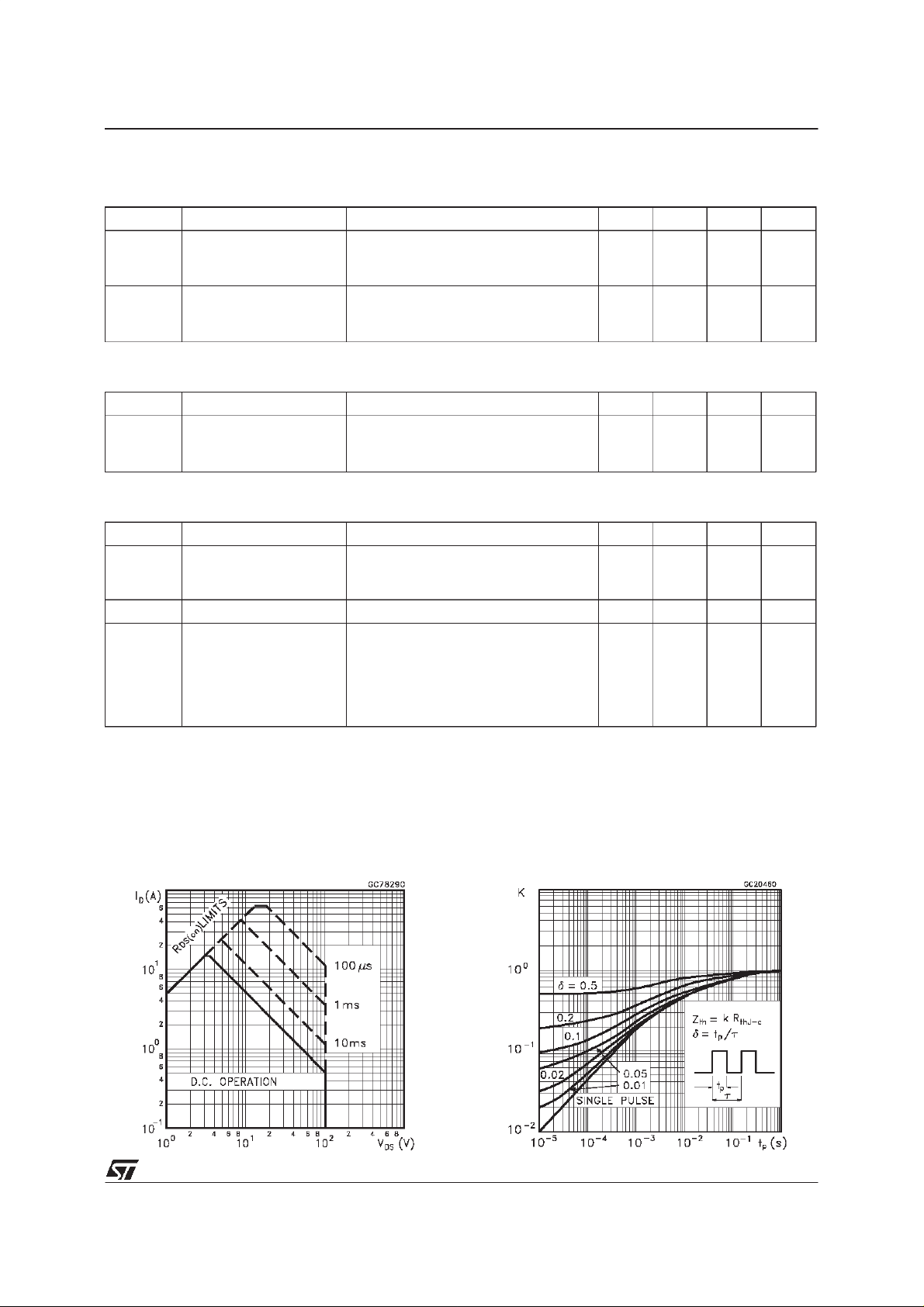
Safe Operating Area ThermalImpedance
3/9
Page 4

STD16NE10
OutputCharacteristics
Transconductance
TransferCharacteristics
StaticDrain-sourceOn Resistance
GateCharge vs Gate-sourceVoltage
4/9
CapacitanceVariations
Page 5

STD16NE10
Normalized GateThresholdVoltage vs
Temperature
Source-drainDiode Forward Characteristics
Normalized On Resistancevs Temperature
5/9
Page 6

STD16NE10
Fig. 1: Unclamped InductiveLoad Test Circuit
Fig. 3: SwitchingTimes Test CircuitsFor
ResistiveLoad
Fig. 2: Unclamped Inductive Waveform
Fig. 4: Gate Chargetest Circuit
Fig. 5: Test Circuit For InductiveLoad Switching
And Diode RecoveryTimes
6/9
Page 7

TO-251 (IPAK) MECHANICAL DATA
STD16NE10
DIM.
mm inch
MIN. TYP. MAX. MIN. TYP. MAX.
A 2.2 2.4 0.086 0.094
A1 0.9 1.1 0.035 0.043
A3 0.7 1.3 0.027 0.051
B 0.64 0.9 0.025 0.031
B2 5.2 5.4 0.204 0.212
B3 0.85 0.033
B5 0.3 0.012
B6 0.95 0.037
C 0.45 0.6 0.017 0.023
C2 0.48 0.6 0.019 0.023
D 6 6.2 0.236 0.244
E 6.4 6.6 0.252 0.260
G 4.4 4.6 0.173 0.181
H 15.9 16.3 0.626 0.641
L 9 9.4 0.354 0.370
L1 0.8 1.2 0.031 0.047
L2 0.8 1 0.031 0.039
A
E
==
C2
L2
B2
==
H
C
A3
A1
B6
L
B
B5
G
==
D
B3
2
13
L1
0068771-E
7/9
Page 8

STD16NE10
TO-252 (DPAK) MECHANICALDATA
DIM.
mm inch
MIN. TYP. MAX. MIN. TYP. MAX.
A 2.2 2.4 0.086 0.094
A1 0.9 1.1 0.035 0.043
A2 0.03 0.23 0.001 0.009
B 0.64 0.9 0.025 0.035
B2 5.2 5.4 0.204 0.212
C 0.45 0.6 0.017 0.023
C2 0.48 0.6 0.019 0.023
D 6 6.2 0.236 0.244
E 6.4 6.6 0.252 0.260
G 4.4 4.6 0.173 0.181
H 9.35 10.1 0.368 0.397
L2 0.8 0.031
L4 0.6 1 0.023 0.039
8/9
H
A
E
==
C2
L2
B2
==
DETAIL”A”
D
2
13
L4
A1
C
A2
DETAIL”A”
B
G
==
0068772-B
Page 9

STD16NE10
Information furnished is believed tobe accurate and reliable. However,STMicroelectronicsassumes no responsibility for theconsequences
of use of such information nor for any infringement of patents or other rights of third parties which may result from its use. No license is
granted by implication orotherwise under any patent orpatent rights of STMicroelectronics. Specification mentioned in this publication are
subject tochange withoutnotice. This publication supersedes andreplaces allinformation previously supplied.STMicroelectronics products
are not authorized for use as critical components in lifesupport devices orsystems withoutexpress written approval of STMicroelectronics.
Australia -Brazil - Canada- China - France- Germany- Italy- Japan- Korea- Malaysia - Malta - Mexico- Morocco- TheNetherlands -
Singapore- Spain- Sweden- Switzerland- Taiwan -Thailand - United Kingdom- U.S.A.
The ST logo isa trademarkof STMicroelectronics
1998 STMicroelectronics– Printed in Italy – AllRightsReserved
STMicroelectronicsGROUP OF COMPANIES
.
9/9
 Loading...