

Page 1

STD16NE06
N - CHANNEL 60V - 0.07Ω - 16A DPAK/IPAK
STripFET POWER MOSFET
TYPE V
DSS
R
DS(on)
I
D
ST D16N E 06 60 V < 0.085 Ω 16 A
■ TYPICALR
■ EXCEPTIONALdv/dtCAPABILITY
■ 100%AVALANCHETESTED
■ APPLICATIONORIENTED
DS(on)
= 0.07 Ω
CHARACTERIZATION
■ THROUG-HOLEIPAK(TO-251) POWER
PACKAGEIN TUBE(SUFFIX ”-1”)
■ SURFACE-MOUNTINGDPAK (TO-252)
POWERPACKAGEIN TAPE& REEL
(SUFFIX”T4”)
DESCRIPTION
This PowerMOSFET is the latest developmentof
STMicroelectronicsunique ”STripFET” strip-ba-
sed process.The resulting transistorshows extremely high packing density for low on-resistance,
rugged avalanche characteristics and less critical
alignmentsteps therefore a remarkablemanufacturingreproducibility.
APPLICATIONS
■ SOLENOIDAND RELAY DRIVERS
■ MOTORCONTROL, AUDIOAMPLIFIERS
■ DC-DCCONVERTERS
■ AUTOMOTIVEENVIRONMENT
3
2
IPAK
TO-251
(Suffix”-1”)
1
(Suffix ”T4”)
1
DPAK
TO-252
INTERNAL SCHEMATIC DIAGRAM
3
ABSOLUTE MAXIMUM RATINGS
Symbol Parameter Value Unit
V
V
V
I
DM
P
dv/ dt Peak Diode Recovery voltage slope 7 V/ ns
T
(•) Pulsewidth limitedby safeoperating area (1)ISD≤ 16 A, di/dt ≤ 300 A/µs, VDD≤ V
February 2000
Dra in- sour c e Volt age (VGS=0) 60 V
DS
Dra in- gat e Voltage (RGS=20kΩ)60V
DGR
Gat e-source Volt age ± 20 V
GS
I
Dra in Cu rr ent ( continuous) a t Tc=25oC16A
D
I
Dra in Cu rr ent ( continuous) a t Tc=100oC11A
D
(•) Dra in Cu rr ent ( p uls ed ) 64 A
Tot al Dis sipation at Tc=25oC40W
tot
Der ati ng Fact or 0.26 W/
St orage T em pe r ature -65 to 175
stg
T
Max. Operating Junct ion Temperatur e 175
j
(BR)DSS,Tj≤TJMAX
o
C
o
C
o
C
1/9
Page 2

STD16NE06
THERMAL DATA
R
thj-case
Rthj-amb
R
thc-sink
T
AVALANCHE CHARACTERISTICS
Symbol Parameter Max Value Unit
I
AR
E
Ther mal Resistanc e Junct ion-case Max
Ther mal Resistanc e Junct ion-ambient Max
Ther mal Resistanc e Case-sink Ty p
Maximum L ead Tem pe ra t ure For Soldering Purpose
l
Avalanche Current, R epetitive or Not-Repetitive
(pulse width limited by T
Single Pul se Avalanche E ner gy
AS
(starting T
=25oC, ID=IAR,VDD=35V)
j
max,δ <1%)
j
3.75
100
1.5
275
16 A
60 mJ
o
C/W
oC/W
o
C/W
o
C
ELECTRICAL CHARACTERISTICS
=25oC unless otherwisespecified)
(T
case
OFF
Symbol Parameter Test Condit ions Min. Typ. Max. Unit
V
(BR)DSS
Drain-source
ID=250µAVGS=0 60 V
Break dow n Vo lt age
I
DSS
I
GSS
Zero Gate Voltage
Drain Curre nt (V
GS
Gat e- bod y Leakag e
Current (V
DS
=0)
=0)
V
=MaxRating
DS
=MaxRating Tc= 125oC
V
DS
V
=± 20 V
GS
1
10
100 nA
±
ON(∗)
Symbol Parameter Test Condit ions Min. Typ. Max. Unit
V
GS(th)
R
DS(on)
Gate Thresho ld Voltage VDS=VGSID= 250 µ A 234V
Sta t ic Drain-s our c e On
VGS=10V ID= 8 A 0.07 0.085
Resistance
I
D(on)
On State Drain Current VDS>I
D(on)xRDS(on)max
16 A
VGS=10V
DYNAMIC
Symbol Parameter Test Condit ions Min. Typ. Max. Unit
g
(∗)Forward
fs
Tr ansc on duc tance
C
C
C
Input Capaci t ance
iss
Out put Capac itance
oss
Reverse Transfer
rss
Capacit a nc e
VDS>I
D(on)xRDS(on)maxID
=8 A 5 9 S
VDS=25V f=1MHz VGS= 0 900
125
35
1200
170
50
µ
µA
Ω
pF
pF
pF
A
2/9
Page 3
STD16NE06
ELECTRICAL CHARACTERISTICS
(continued)
SWITCHING ON
Symbol Parameter Test Condit ions Min. Typ. Max. Unit
t
d(on)
t
r
Turn-on Time
Rise Time
VDD=30V ID=10A
R
G
=4.7
Ω
VGS=10V
20
45
30
60
(see test circuit, figure 3)
Q
Q
Q
Tot al Gate Char ge
g
Gat e- Source Charge
gs
Gate-Drain Charge
gd
VDD=48V ID=16A VGS=10V 25
9.7
6.2
35 nC
SWITCHING OFF
Symbol Parameter Test Condit ions Min. Typ. Max. Unit
t
r(Voff)
t
t
Off-voltage Rise Time
Fall T ime
f
Cross-over Tim e
c
VDD=48V ID=10A
=4.7 Ω VGS=10V
R
G
(see test circuit, figure 5)
25
38
8
11
34
50
SOURCEDRAINDIODE
Symbol Parameter Test Condit ions Min. Typ. Max. Unit
I
SD
I
SDM
V
SD
t
Q
I
RRM
(∗) Pulsed:Pulse duration = 300µs, duty cycle 1.5%
(•) Pulse width limited by safeoperating area
Source-drain Current
(•)
Source-drain Current
16
64
(pulsed)
(∗)ForwardOnVoltage ISD=16A VGS=0 1.5 V
Reverse Recovery
rr
Time
Reverse Recovery
rr
ISD= 16 A di/ dt = 100 A /µs
=30V Tj= 150oC
V
DD
(see test circuit, figure 5)
50
115
Charge
Reverse Recovery
4.5
Current
ns
ns
nC
nC
ns
ns
ns
A
A
ns
nC
A
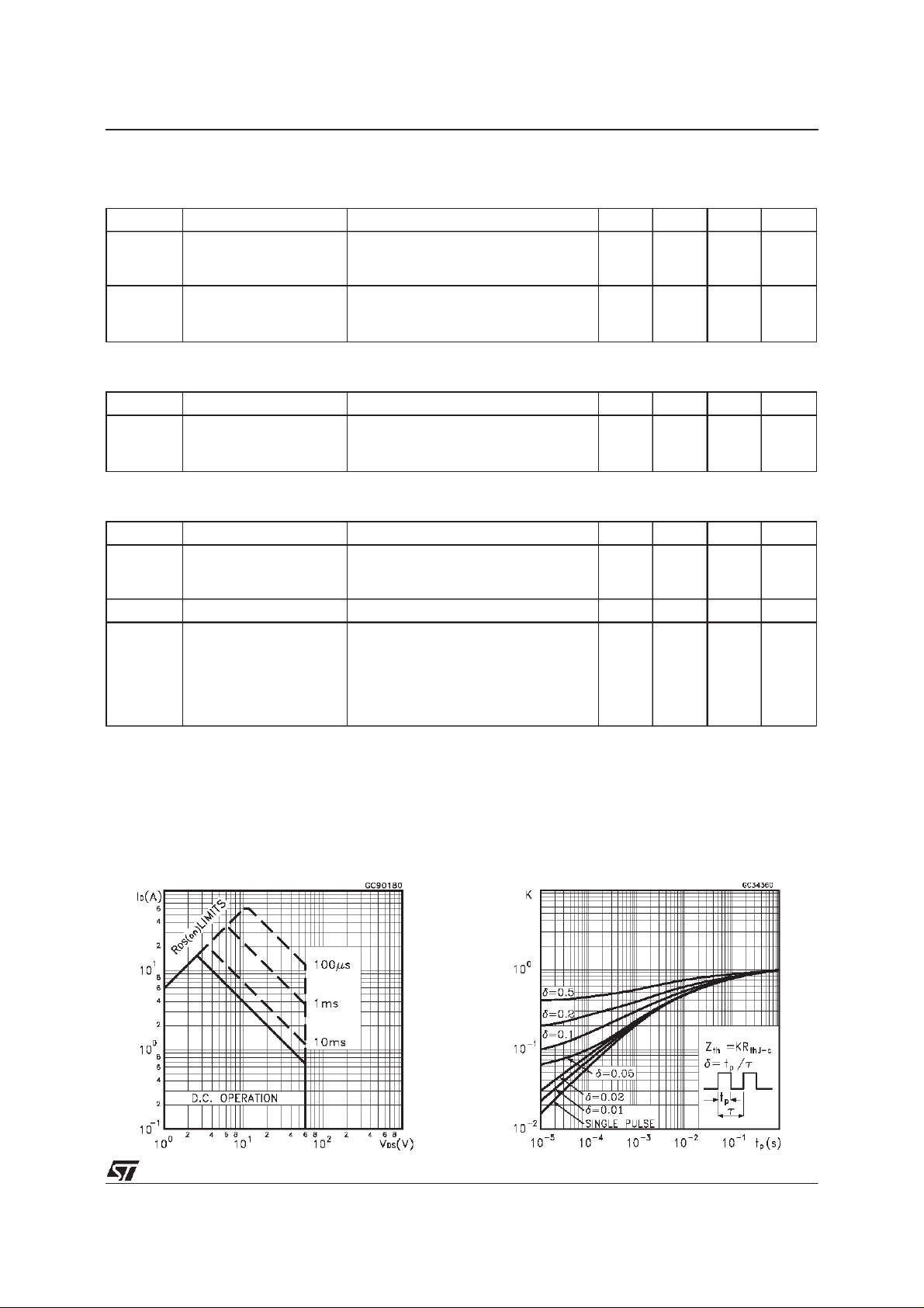
SafeOperating Area ThermalImpedance
3/9
Page 4

STD16NE06
OutputCharacteristics
Transconductance
TransferCharacteristics
Static Drain-sourceOn Resistance
Gate Charge vs Gate-sourceVoltage
4/9
CapacitanceVariations
Page 5

STD16NE06
NormalizedGate ThresholdVoltage vs
Temperature
Source-drainDiode Forward Characteristics
NormalizedOn Resistancevs Temperature
5/9
Page 6

STD16NE06
Fig. 1:
UnclampedInductiveLoad TestCircuit
Fig. 3: SwitchingTimes Test CircuitsFor
ResistiveLoad
Fig. 2:
UnclampedInductive Waveform
Fig. 4: Gate Chargetest Circuit
Fig. 5:
Test Circuit For InductiveLoad Switching
And Diode Recovery Times
6/9
Page 7

TO-251 (IPAK) MECHANICALDATA
STD16NE06
DIM.
mm inch
MIN. TYP. MAX. MIN. TYP. MAX.
A 2.2 2.4 0.086 0.094
A1 0.9 1.1 0.035 0.043
A3 0.7 1.3 0.027 0.051
B 0.64 0.9 0.025 0.031
B2 5.2 5.4 0.204 0.212
B3 0.85 0.033
B5 0.3 0.012
B6 0.95 0.037
C 0.45 0.6 0.017 0.023
C2 0.48 0.6 0.019 0.023
D 6 6.2 0.236 0.244
E 6.4 6.6 0.252 0.260
G 4.4 4.6 0.173 0.181
H 15.9 16.3 0.626 0.641
L 9 9.4 0.354 0.370
L1 0.8 1.2 0.031 0.047
L2 0.8 1 0.031 0.039
A
E
==
C2
L2
B2
==
H
C
A3
A1
B6
L
B
B5
G
==
D
B3
2
13
L1
0068771-E
7/9
Page 8

STD16NE06
TO-252 (DPAK) MECHANICAL DATA
DIM.
mm inch
MIN. TYP. MAX. MIN. TYP. MAX.
A 2.2 2.4 0.086 0.094
A1 0.9 1.1 0.035 0.043
A2 0.03 0.23 0.001 0.009
B 0.64 0.9 0.025 0.035
B2 5.2 5.4 0.204 0.212
C 0.45 0.6 0.017 0.023
C2 0.48 0.6 0.019 0.023
D 6 6.2 0.236 0.244
E 6.4 6.6 0.252 0.260
G 4.4 4.6 0.173 0.181
H 9.35 10.1 0.368 0.397
L2 0.8 0.031
L4 0.6 1 0.023 0.039
8/9
H
A
E
==
C2
L2
B2
==
DETAIL”A”
D
2
13
L4
A1
C
A2
DETAIL”A”
B
G
==
0068772-B
Page 9

STD16NE06
Information furnished is believed to beaccurate and reliable. However, STMicroelectronics assumesno responsibilityforthe consequences
of use of such information nor for any infringement of patents or other rights of third parties which may result from its use. No license is
granted by implication orotherwise under any patent or patent rights of STMicroelectronics. Specificationmentioned in this publicationare
subjectto change without notice.Thispublication supersedes and replacesall information previouslysupplied.STMicroelectronicsproducts
are not authorizedfor use as critical components in life support devices or systems without express written approval of STMicroelectronics.
The STlogo is a trademark ofSTMicroelectronics
1999STMicroelectronics – Printedin Italy – All Rights Reserved
STMicroelectronics GROUP OF COMPANIES
Australia - Brazil - China - Finland - France - Germany - Hong Kong - India - Italy - Japan - Malaysia - Malta - Morocco -
Singapore - Spain - Sweden- Switzerland - United Kingdom - U.S.A.
http://www.st.com
.
9/9
 Loading...