

Page 1
STD12NF06
N-CHANNEL 60V - 0.08 Ω - 12A IPAK/DPAK
STripFET™ II POWER MOSFET
TYPE
V
DSS
STD12NF06 60 V <0.1
■ TYPICAL R
■ EXCEPTIONA L dv/d t CAPABILITY
■ LOW GATE CHARGE
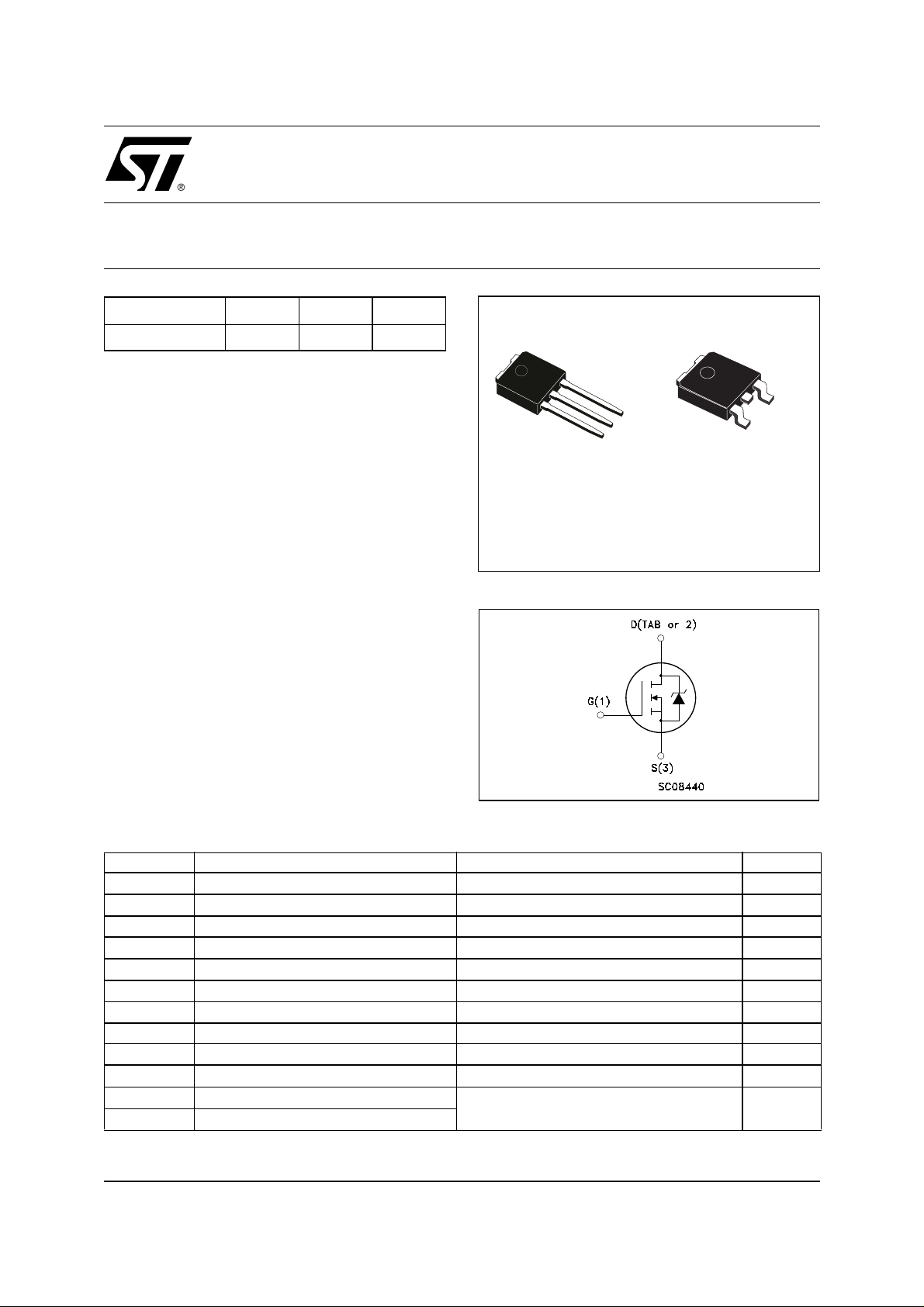
■ THROUGH-HOLE IPAK (TO-251) POWER
(on) = 0.08Ω
DS
R
DS(on)
I
D
Ω
12 A
PACKAGE IN TUBE (SUFFIX “- 1 ")
■ SURFACE-MOUNTING DPAK (TO-252)
POWER PACKAGE IN TAPE & REEL
(SUFFIX “T4")
DESCRIPTION
This Power MOSFET is the latest development of
STMicroelectron is unique "Single Feature Size™" str ipbased process . The res ulting tran sistor sho ws extrem ely
high packing density for low on-resistance, rugged
avalanche characteristics and less critical alignment
steps therefore a remarkable manufacturing
reproducibility.
APPLICATIONS
■ HIGH CURRENT, HIGH SWITCHING SPEED
■ MOTOR CONTROL , AUDIO AMPLIFIERS
■ SOLENOID AND RELAY DRIVERS
■ DC-DC & DC-AC CONVERTERS
■ AUTOMOTIVE ENVIRONMENT
3
2
1
IPAK
TO-251
(Suffix “-1”)
DPAK
TO-252
(Suffix “T4”)
INTERNAL SCHEMATIC DIAGRAM
3
1
ABSOLUTE MAXIMUM RATINGS
Symbol Parameter Value Unit
V
DS
V
DGR
V
GS
I
D
I
D
(
I
DM
P
tot
dv/dt
E
AS
T
stg
T
j
(
Pulse width l i mited by safe operating area. (1) ISD ≤12A, di/dt ≤200A/ µ s , VDD ≤ V
•)
.
Drain-source Voltage (VGS = 0)
Drain-gate Voltage (RGS = 20 kΩ)
60 V
60 V
Gate- source Voltage ± 20 V
Drain Current (continuos) at TC = 25°C
Drain Current (continuos) at TC = 100°C
•)
Drain Current (pulsed) 48 A
Total Dissipation at TC = 25°C
12 A
8.5 A
30 W
Derating Factor 0.2 W/°C
(1)
Peak Diode Recovery voltage slope 15 V/ns
(2)
Single Pulse Avalanche Energy 140 mJ
Storage Temperature
Max. Operating Junction Temperature
(2) Starting Tj = 25 oC, ID = 6A, VDD = 30V
-55 to 175 °C
(BR)DSS
, Tj ≤ T
JMAX
1/10December 2001
Page 2
STD12NF06
THERMA L D ATA
Rthj-case
Rthj-amb
T
Thermal Resistance Junction-case
Thermal Resistance Junction-ambient
Maximum Lead Temperature For Soldering Purpose
l
Max
Max
Typ
5
100
275
°C/W
°C/W
°C
ELECTRICAL CHARACTERISTICS (T
= 25 °C unless otherwise specified)
case
OFF
Symbol Parameter Test Conditions Min. Typ. Max. Unit
I
V
(BR)DSS
Drain-source
= 250 µA, VGS = 0
D
60 V
Breakdown Voltage
V
= Max Rating
DS
V
= Max Rating TC = 100°C
DS
V
= ± 20 V
GS
1
10
±100 nA
ON
(*)
I
DSS
I
GSS
Zero Gate Voltage
Drain Current (V
GS
Gate-body Leakage
Current (V
DS
= 0)
= 0)
Symbol Parameter Test Conditions Min. Typ. Max. Unit
V
V
GS(th)
R
DS(on)
Gate Threshold Voltage
Static Drain-source On
Resistance
= VGS I
DS
V
= 10 V ID = 6 A
GS
= 250 µA
D
234V
0.08 0.1
DYNAMIC
Symbol Parameter Test Conditions Min. Typ. Max. Unit
(*)
g
fs
C
iss
C
oss
C
rss
Forward Transconductance
Input Capacitance
Output Capacitance
Reverse Transfer
Capacitance
V
= 15 V ID=6 A
DS
= 25V, f = 1 MHz, VGS = 0
V
DS
5S
315
70
30
µA
µA
Ω
pF
pF
pF
2/10
Page 3
STD12NF06
ELECTRICAL CHARACTERISTICS (continued)
SWITCHING ON
Symbol Parameter Test Conditions Min. Typ. Max. Unit
= 30 V ID = 6 A
t
d(on)
Turn-on Delay Time
t
r
Rise Time
V
DD
R
= 4.7 Ω VGS = 10 V
G
(Resistive Load, Figure 3)
Q
g
Q
gs
Q
gd
Total Gate Charge
Gate-Source Charge
Gate-Drain Charge
= 48V ID = 12A VGS= 10V
V
DD
SWITCHING OFF
Symbol Parameter Test Conditions Min. Typ. Max. Unit
= 30 V ID = 6 A
t
d(off)
Turn-off Delay Time
t
f
Fall Time
V
DD
R
= 4.7Ω, V
G
GS
= 10 V
(Resistive Load, Figure 3)
SOURCE DRAIN DIODE
Symbol Parameter Test Conditions Min. Typ. Max. Unit
I
SD
I
SDM
V
SD
t
rr
Q
rr
I
RRM
(*)
Pulsed: P ul se duration = 300 µs, duty cycle 1.5 %.
(
•)Pulse width limited by s afe operating area.
Source-drain Current
(•)
Source-drain Current (pulsed)
(*)
Forward On Voltage
Reverse Recovery Time
Reverse Recovery Charge
Reverse Recovery Current
I
= 12 A VGS = 0
SD
= 12 A di/dt = 100A/µs
I
SD
V
= 30 V Tj = 150°C
DD
(see test circuit, Figure 5)
7
18
10
3.0
3.5
17
6
50
65
3.5
12 nC
12
48
1.3 V
ns
ns
nC
nC
ns
ns
A
A
ns
µ
A
C
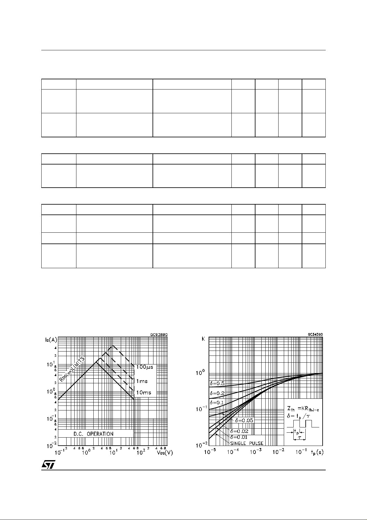
Safe Operating Area
Thermal Impedance
3/10
Page 4

STD12NF06
Output Characteristics Transfer Characteristics
Transconductance Static Drain-source On Resistance
Gate Charge vs Gate-source Voltage Capacitance Variations
4/10
Page 5

STD12NF06
Normalized Gate Threshold Voltage vs Temperature Normalized on Resistance vs Temperature
Source-drain Diode Forward Characteristics Normalized Breakdown Voltage vs Temperature
. .
5/10
Page 6

STD12NF06
Fig. 1: Unclamped Inductive Load Test CircuitFig. 1: Unclamped Inductive Load Test Circuit Fig. 2: Unclamped Inductive Waveform
Fig. 3: Switching Times Test Circuits For Resistive
Load
Fig. 5: Test Circuit For Inductive Load Switching
And Diode Recovery Times
Fig. 4: Gate Charge test Circuit
6/10
Page 7

TO-251 (IPAK) MECHANI CAL DAT A
STD12NF06
DIM.
mm inch
MIN. TYP. MAX. MIN. TYP. MAX.
A 2.2 2.4 0.086 0.094
A1 0.9 1.1 0.035 0.043
A3 0.7 1.3 0.027 0.051
B 0.64 0.9 0.025 0.031
B2 5.2 5.4 0.204 0.212
B3 0.85 0.033
B5 0.3 0.012
B6 0.95 0.037
C 0.45 0.6 0.017 0.023
C2 0.48 0.6 0.019 0.023
D 6 6.2 0.236 0.244
E 6.4 6.6 0.252 0.260
G 4.4 4.6 0.173 0.181
H 15.9 16.3 0.626 0.641
L 9 9.4 0.354 0.370
L1 0.8 1.2 0.031 0.047
L2 0.8 1 0.031 0.039
A
C2
L2
E
B2
= =
= =
H
C
A3
A1
B6
L
B
B5
G
= =
D
B3
2
1 3
L1
0068771-E
7/10
Page 8

STD12NF06
TO-252 (DPAK) MECHANICAL DATA
DIM.
mm inch
MIN. TYP. MAX. MIN. TYP. MAX.
A 2.2 2.4 0.086 0.094
A1 0.9 1.1 0.035 0.043
A2 0.03 0.23 0.001 0.009
B 0.64 0.9 0.025 0.035
B2 5.2 5.4 0.204 0.212
C 0.45 0.6 0.017 0.023
C2 0.48 0.6 0.019 0.023
D 6 6.2 0.236 0.244
E 6.4 6.6 0.252 0.260
G 4.4 4.6 0.173 0.181
H 9.35 10.1 0.368 0.397
L2 0.8 0.031
L4 0.6 1 0.023 0.039
A
C2
L2
E
B2
==
H
DETAIL "A"
D
==
C
B
2
1 3
L4
A1
G
==
A2
DETAIL "A"
0068772-B
8/10
Page 9

STD12NF06
*on sales ty pe
9/10
Page 10

STD12NF06
Information furnished is believed to be accurate and reliable. However, STMicroelectronics assumes no responsibility for the consequences
of use of such information nor for any infringement of patents or other rights of third parties which may result from its use. No license is granted
by implic ation or otherwise under any patent or p atent right s of STMicroelectr oni cs. Spec i fications mentioned i n this publication are s ubj ect
to change without notice. This publication supersedes and replaces all information previously supplied. STMicroelectronics products are not
authorized for use as cri tical comp onents in life support dev i ces or systems wi thout express written approval of STMicroel ectronics.
The ST logo is registered trademark of STMicroelectronics
2001 STMi croelectronics - All Ri ghts Rese rved
All other na m es are the prop erty of their respectiv e owners.
Australi a - Brazil - Canada - Chin a - F i nl and - Franc e - Germany - H ong Kong - Ind ia - Is rael - Italy - Japan - Malaysia - Malta - Morocco -
Singap ore - Spain - Sw eden - Switze rl and - Unit ed K i ngdom - United States .
STMicroelectronics GROUP OF COMPANIES
http:// www.st.com
10/10
 Loading...