

Page 1
STD12NE06L
N - CHANNEL 60V - 0.09Ω - 12A TO-251/TO-252
STripFET POWER MOSFET
TYPE V
DSS
R
DS(on)
I
D
ST D12N E 06L 60 V < 0 . 12 Ω 12 A
■ TYPICALR
■ EXCEPTIONAL dv/dt CAPABILITY
■ AVALANCHERUGGEDTECHNOLOGY
■ 100 % AVALANCHETESTED
■ APPLICATIONORIENTED
DS(on)
= 0.09 Ω
CHARACTERIZATION
■ ADDSUFFIX ”T4” FORORDERING IN TAPE
& REEL
DESCRIPTION
This Power MOSFET is the latest developmentof
STMicroelectronics unique ”Single Feature
Size” strip-based process. The resulting transi-
stor shows extremelyhigh packing density forlow
on-resistance, rugged avalanche characteristics
and less critical alignment steps therefore a remarkablemanufacturingreproducibility.
APPLICATIONS
■ DC MOTOR CONTROL(DISK DRIVES,etc.)
■ DC-DC& DC-AC CONVERTERS
■ SYNCHRONOUSRECTIFICATION
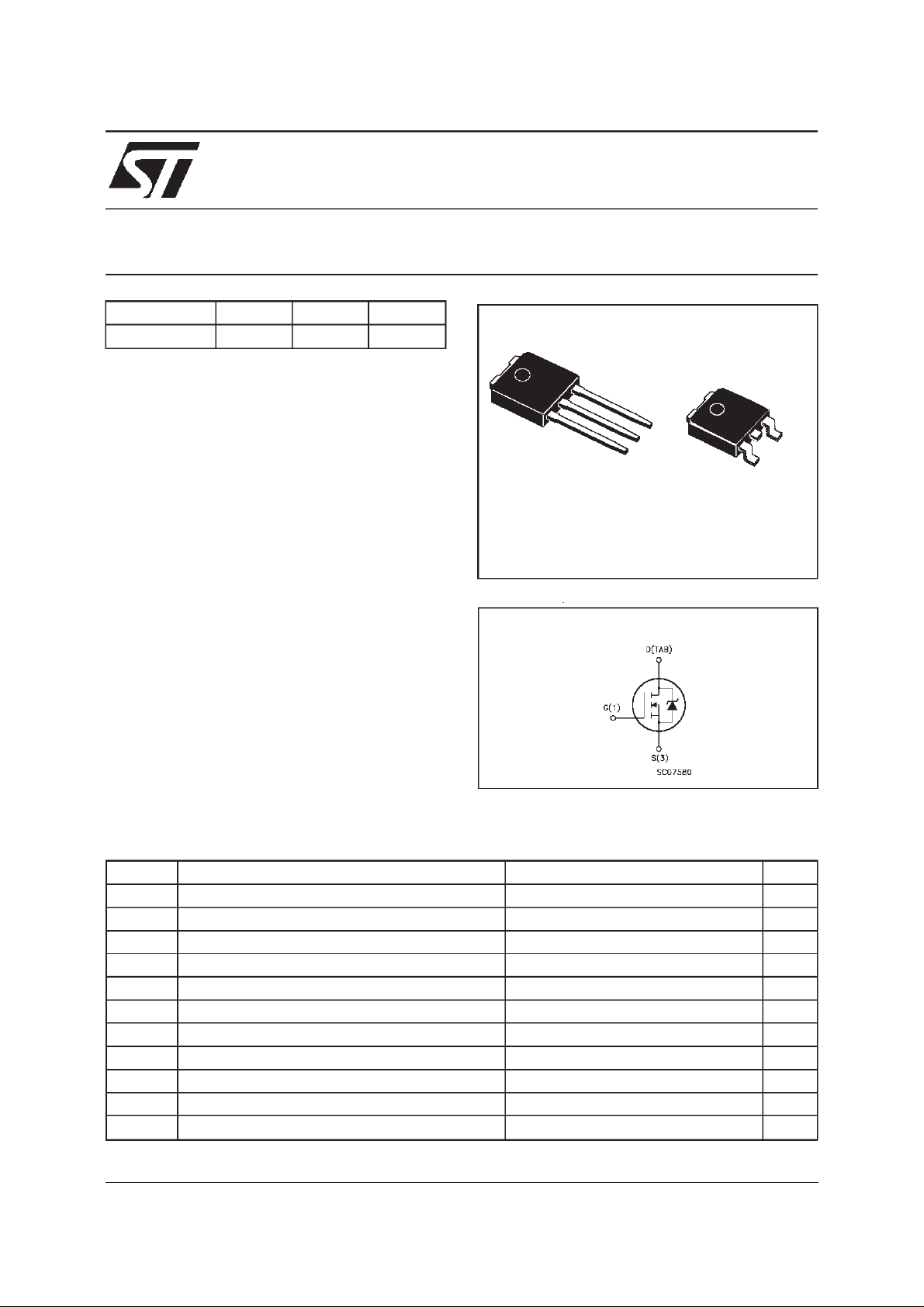
3
2
IPAK
TO-251
(Suffix”-1”)
1
(Suffix”T4”)
1
DPAK
TO-252
INTERNAL SCHEMATIC DIAGRAM
3
ABSOLUTE MAXIMUM RATINGS
Symbol Parameter Value Uni t
V
V
V
I
DM
P
dv/ dt (
T
(•) Pulse width limited by safe operating area (1)ISD≤ 12 A, di/dt ≤ 200 A/µs,VDD≤ V
January 2000
Drain-source Voltage (VGS=0) 60 V
DS
Drain- g at e Voltage (RGS=20kΩ)60V
DGR
Gate-source Voltage ± 20 V
GS
I
Drain Cur rent (c ont in uous ) at Tc=25oC12A
D
I
Drain Cur rent (c ont in uous ) at Tc=100oC8A
D
(•) Drain Current (pulsed) 48 A
Total Dissipation at Tc=25oC35W
tot
Derat ing F ac tor 0.23 W/
1 ) Pea k Diode Recov er y volt a ge slope 6 V/ ns
Sto rage Temperat ure -65 to 175
stg
T
Max. Operating Junct ion Tempe r at ure 175
j
(BR)DSS,Tj≤TJMAX
o
C
o
C
o
C
1/9
Page 2
STD12NE06L
THERMAL DATA
R
thj-case
R
thj-amb
R
thc-sink
T
AVALANCHE CHARACTERISTICS
Symbol Parameter Max Value Unit
I
AR
E
Ther mal Resistanc e Junct ion-case Max
Ther mal Resistanc e Junct ion-ambient Max
Ther mal Resistanc e Case-sink Ty p
Maximum Lead Temperatu r e For Soldering Purpose
l
Avalanche Current, Repetitive or Not-Repetitive
(pulse width limited by T
Single Pul se Avalanc he Ener gy
AS
(starting T
=25oC, ID=IAR,VDD=25V)
j
max)
j
4.3
100
1.5
275
12 A
45 mJ
o
C/W
o
C/W
o
C/W
o
C
ELECTRICAL CHARACTERISTICS
=25oC unless otherwisespecified)
(T
case
OFF
Symbol Parameter Test Condit ions Min. Typ. Max. Unit
V
(BR)DSS
Drain-source
ID=250µAVGS=0 60 V
Break dow n Vo lt age
I
DSS
I
GSS
Zero Gate Voltage
Drain Curre nt (V
GS
Gat e- bod y Leakag e
Current (V
DS
=0)
=0)
V
=MaxRating
DS
=MaxRating Tc= 100oC
V
DS
V
=± 20 V
GS
1
10
100 nA
±
ON(∗)
Symbol Parameter Test Condit ions Min. Typ. Max. Unit
V
GS(th)
R
DS(on)
I
D(on)
Gate Threshold Voltage VDS=VGSID= 250 µA11.72.5V
Sta t ic Drain-s our c e On
Resistance
VGS=5V ID=6A
=10V ID=6A
V
GS
On State Drain Current VDS>I
D(on)xRDS(on )max
0.09
0.07
12 A
0.12
0.10
VGS=10V
DYNAMIC
Symbol Parameter Test Condit ions Min. Typ. Max. Unit
g
(∗)Forward
fs
Tr ansc on duc tance
C
C
C
Input Capaci t ance
iss
Out put Capac itance
oss
Reverse Transfer
rss
Capacit a nc e
VDS>I
D(on)xRDS(on )maxID
=6 A 4 7 S
VDS=25V f=1MHz VGS= 0 700
100
30
1000
140
45
µ
µA
Ω
Ω
pF
pF
pF
A
2/9
Page 3
STD12NE06L
ELECTRICAL CHARACTERISTICS
(continued)
SWITCHING ON
Symbol Parameter Test Condit ions Min. Typ. Max. Unit
t
d(on)
t
r
Turn-on Time
Rise Time
VDD=30V ID=8A
R
=4.7
G
Ω
VGS=5V
17
38
25
50
(see test circuit, figure 3)
Q
Q
Q
Tot al Gate Charge
g
Gat e- Source Charge
gs
Gate-Drain Charge
gd
VDD=48V ID=16A VGS=5V 12
6
6
16 nC
SWITCHING OFF
Symbol Parameter Test Condit ions Min. Typ. Max. Unit
t
r(Voff)
t
t
Off-volt age Rise Time
Fall T ime
f
Cross-over Tim e
c
VDD=48V ID=16A
=4.7 Ω VGS=5V
R
G
(see test circuit, figure 5)
18
30
9
12
25
45
SOURCEDRAINDIODE
Symbol Parameter Test Condit ions Min. Typ. Max. Unit
I
SD
I
SDM
V
SD
t
Q
I
RRM
(∗) Pulsed: Pulse duration = 300µs, duty cycle 1.5%
(•) Pulse width limited by safe operating area
Source-drain Current
(•)
Source-drain Current
12
48
(pulsed)
(∗)ForwardOnVoltage ISD=12A VGS=0 1.5 V
Reverse Recovery
rr
Time
Reverse Recovery
rr
ISD= 16 A di/dt = 100 A/µs
=25V Tj= 150oC
V
DD
(see test circuit, figure 5)
70
0.13
Charge
Reverse Recovery
4
Current
ns
ns
nC
nC
ns
ns
ns
A
A
ns
µ
A
C
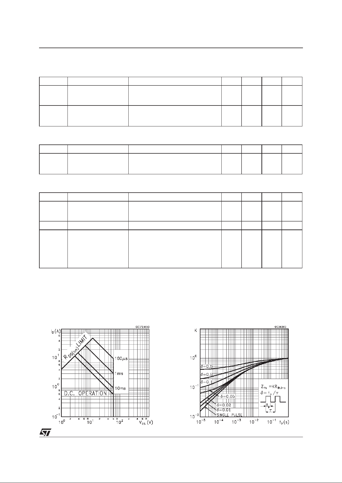
SafeOperating Area for ThermalImpedance
3/9
Page 4

STD12NE06L
OutputCharacteristics
Transconductance
TransferCharacteristics
Static Drain-sourceOn Resistance
Gate Charge vs Gate-sourceVoltage
4/9
CapacitanceVariations
Page 5

STD12NE06L
NormalizedGate ThresholdVoltage vs
Temperature
Source-drainDiode ForwardCharacteristics
NormalizedOn Resistancevs Temperature
5/9
Page 6

STD12NE06L
Fig. 1:
UnclampedInductiveLoad TestCircuit
Fig. 3: SwitchingTimes Test Circuits For
ResistiveLoad
Fig. 2:
UnclampedInductiveWaveform
Fig. 4: GateCharge test Circuit
Fig. 5:
Test CircuitFor InductiveLoad Switching
And Diode Recovery Times
6/9
Page 7

TO-251 (IPAK) MECHANICAL DATA
STD12NE06L
DIM.
mm inch
MIN. TYP. MAX. MIN. TYP. MAX.
A 2.2 2.4 0.086 0.094
A1 0.9 1.1 0.035 0.043
A3 0.7 1.3 0.027 0.051
B 0.64 0.9 0.025 0.031
B2 5.2 5.4 0.204 0.212
B3 0.85 0.033
B5 0.3 0.012
B6 0.95 0.037
C 0.45 0.6 0.017 0.023
C2 0.48 0.6 0.019 0.023
D 6 6.2 0.236 0.244
E 6.4 6.6 0.252 0.260
G 4.4 4.6 0.173 0.181
H 15.9 16.3 0.626 0.641
L 9 9.4 0.354 0.370
L1 0.8 1.2 0.031 0.047
L2 0.8 1 0.031 0.039
A
E
==
C2
L2
B2
==
H
C
A3
A1
B6
L
B
B5
G
==
D
B3
2
13
L1
0068771-E
7/9
Page 8

STD12NE06L
TO-252 (DPAK) MECHANICAL DATA
DIM.
mm inch
MIN. TYP. MAX. MIN. TYP. MAX.
A 2.2 2.4 0.086 0.094
A1 0.9 1.1 0.035 0.043
A2 0.03 0.23 0.001 0.009
B 0.64 0.9 0.025 0.035
B2 5.2 5.4 0.204 0.212
C 0.45 0.6 0.017 0.023
C2 0.48 0.6 0.019 0.023
D 6 6.2 0.236 0.244
E 6.4 6.6 0.252 0.260
G 4.4 4.6 0.173 0.181
H 9.35 10.1 0.368 0.397
L2 0.8 0.031
L4 0.6 1 0.023 0.039
8/9
H
A
E
==
C2
L2
B2
==
DETAIL”A”
D
2
13
L4
A1
C
A2
DETAIL”A”
B
G
==
0068772-B
Page 9

STD12NE06L
Information furnishedis believedtobeaccurateand reliable.However, STMicroelectronics assumes no responsibilityfor the consequences
of use of such information nor for any infringement of patents or other rights of third parties which may result from its use. No license is
granted by implication or otherwise under anypatent or patent rights ofSTMicroelectronics. Specificationmentioned in this publicationare
subjecttochange withoutnotice.This publication supersedes andreplaces all informationpreviously supplied.STMicroelectronics products
are not authorized for use as critical components in lifesupportdevices or systems without express written approval of STMicroelectronics.
The ST logo is a trademark of STMicroelectronics
1999 STMicroelectronics – Printed in Italy – All Rights Reserved
STMicroelectronics GROUP OF COMPANIES
Australia - Brazil - China - Finland - France - Germany - Hong Kong - India - Italy- Japan - Malaysia - Malta - Morocco -
Singapore - Spain - Sweden - Switzerland - United Kingdom - U.S.A.
http://www.st.com
.
9/9
 Loading...