

Page 1
STD12N10L
N - CHANNEL 100V - 0.12 Ω - 12A TO-252
LOW THRESHOLD POWER MOS TRANSISTOR
TYPE V
DSS
R
DS(o n)
I
D
ST D12N 10L 100 V < 0.15 Ω 12 A
■ TYPICALR
■ AVALANCHERUGGEDTECHNOLOGY
■ 100%AVALANCHETESTED
■ HIGHCURRENT CAPABILITY
■ 175
■ LOW THRESHOLDDRIVE
■ FORTHROUGH-HOLE VERSION CONTACT
o
C OPERATINGTEMPERATURE
DS(on)
= 0.12 Ω
SALESOFFICE
APPLICATIONS
■ HIGHCURRENT, HIGH SPEEDSWITCHING
■ SOLENOIDAND RELAYDRIVERS
■ MOTORCONTROL, AUDIOAMPLIFIERS
■ DC-DC& DC-AC CONVERTERS
■ AUTOMOTIVE ENVIRONMENT(INJECTION,
ABS, AIR-BG, LAMPDRIVERS,Etc.)
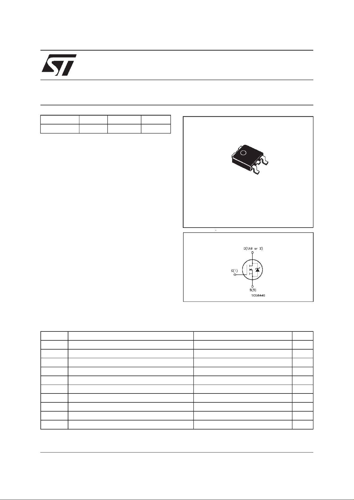
3
1
DPAK
TO-252
(Suffix ”T4”)
INTERNAL SCHEMATIC DIAGRAM
ABSOLUTE MAXIMUM RATINGS
Symbol Parameter Value Uni t
V
V
V
I
DM
P
T
(•) Pulse width limited by safe operating area
November 1999
Drain-source Voltage (VGS= 0) 100 V
DS
Drain- g at e Voltage (RGS=20kΩ) 100 V
DGR
Gate-source Voltage
GS
I
Drain Cur rent (c ont in uous ) at Tc=25oC12A
D
I
Drain Cur rent (c ont in uous ) at Tc=100oC8A
D
15 V
±
(•) Drain Current (pulsed) 48 A
Total Dissipation at Tc=25oC50W
tot
Derat ing F ac tor 0.33 W/
Sto rage Temperat ure -65 to 175
stg
T
Max. Operating Junction Tem pe r at ur e 175
j
o
C
o
C
o
C
1/9
Page 2

STD12N10L
THERMAL DATA
R
thj-case
R
thj-amb
R
thc-sink
T
Ther mal Resistanc e Junct ion-case Max
Ther mal Resistanc e Junct ion-ambient Max
Ther mal Resistanc e Case-sink Ty p
Maximum Lead Te m perature For Soldering Purpos e
l
3
100
1.5
275
o
C/W
o
C/W
o
C/W
o
C
ELECTRICAL CHARACTERISTICS
=25oC unless otherwisespecified)
(T
case
OFF
Symbol Parameter Test Conditions Min. Typ. Max. Unit
V
(BR)DSS
Drain-source
ID=250µAVGS= 0 100 V
Break dow n Vo lt age
I
DSS
I
GSS
Zero Gate Voltage
Drain Curre nt (V
GS
Gat e- bod y Leakag e
Current (V
DS
=0)
=0)
V
=MaxRating
DS
=MaxRating Tc= 125oC
V
DS
V
= ± 15 V ± 100 nA
GS
1
10
ON(∗)
Symbol Parameter Test Conditions Min. Typ. Max. Unit
V
GS(th)
R
DS(on)
I
D(on)
Gate Threshold Voltage VDS=VGSID= 250 µA11.62.5V
Sta t ic Drain-s our c e On
Resistance
VGS=10V ID=6A
=5V ID=6A
V
GS
On State Drain Current VDS>I
D(on)xRDS(on )max
0.12
0.17
12 A
0.15
0.2
VGS=10V
DYNAMIC
Symbol Parameter Test Conditions Min. Typ. Max. Unit
g
(∗)Forward
fs
Tr ansc on duc tance
C
C
C
Input Capaci t ance
iss
Out put Capac itance
oss
Reverse Transfer
rss
Capacit a nc e
VDS>I
D(on)xRDS(on )maxID
=6A 6.5 10 S
VDS=25V f=1MHz VGS= 0 800
150
50
µ
µA
Ω
Ω
pF
pF
pF
A
2/9
Page 3

STD12N10L
ELECTRICAL CHARACTERISTICS
(continued)
SWITCHINGON
Symbol Parameter Test Conditions Min. Typ. Max. Unit
t
d(on)
Tur n-on Delay T ime
Rise Time
t
r
VDD=50V ID=6A
R
=4.7
G
Ω
VGS=5V
15
40
(Resis t iv e Load, see fig. 3)
Q
Q
Q
Tot al Gate C har ge
g
Gat e- Source Charge
gs
Gate-Drain Charge
gd
VDD=80V ID=12A VGS=5V 20
6
10
30 nC
SWITCHINGOFF
Symbol Parameter Test Conditions Min. Typ. Max. Unit
t
r(Voff)
t
t
Off-volt age Rise Time
Fall T ime
f
Cross-over Tim e
c
VDD=80V ID=12A
=4.7 Ω VGS=5V
R
G
(Indu ct iv e Load, see fig. 5)
12
12
25
SOURCEDRAINDIODE
Symbol Parameter Test Conditions Min. Typ. Max. Unit
I
V
I
SDM
SD
Q
I
RRM
SD
t
Source-drain Current
(•)
Source-drain Current
12
48
(pulsed)
(∗)ForwardOnVoltage ISD=12A VGS=0 1.5 V
Reverse Recovery
rr
Time
Reverse Recovery
rr
ISD= 12 A di/dt = 100 A/µs
=30V Tj=150oC
V
DD
(see test circuit, fig. 5)
145
580
Charge
Reverse Recovery
8
Current
ns
ns
nC
nC
ns
ns
ns
A
A
ns
µ
A
C
(∗) Pulsed:Pulse duration = 300µs, duty cycle 1.5%
(•) Pulse width limited by safe operating area
3/9
Page 4

STD12N10L
Fig. 1:
UnclampedInductiveLoad TestCircuit
Fig. 3: SwitchingTimes Test Circuits For
ResistiveLoad
Fig. 2:
UnclampedInductiveWaveform
Fig. 4: Gate Chargetest Circuit
Fig. 5:
Test Circuit For InductiveLoad Switching
And Diode Recovery Times
4/9
Page 5

TO-252 (DPAK) MECHANICAL DATA
STD12N10L
DIM.
mm inch
MIN. TYP. MAX. MIN. TYP. MAX.
A 2.2 2.4 0.086 0.094
A1 0.9 1.1 0.035 0.043
A2 0.03 0.23 0.001 0.009
B 0.64 0.9 0.025 0.035
B2 5.2 5.4 0.204 0.212
C 0.45 0.6 0.017 0.023
C2 0.48 0.6 0.019 0.023
D 6 6.2 0.236 0.244
E 6.4 6.6 0.252 0.260
G 4.4 4.6 0.173 0.181
H 9.35 10.1 0.368 0.397
L2 0.8 0.031
L4 0.6 1 0.023 0.039
H
A
E
C2
L2
B2
==
==
DETAIL”A”
D
2
13
L4
A1
C
A2
DETAIL”A”
B
G
==
0068772-B
5/9
Page 6

STD12N10L
Information furnishedis believed to beaccurateand reliable.However, STMicroelectronics assumesno responsibilityfor the consequences
of use of such information nor for any infringement of patents or other rights of third parties which may result from its use. No license is
granted by implication or otherwise under anypatent or patent rights ofSTMicroelectronics. Specificationmentioned in this publication are
subjecttochange withoutnotice.This publication supersedes andreplaces all information previouslysupplied. STMicroelectronics products
are not authorized for use as critical components in life supportdevices or systemswithout express written approval of STMicroelectronics.
The STlogo is a trademark of STMicroelectronics
1999 STMicroelectronics – Printed in Italy – All Rights Reserved
STMicroelectronics GROUP OF COMPANIES
Australia - Brazil - China - Finland - France - Germany - Hong Kong - India - Italy - Japan- Malaysia - Malta - Morocco -
6/9
Singapore - Spain - Sweden- Switzerland - United Kingdom - U.S.A.
http://www.st.com
.
 Loading...