

Page 1
The SP5659 is a single chip frequency synthesiser designed
for tuning systems up to 2·7GHz.
The RF preamplifier drives a divide-by two prescaler which
can be disabled for applications up to 2GHz, allowing direct
interfacing with the programmable divider, resulting in a step
size equal to the comparison frequency. For applications up
to 2·7GHz the divide-by two is enabled to give a step size of
twice the comparison frequency.
The comparison frequency is obtained either from an onchip crystal controlled oscillator or from an external source.
The oscillator frequency F
REF
or the comparison frequency
F
COMP
may be switched to the REF/COMP output; this feature
is ideally suited to providing the reference frequency for a
second synthesiser such as in a double conversion tuner (see
Fig. 5).
The synthesiser is controlled via an I
2
C bus and responds
to one of four programmable addresses which are selected by
applying a specific voltage to the Address input. This feature
enables two or more synthesisers to be used in a system.
The SP5659 contains four switching ports, P0-P3 and a
5-level ADC, the output of which can be read via the I
2
C bus.
The SP5659 also contains a varactor line disable and
charge pump disable facility.
FEATURES
■ Complete 2·7GHz Single Chip System
■ Optimised for Low Phase Noise
■ Selectable 42 prescaler
■ Selectable Reference Division Ratio
■
Selectable Reference/Comparison Frequency Output
■ Selectable Charge Pump Current
■ Varactor Drive Amplifier Disable
■ 5-Level ADC
■ Variable I
2
C BUS Address for Multi-tuner Applications
SP5659
2·7GHz I2C Bus Low Phase Noise Synthesiser
Preliminary Information
Supersedes March 1996 version, DS4206-1.8 DS4296 - 2.0 June 1998
SP5659
1
2
3
4
5
6
7
8
MP16
16
15
14
13
12
11
10
9
CHARGE PUMP
CRYSTAL
REF/COMP
ADDRESS
SDA
SCL
PORT P3
PORT P2
DRIVE
V
EE
RF INPUT
RF INPUT
V
CC
ADC
PORT P0
PORT P1
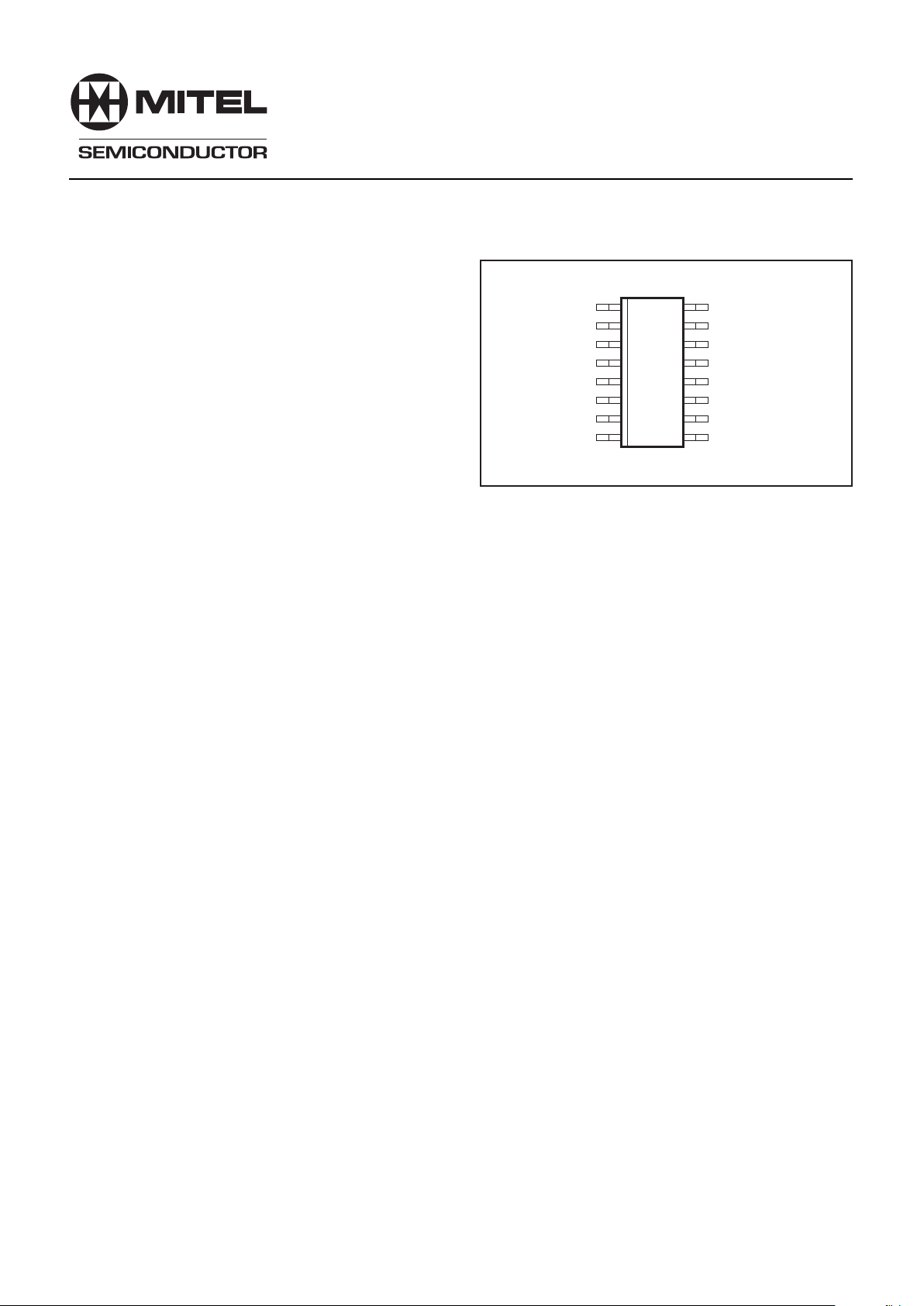
Fig. 1 Pin connections – top view
■ ESD Protection: 4kV, Mil-Std-883C, Method 3015
(1)
■ Pin Compatible with SP5658
(1) Normal ESD handling precautions should be observed.
APPLICATIONS
■ Satellite TV
■ High IF Cable Tuning Systems
THERMAL DATA
u
JC
= 41°C/W
u
JA
= 111°C/W
ORDERING INFORMATION
SP5659 KG/MP1S (Tubes)
SP5659 KG/MP1T (Tape and reel)
Page 2
2
SP5659
ELECTRICAL CHARACTERISTICS
T
AMB
= 220°C to 180°C, V
CC
= 14·5V to 15·5V, reference frequency = 4MHz.
These Characteristics are guaranteed by either production test or design. They apply within the specified ambient temperature
and supply voltage ranges unless otherwise stated.
Supply current, I
CC
RF input voltage
RF input impedance
RF input capacitance
SDA, SCL
Input high voltage
Input low voltage
Input high current
Input low current
Leakage current
Input hysteresis
SDA
Output voltage
Charge Pump
Output current
Output leakage current
Drive output current
Drive saturation voltage
External reference input frequency
External reference input amplitude
Crystal frequency
Crystal oscillator drive level
Recommended crystal series resistance
Crystal oscillator negative resistance
REF/COMP output voltage, enabled
Comparison frequency
Equivalent phase noise at phase detector
RF division ratio
Reference division ratio
P0, P1, P2, P3 sink current
P0, P1, P2, P3 leakage current
ADC input voltage
ADC input current
Address input current high
Address input current low
Typ.
Value
12
13,14
13,14
13,14
5, 6
5, 6
5, 6
5, 6
5, 6
5, 6
5
1
1
16
16
2
2
2
2
2
3
7,8,9,10
11
11
4
4
50
3
0
1
2
200
4
35
10
400
240
480
10
68
58
50
2
0·8
63
350
2142
85
73
300
5·5
1·5
10
210
10
0·4
610
350
200
20
500
16
200
2
131071
262142
10
610
1
20·5
Min. Max.
mA
mA
mVrms
mVrms
mVrms
Ω
pF
V
V
µA
µA
µA
V
V
nA
mA
mV
MHz
mVp-p
MHz
mVp-p
Ω
Ω
mVp-p
MHz
dBC/Hz
mA
µA
µA
mA
mA
V
CC
= 5V, PE = 1 (note 1)
V
CC
= 5V, PE = 0
300MHz to 2·7GHz, PE = 1
(prescaler enabled) see Fig. 4b
100MHz, PE = 1 (prescaler
enabled) see Fig. 4b
100MHz to 2·0GHz, PE = 0
(prescaler disabled) see Fig. 4b
See Fig. 10
See Fig. 10
Input voltage = V
CC
Input voltage = V
EE
VCC = V
EE
Sink current = 3mA
Drive output disabled
AC coupled sinewave
AC coupled sinewave
Parallel resonant crystal (note 2)
Includes temperature and process
tolerances
AC coupled, RE = 1, see note 3
See note 4
Prescaler disabled, see Table 1
Prescaler enabled, see Table 1
See Table 1
V
PORT
= 0·7V
V
PORT
= 13·2V
See Fig. 3 Table 5
V
CC >VINPUT >VEE
Input voltage = V
CC
Input voltage = V
EE
Characteristic Pin Units Conditions
NOTES
1. Maximum power consumption is 468mW with V
CC
= 5·5V and all ports off.
2. Resistance specified is maximum under all conditions including start up.
3. If the REF/COMP output is not used, it should be left open circuit or connected to V
CC
and disabled by setting RE to logic 0.
4. 6kHz loop bandwidth, phase comparator frequency 250kHZ. Figure measured at 1kHz offset DSB (within loop bandwidth).
Page 3
3
SP5659
Supply voltage
RF input voltage
RF input DC offset
Port voltage
Total port current
ADC input DC offset
REF/COMP output DC offset
Charge pump DC offset
Drive DC offset
Crystal oscillator DC offset
Address DC offset
SDA, SCL input voltage
Storage temperature
Junction temperature
Port in off state
Port in on state
12
13,14
13, 14
7-10
7-10
7-10
11
3
1
16
2
4
5, 6
ABSOLUTE MAXIMUM RATINGS
All voltages are referred to VEE at 0V
Max.Min.
7
2·5
V
CC
10·3
14
6
50
V
CC
10·3
VCC10·3
V
CC
10·3
V
CC
10·3
VCC10·3
V
CC
10·3
6
1150
1150
Value
20·3
20·3
20·3
20·3
20·3
20·3
20·3
20·3
20·3
20·3
255
V
V p-p
V
V
V
mA
V
V
V
V
V
V
V
°C
°C
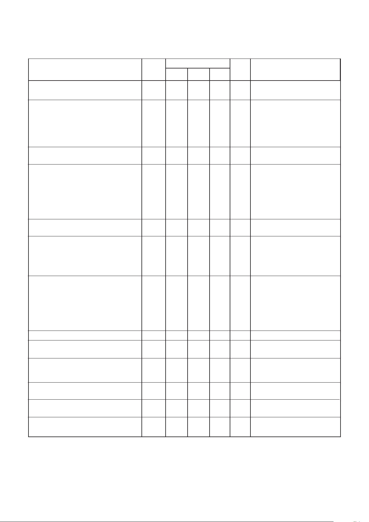
Fig. 2 Block diagram
RF IN
ADDRESS
SDA
LOCK
DET
42/1
13
14
4
5
F
COMP
CHARGE
PUMP
CRYSTAL
2
OSC
789
10
P3 P2 P1 P0
F
PD
416/17
4-BIT
COUNT
13-BIT
COUNT
PROGRAMMABLE DIVIDER
PREAMP
17-BIT LATCH
DIVIDE RATIO
1-BIT
COUNT
PE
PHASE
COMP
I2C
TRANSCEIVER
SCL
6
CHARGE
PUMP
2-BIT
LATCH
FPD/2
3-BIT ADC
ADC
11
3
POWER ON
DETECT
4-BIT LATCH
AND
PORT INTERFACE
REFERENCE
DIVIDER
(SEE TABLE 1)
REF/COMP
3
2-BIT
LATCH
V
CC
V
EE
15
C1, C0
F
L
F
REF
5-BIT LATCH AND
MODE CONTROL LOGIC
(SEE TABLE 6)
DISABLE
DRIVE
16
1
MODE
CONTROL
P0 TEST
CONTROL
12
Parameter Pin Units Conditions
Page 4

4
SP5659
FUNCTIONAL DESCRIPTION
The SP5659 contains all the elements necessary – with
the exception of a frequency reference, loop filter and external
high voltage transistor – to control a varactor tuned local
oscillator, so forming a complete PLL frequency synthesised
source. The device allows for operation with a high comparison
frequency and is fabricated in high speed logic which enables
the generation of a loop with good phase noise performance.
The block diagram is shown in Fig. 2.
The RF input signal is fed to an internal preamplifier, which
provides gain and reverse isolation from the divider signals.
The output of the preamplifier interfaces with a 17-bit fully
programmable divider via a 42 prescaler. For applications up
to 2·0GHz RF input, the prescaler can be disabled, so
eliminating the degradation in phase noise due to prescaler
action. The divider is of MN1A architecture, where N = 16 or
17, the M counter is 13 bits and the A counter is 4 bits.
The output of the programmable divider, F
PD
, is fed to the
phase comparator where it is compared in phase and frequency
domains with the comparison frequency F
COMP
. This frequency
is derived either from the on-chip crystal controlled oscillator
or from an external reference source. In either case, the
reference frequency F
REF
is divided down to the comparison
frequency by the reference divider, which is programmable to
one of 15 ratios as detailed in Table 1.
The output of the phase detector feeds a charge pump and
loop amplifier section which, when used with an external high
voltage transistor and loop filter, integrates the current pulses
into the varactor line voltage. By invoking the device test
modes as described in Fig. 3, Table 6, the varactor drive
output can be disabled, so switching the external transistor
off. This allows an external voltage to be applied to the
varactor line for tuner alignment purposes. Similarly, the
charge can also be disabled to a high impedance state.
The programmable divider output F
PD
/2 can be switched to
port P0 by programming the device into test mode as set out
in Table 6.
PROGRAMMING
The SP5659 is controlled by an I2C Bus. Data and Clock
are fed in on the SDA and SCL lines respectively, as defined
by the I
2
C Bus format. The synthesiser can either accept new
data (write mode) or send data (read mode). The LSB of the
address byte (R/W) sets the device into write mode if it is low
and read mode if it is high. Tables 1 and 2 in Fig. 3 illustrate
the format of the data. The device can be programmed to
respond to several addresses, which enables the use of more
than one synthesiser in an I
2
C Bus system. Table 4 in Fig. 3
shows how the address is selected by applying a voltage to
the address input.
When the device receives a valid address byte, it pulls the
SDA line low during the acknowledge period, and during
following acknowledge periods after further data bytes are
programmed. When the device is programmed into the read
mode, the controller accepting the data must pull the SDA line
low during all status byte acknowledge periods to read another status byte. If the controller fails to pull the SDA line low
during this period, the device generates an internal STOP
condition, which inhibits further reading.
WRITE Mode (Frequency Synthesis)
With reference to Table 2, bytes 2 and 3 contain frequency
information bits 214 to 20 inclusive. Auxiliary frequency bits 2
16
and 215 are in byte 4. For most frequencies, only bytes 2 and
3 will be required. The remainder of byte 4 and byte 5 control
the prescaler enable, reference divider ratio (see Fig. 3),
output ports and test modes (see Table 6).
After reception and acknowledgment of a valid address
(byte 1), the first bit of the following byte determines whether
the byte is interpreted as byte 2 (logic ‘0’) or byte 4 (logic ‘1’);
the next data byte is then interpreted as byte 3 or byte 5,
respectively. After two complete data bytes have been received, additional data bytes can be entered, where byte
interpretation follows the same procedure without readdressing the device. This procedure continues until a STOP condition is received. The STOP condition can be generated after
any data byte; if, however, it occurs during a byte transmission then the previous data is retained.
To facilitate smooth fine tuning, the frequency data bytes are
only accepted by the device after all 17 bits of the data have
been received or after the generation of a STOP condition.
Repeatedly sending bytes 2 and 3 only will not change the
frequency. A frequency change when one of the following
data sequences is sent to an addressed device:
Bytes 2, 3, 4, 5
Bytes 4, 5, 2, 3
or when a STOP condition follows valid data bytes thus:
Bytes 2, 3, 4, STOP
Bytes 4, 5, 2, STOP
Bytes 2, 3, STOP
Bytes 2, STOP
Bytes 4, STOP
It should be noted that the SP5569 must be addressed
initially with both frequency AND control byte data, since the
control byte contains reference divider information which
must be provided before a chosen frequency can be synthesised. This implies that after initial turn on, bytes 2, 3 and 4
must be sent followed by a STOP condition as a minimum
requirement. Alternatively, bytes 2, 3, 4 and 5 must be sent if
port information is also required.
READ Mode
When the device is in read mode the status byte read from
the device on the SDA line takes the form shown in Fig. 3,
Table 3.
Bit 1 (POR) is the power-on reset indicator and is set to a
logic ‘1’ if the V
CC
supply to the device has dropped below 3V
(at 25˚C), for example, when the device is initially turned on.
R2
0
0
0
0
1
1
1
1
0
0
0
0
1
1
1
1
R3
0
0
0
0
0
0
0
0
1
1
1
1
1
1
1
1
R1
0
0
1
1
0
0
1
1
0
0
1
1
0
0
1
1
Comparison frequency
2MHz
1MHz
500kHz
250kHz
125kHz
62·5kHz
31·25kHz
15·625kHz
800kHz
400kHz
200kHz
100kHz
50kHz
25kHz
12·5kHz
R0
0
1
0
1
0
1
0
1
0
1
0
1
0
1
0
1
Ratio
2
4
8
16
32
64
128
256
Invalid
5
10
20
40
80
160
320
Table 1 Reference division ratios (4MHz external reference)
Page 5

5
SP5659
The POR is reset to 0 when the read sequence is terminated
by a STOP command. When POR is set high (at low V
CC
), the
programmed information is lost and the output ports are all set
to high impedance.
Bit 2 (FL) indicates whether the device is phase locked, a
logic ‘1’ is present if the device is locked, and a logic ‘0’ if the
device is unlocked.
Bits 6, 7 and 8 (A2, A1, A0) combine to give the output of
the ADC. The ADC can be used to feed AFC information to the
microprocessor via the I
2
C bus.
Additional Programmable Features
Prescaler enable
The 42 prescaler is enabled by setting bit PE in byte 4 to
a logic ‘1’. A logic ‘0’ disables the prescaler, directly passing
the RF input to the 17-bit counter. Bit PE is a static select only.
Charge pump current
The charge pump current can be programmed by bits C1 and
C0 in data byte 5, as defined in Fig. 3, Table 7.
Test mode
The test modes are invoked by setting bit RE to logic ‘0’ and
bit RTS to logic ‘1’ within the programming data and are selected
by bits TS2, TS1 and TS0 as shown in Fig. 3, Table 6. When TS2,
TS1 and TS0 are received, the device retains previously P2, P1
and P0 data.
Reference comparison frequency output
The reference frequency F
REF
can be switched to the REF/
COMP output (pin 3) by setting byte 5 bit RE to logic ‘1’ and bit
RTS to logic ‘0’. The comparison frequency F
COMP
can be
switched to the REF/COMP output by setting bit RE to logic ‘1’
and bit RTS to logic ‘1’. For RE set to logic ‘0’, the output is
disabled and set to a high state. RE and RTS default to logic ‘1’
during power-up, thus enabling F
COMP
at the REF/COMP output.
Table 1 Write data format (MSB transmitted first)
Table 3 Read data format
1
POR
1
A0
Byte 1
Byte 2
Address
Status byte
1FL0X0X0
X
MA0
A1
MA1
A2
A
A
Address input voltage level
0V to 0·1V
CC
Open circuit
0·4VCC to 0·6V
CC
0·9VCC to V
CC
Table 4 ADC levels
MA0
0
1
0
1
MA1
0
0
1
1
Table 5 Address selection
Voltage on ADC input
0·6V
CC
to V
CC
0·45V
CC
to 0·6V
CC
0·3V
CC
to 0·45V
CC
0·15V
CC
to 0·3V
CC
0V to 0·15V
CC
A1
0
1
1
0
0
A2
1
0
0
0
0
A0
0
1
0
1
0
A : Acknowledge bit
MA1, MA0 : Variable address bits (see Table 5)
2
16-20
: Programmable division ratio control bits
PE : Prescaler enable
R3, R2, R1, R0 : Reference division ratio select (see Table 1)
C1, C0 : Charge pump current select (see Table 7)
RE : Reference oscillator output enable
RTS : REF/COMP select when RE = 1, Test mode enable when RE = 0 (see Table 6)
TS2, TS1, TS0 : Test mode control bits (valid when RE = 0 and RTS = 1,see Table 6)
P0 : Port P0 output state (always valid except when RE = 0 and RTS = 1 (see Table 6)
P3, P2, P1 : Ports P2, P1 and P0 output states
POR : Power on reset indicator
FL : Phase lock flag
A2, A1, A0 : ADC data (see Table 4)
X : Don’t care
Address
Programmable divider
Programmable divider
Control data
Control data
MA0
2
9
2
1
R1
P1/TS1
1
2
14
2
6
2
16
C0
0
2
13
2
5
2
15
RE
0
2
12
2
4
PE
RTS
0
2
11
2
3
R3
P3
MSB
1
0
2
7
1
C1
MA1
2
10
2
2
R2
P2/TS2
LSB
0
2
8
2
0
R0
P0/TS0
Byte 1
Byte 2
Byte 3
Byte 4
Byte 5
A
A
A
A
A
Fig. 3 Data formats
cont…
Page 6

6
SP5659
Table 6 REF/COMP output mode and test modes
TS2
X
X
X
X
X
1
X
X
TS1
X
0
0
1
1
X
X
X
TS0
X
0
1
0
1
X
X
X
REF/COMP O/P mode
Disabled to high state
Disabled to high state
Disabled to high state
Disabled to high state
Disabled to high state
Disabled to high state
F
REF
switched
F
COMP
switched
RTS
0
1
1
1
1
1
0
1
RE
0
0
0
0
0
0
1
1
Test mode description
Normal operation
Charge pump sink, status byte FL = 1
Charge pump source, status byte FL = 0
Charge pump disabled, status byte FL = 0
Port P0 = F
PD
/2
Varactor drive output disabled
Normal operation
Normal operation
C1
byte 5, bit 1
0
0
1
1
C0
byte 5, bit 2
0
1
0
1
Min.
690
6195
6416
6900
Current (
µA)
Typ.
6120
6260
6555
61200
Max.
6150
6325
6694
61500
Table 7 Charge pump current
Fig. 3 Data formats (continued)
300
100
100
FREQUENCY (MHz)
V
IN
(mV RMS INTO 50 Ω )
OPERATING
WINDOW
1000 2000 3000
10
40
3500
300
100
100
FREQUENCY (MHz)
V
IN
(mV RMS INTO 50 Ω )
OPERATING
WINDOW
1000 2000 3000
10
40
3500
300 2700
Fig. 4a Prescaler disabled, PE = 0
Fig. 4b Prescaler enabled, PE = 1
Fig. 4 Typical input sensitivity
Page 7
7
SP5659
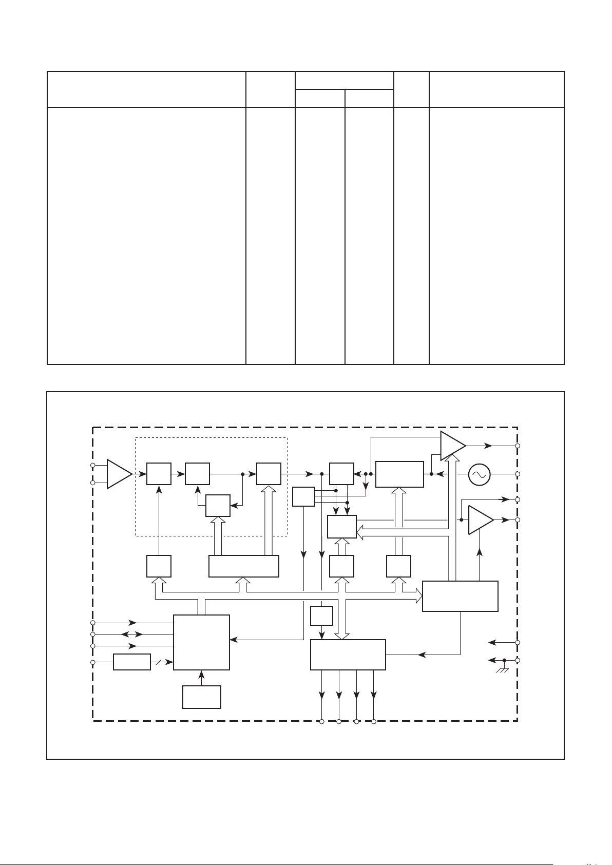
DOUBLE CONVERSION TUNER SYSTEMS
The high 2·7GHz maximum operating frequency and excellent
noise characteristics of the SP5659 allow the construction of
double conversion high IF tuners.
A typical as shown in Fig. 5 uses the SP5659 as the first local
oscillator control for full band up conversion to an IF of greater
than 1GHz. The wide range of reference division ratios allows the
SP5659 to be used for both the up converter local oscillator with
a high phase comparison frequency (hence low phase noise)
and the down converter which uses the device in a lower
comparison frequency mode, which gives a fine step size.
50-900MHz
SP8659SP8659
SP8659SP8659
REFERENCE CLOCK
FIRST LO
SECOND LO
1650-2700MHz
1·6GHz
38·9MHz
Fig. 5 Example of double conversion from VHF/UHF frequencies to TV IF
BCW31
2·2n
47k16k
TUNER
SP5659
1
2
3
4
5
6
7
8
16
15
14
13
12
11
10
9
1n
130V
22k
1n
OSCILLATOR OUTPUT
15V
10n
ADC
P0
P1
112V
68p
13·3k
15n
P3
P2
REF/COMP
10n
CONTROL
MICRO
REF
ADDRESS
SDA
SCL
SP5659
1
2
3
4MHz 18p
Optional application using on-chip
crystal controlled oscillator
Fig. 6 Typical application
APPLICATION NOTES
An application note, AN168, is available for designing with
synthesisers such as the SP5659. It covers aspects such as loop
filter design and decoupling.
The application note is published in the Mitel Semiconductor
Media IC Handbook. A generic test/demonstration board has
been produced, which can be used for the SP5659. A circuit
diagram and layout for the board are shown in Figs. 7 and 8.
The board can be used for the following purposes:
(A) Measuring RF sensitivity performance
(B) Indicating port function
(C) Synthesising a voltage controlled oscillator
(D) Testing external reference sources
The programming codes relevant to these tests are given in
Fig. 3.
Page 8

8
SP5659
1
2
3
4
5
6
7
8
16
15
14
13
12
11
10
9
15V
C10 1n
C4 1n
C5 1n
C3 68p
R6 13·3k
C2
15n
TR1
2N3904
R8 16k R9 47k
C12 2·2n
P3
VAR
GND
C7
100nC8100nC9100n
15V 130V 112V
P2
R8 22k
C13
100p
C14
100p
P1
DISABLE/REF
ENABLE
DATA/SDA
CLOCK/SCL
C1
18p
X1
4MHz
EXTERNAL
REFERENCE
SK2
C6 10n
(NOT FITTED,
SEE NOTE 3)
SK1
RF INPUT
NOTES
1. The circuit diagram shown is designed
for use with a number of synthesisers.
2. The LED connected to pin 11 is
redundant when an SP5659 is used in
this board.
3. To use an external reference,
capacitor C6 must be fitted and
capacitor C1 removed from the board.
R3 4·7k
D3
R2 4·7k
D2
R1 4·7k
D1
R4 4·7kD4R5 4·7k
D5
P4
112V
C11
1n
Fig. 7 Test board circuit diagram
RJM51 BOTTOM SILK SCREEN COMPONENT LOCATION
Fig. 8 Test board layout
Page 9

9
SP5659
LOOP BANDWIDTH
Most applications for which the SP5659 is intended require
a loop filter bandwidth of between 2kHz and 10kHz.
Typically, the VCO phase noise will be specified at both
1kHz and 10kHz offset. It is common practice to arrange the
loop filter bandwidth such that the 1kHz figure lies within the
loop bandwidth. The phase noise therefore depends on the
synthesiser comparator noise floor rather than the VCO
The 10kHz offset figure should depend on the VCO provided
that the loop has been designed correctly and is not
underdamped.
REFERENCE SOURCE
The SP5659 offers optimal local oscillator phase noise
performance when operated with a large step size. This is
because the local oscillator phase noise within the loop
bandwidth is:
F
LO
Phase comparator noise floor 120log
10
F
COMP
where FLO is the local oscillator frequency and F
COMP
is the
phase comparator frequency.
Assuming the phase comparator noise floor is flat regardless
of sampling frequency, this means that the best performance
will be achieved when the overall local oscillator to phase
comparator division ratio is a minimum.
The are two ways of achieving a higher phase comparator
sampling frequency:
1. Reduce the division ratio between the reference source
and the phase comparator
2. Use a higher reference source frequency
The second approach may be preferred for best
performance since it is possible that the noise floor of the
reference oscillator may degrade the phase comparator
performance if the reference division ratio is very small.
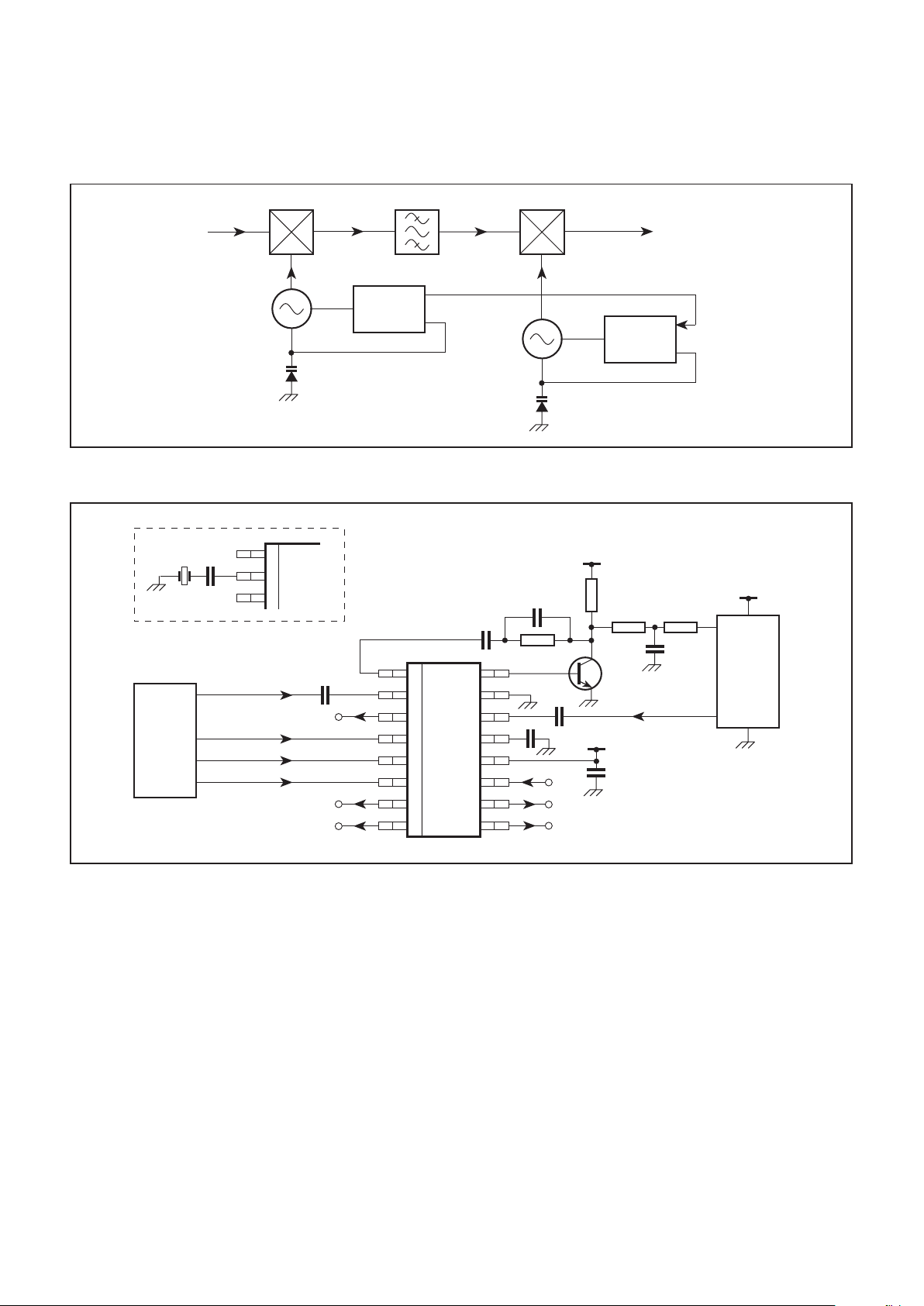
DRIVING TWO SP5659s FROM A COMMON
REFERENCE
The REF/COMP output on pin 3 allows two synthesisers to be
driven from a common reference. To do this, the first device
should be programmed by setting RE = 1 and RTS = 0. The
driven device should be programmed for normal operation with
RE = 0 and RTS = 0. The two devices should be connected as
shown in Fig. 9.
SP5659
1
2
3
4
5
6
7
8
16
15
14
13
12
11
10
9
4MHz 18p
SP5659
1
2
3
4
5
6
7
8
16
15
14
13
12
11
10
9
1n
Fig. 9 Two SP5659 devices using a common reference
Fig. 10 Typical RF input impedance
S
11:ZO
= 50Ω
NORMALISED TO 50Ω
FREQUENCY MARKERS AT 100MHz,
500MHz, 1GHz AND 2·7GHz
j
2
j
1
j
0.5
j
0.2
0
2
j
0.2
2
j
0.5
2
j
1
2
j
2
1
0.5
0.2
j
5
2
j
5
2
5
Page 10

10
SP5659
RF INPUT
500
500
CHARGE
PUMP
RF inputs
Loop amplifier
Reference oscillator
Address input
SDA, SCL and ADC
REF/COMP output
V
CC
3k
30k
10k
ADDRESS
V
CC
V
REF
100
DRIVE
OUTPUT
OS
(O/P DISABLE)
200
SCL/SDA/ADC
3k
ACK
*
*
ON SDA ONLY
V
CC
CRYSTAL
V
CC
V
CC
PORT
REF/COMP
ENABLE/
DISABLE
Output ports
RF INPUT
13
14
16
1
4
3
2
Fig. 11 Input/output interface circuits
Page 11

11
SP5659
Page 12

12
SP5659
PACKAGE DETAILS
Dimensions are shown thus: mm (in).
CUSTOMER SERVICE CENTRES
●
FRANCE & BENELUX Les Ulis Cedex
Tel: (1) 69 18 90 00 Fax: (1) 64 46 06 07
●
GERMANY Munich Tel: (089) 419508-20 Fax: (089) 419508-55
●
ITALY Milan Tel: (02) 6607151 Fax: (02) 66040993
●
JAPAN Tokyo Tel: (03) 5276-5501 Fax: (03) 5276-5510
●
KOREA Seoul Tel: (2) 5668141 Fax: (2) 5697933
●
NORTH AMERICA Scotts Valley, USA
Tel: (408) 438 2900 Fax: (408) 438 5576/6231
This publication is issued to provide information only which (unless agreed by the Company in writing) may not be used, applied or reproduced for any purpose nor form part of any order or contract nor to be regarded
as a representation relating to the products or services concerned. No warranty or guarantee express or implied is made regarding the capability, performance or suitability of any product or service. The Company
reserves the right to alter without prior notice the specification, design or price of any product or service. Information concerning possible methods of use is provided as a guide only and does not constitute any
guarantee that such methods of use will be satisfactory in a specific piece of equipment. It is the user's responsibility to fully determine the performance and suitability of any equipment using such information and
to ensure that any publication or data used is up to date and has not been superseded. These products are not suitable for use in any medical products whose failure to perform may result in significant injury
or death to the user. All products and materials are sold and services provided subject to the Company's conditions of sale, which are available on request.
All brand names and product names used in this publication are trademarks, registered trademarks or trade names of their respective owners.
Internet: http://www.mitelsemi.com
© Mitel 1998 Publication No. DS4206 Issue No. 2.0 June 1998 TECHNICAL DOCUMENTATION – NOT FOR RESALE. PRINTED IN UNITED KINGDOM
●
SOUTH EAST ASIA Singapore
Tel:(65) 333 6193 Fax: (65) 333 6192
●
SWEDEN Stockholm Tel: 46 8 702 97 70 Fax: 46 8 640 47 36
●
TAIWAN, ROC Taipei Tel: 886 2 25461260 Fax: 886 2 27190260
●
UK, EIRE, DENMARK, FINLAND & NORWAY
Swindon Tel: (01793) 726666 Fax : (01793) 518582
These are supported by Agents and Distributors in major countries
worldwide.
0·35/0·49
(0·014/0·019)
3·80/4·00
(0·150/0·157)
5·80/6·20
(0·228/0·244)
9·80/10·01
(0·386/0·394)
16
16-LEAD MINIATURE PLASTIC DIL - MP16
16 LEADS AT
1·27 (0·050)
NOM SPACING
0·69 (0·027)
MAX
0·10/0·25
(0·004/0·010)
1·35/1·91
(0·053/0·075)
SPOT REF.
CHAMFER
REF.
PIN 1
NOTES
1. Controlling dimensions are inches.
2. This package outline diagram is for guidance
only. Please contact your MITEL Customer
Service Centre for further information.
0·25/0·51
(0·010/0·020)
×45°
0·18/0·25
(0·007/0·010)
0-8
°
0·41/1·27
(0·016/0·050)
 Loading...