

Page 1
Si2400
V.22
BIS
ISO
MODEM
™
WITH INTEGRATED
Features
!
Data Modem Formats
"
2400 bps: V.22bis
"
1200 bps: V.22, V.23, Bell 212A
"
300 bps: V.21, Bell 103
"
V.25 Fast Connect and V.23 Reversing
"
SIA and other security protocols
!
Caller ID Detection and Decode
!
DTMF Tone Gen./Detection
!
3.3 V or 5.0 V Power
!
UART with Flow Control
!
Integrated DAA
"
Capacitive Isolation
"
Parallel Phone Detect
"
Globally Compliant Line Interface
"
Overcurrent Protection
!
AT Command Set Support
!
Integrated Voice Codec
!
PCM Data Pass-Through Mode
!
HDLC Framing in Hardware
!
Call Progress Support
Applications
!
Set Top Boxes
!
Power Meters
!
Security Systems
!
ATM Terminals
!
Medical Monitoring
!
Point-of-Sale
Description
The Si2400 ISOmodem™ i s a complete modem chipset with integr ated
direct access arrangement (DAA) that provides a programmable line
interface to meet global te lephon e line r equir emen ts. Available in two 16pin small outline (SOIC) packag es, it eliminates the need for a se parate
DSP data pump, modem controller, analog front end (AFE), isolation
transformer, relays, opto-isolators, 2- to 4-wire hybrid, and voice codec.
The Si2400 is ideal for embedd ed modem applications due to its small
board space, low power consumption, and global compliance.
Functional Block Diagram
Si2400 Si3015
TXD
RXD
RESET
EOFR/GPIO1
AIN/GPIO2
ESC/GPIO3
ALERT/GPIO4
CTS
CLKOUT
XTALI
XTALO
MUX
Control
Interface
Clock
Interface
UART
µ
Controller
(AT Decode r
Call Progress)
DSP
(Data Pump)
Audio
Codec
Hybrid
and
DC
T ermination
Isolation Interface
Isolation Interface
Ring Detect
Off-Hook
RX
FILT
FILT2
REF
DCT
VREG2
REXT
REXT2
RNG1
RNG2
QB
QE
QE2
G
LOBAL
Si2400
Ordering Information
See page 71.
Pin Assignments
Si2400
XTALI
XTALO
CLKOUT
RESET
RNG1
RNG2
Patents pending
V
TXD
RXD
CTS
QE2
DCT
IGND
C1B
QB
QE
1
2
3
4
D
5
6
7
8
Si3015
1
2
3
4
5
6
7
8
DAA
Si3015
EOFR/GPIO1
16
AIN/GPIO2
15
ESC/GPIO3
14
ISOB
13
GND
12
C1A
11
ALERT/GPIO4
10
AOUT
9
FILT2
16
FILT
15
RX
14
REXT
13
REXT2
12
REF
11
VREG2
10
VREG
9
AOUT
Rev. 0.95 4/00 Copyright © 2000 by Silicon Laboratories Si2400-DS095
Page 2

Si2400
2 Rev. 0.95
Page 3

Si2400
T
ABLE OF
C
ONTENTS
Section Page
Electrical Specifications . . . . . . . . . . . . . . . . . . . . . . . . . . . . . . . . . . . . . . . . . . . . . . . . . 4
Typical Application Circuit . . . . . . . . . . . . . . . . . . . . . . . . . . . . . . . . . . . . . . . . . . . . . . . 9
Typical Application Circuit Schematic . . . . . . . . . . . . . . . . . . . . . . . . . . . . . . . . . . . . 9
Bill of Materials . . . . . . . . . . . . . . . . . . . . . . . . . . . . . . . . . . . . . . . . . . . . . . . . . . . . . . 10
Analog Input/Output . . . . . . . . . . . . . . . . . . . . . . . . . . . . . . . . . . . . . . . . . . . . . . . . . . 11
Functional Description . . . . . . . . . . . . . . . . . . . . . . . . . . . . . . . . . . . . . . . . . . . . . . . . . . 12
Digital Interface . . . . . . . . . . . . . . . . . . . . . . . . . . . . . . . . . . . . . . . . . . . . . . . . . . . . . 13
Configurations and Data Rates . . . . . . . . . . . . . . . . . . . . . . . . . . . . . . . . . . . . . . . . . 13
Low Power Modes . . . . . . . . . . . . . . . . . . . . . . . . . . . . . . . . . . . . . . . . . . . . . . . . . . . 14
Global DAA Operation . . . . . . . . . . . . . . . . . . . . . . . . . . . . . . . . . . . . . . . . . . . . . . . . 15
Parallel Phone Detection . . . . . . . . . . . . . . . . . . . . . . . . . . . . . . . . . . . . . . . . . . . . . . 15
Carrier Detect/Loss . . . . . . . . . . . . . . . . . . . . . . . . . . . . . . . . . . . . . . . . . . . . . . . . . . 18
Overcurrent Protection . . . . . . . . . . . . . . . . . . . . . . . . . . . . . . . . . . . . . . . . . . . . . . . . 18
Caller ID Decoding Operation . . . . . . . . . . . . . . . . . . . . . . . . . . . . . . . . . . . . . . . . . . 18
Tone Generation and Tone Detection . . . . . . . . . . . . . . . . . . . . . . . . . . . . . . . . . . . . 19
PCM Data Mode . . . . . . . . . . . . . . . . . . . . . . . . . . . . . . . . . . . . . . . . . . . . . . . . . . . . . 19
Analog Codec . . . . . . . . . . . . . . . . . . . . . . . . . . . . . . . . . . . . . . . . . . . . . . . . . . . . . . . 21
V.23 Operation/V.23 Reversing . . . . . . . . . . . . . . . . . . . . . . . . . . . . . . . . . . . . . . . . . 21
V.42 HDLC Mode . . . . . . . . . . . . . . . . . . . . . . . . . . . . . . . . . . . . . . . . . . . . . . . . . . . . 22
Fast Connect . . . . . . . . . . . . . . . . . . . . . . . . . . . . . . . . . . . . . . . . . . . . . . . . . . . . . . . 23
Clock Generation Subsystem . . . . . . . . . . . . . . . . . . . . . . . . . . . . . . . . . . . . . . . . . . . 23
AT Command Set . . . . . . . . . . . . . . . . . . . . . . . . . . . . . . . . . . . . . . . . . . . . . . . . . . . . . . . 25
Command Line Execution . . . . . . . . . . . . . . . . . . . . . . . . . . . . . . . . . . . . . . . . . . . . . 25
< CR > End Of Line Character . . . . . . . . . . . . . . . . . . . . . . . . . . . . . . . . . . . . . . . . . . 25
AT Command Set Description . . . . . . . . . . . . . . . . . . . . . . . . . . . . . . . . . . . . . . . . . . 25
Extended AT Commands for the Alarm Industry . . . . . . . . . . . . . . . . . . . . . . . . . . . . 27
Modem Result Codes and Call Progress . . . . . . . . . . . . . . . . . . . . . . . . . . . . . . . . . . 30
Low Level DSP Control . . . . . . . . . . . . . . . . . . . . . . . . . . . . . . . . . . . . . . . . . . . . . . . . . . 32
S Registers . . . . . . . . . . . . . . . . . . . . . . . . . . . . . . . . . . . . . . . . . . . . . . . . . . . . . . . . . . . . 35
Appendix A—DAA Operation . . . . . . . . . . . . . . . . . . . . . . . . . . . . . . . . . . . . . . . . . . . . . 62
Appendix B—Typical Modem Applications Examples . . . . . . . . . . . . . . . . . . . . . . . . . 67
Appendix C—UL1950 3rd Edition . . . . . . . . . . . . . . . . . . . . . . . . . . . . . . . . . . . . . . . . . . 68
Ordering Guide . . . . . . . . . . . . . . . . . . . . . . . . . . . . . . . . . . . . . . . . . . . . . . . . . . . . . . . . . 71
Package Outline . . . . . . . . . . . . . . . . . . . . . . . . . . . . . . . . . . . . . . . . . . . . . . . . . . . . . . . . 72
Contact Information . . . . . . . . . . . . . . . . . . . . . . . . . . . . . . . . . . . . . . . . . . . . . . . . . . . . . 76
Rev. 0.95 3
Page 4

Si2400
Electrical Specifications
Table 1. Recommended Operating Conditions
Parameter
1
Ambient Temperature T
Ambient Temperature T
Si2400 Supply Voltage, Digital
Notes:
1. The Si2400 specifications are guaranteed when the typical application circuit (including component tolerance) and any
Si2400 and any Si3015 are used. See Figure3 on page 9 for typical application circuit.
2. All minimum and maximum specifications are guaranteed and apply across the recommended operating conditions.
Typical values apply at nominal supply voltages and an operating temperature of 25 °C unless otherwise stated.
3. The digital supply, V
from 3.3 V. The 3.3V operation applies to both the serial port and the digital signals CTS
.
RESET
3
, can operate from eit her 3.3 V or 5.0 V. The Si 2400 inte rface suppo rts 3.3V logic when operating
D
Symbol Test Condition
A
A
V
D
K-Grade 0 25 70 °C
B-Grade –40 25 85 °C
Min
2
Typ
Max
2
3.0 3.3/5.0 5.25 V
, CLKOUT, GPIO1–4, and
Unit
Table 2. DAA Loop Characteristics
(VD = 3.0 to 3.6 V or 4.75 to 5.25 V, TA = 0 to 70°C
for K-Grade, TA = –40
to 85°C for B-Grade)
Parameter Symbol Test Condition Min Typ Max Unit
DC Termination Voltage V
DC Termination Voltage V
DC Termination Voltage V
DC Termination Voltage V
DC Termination Voltage V
DC Termination Voltage V
DC Termination Voltage V
DC Termination Voltage V
On Hook Leakage Current I
Operating Loop Current I
Operating Loop Current I
TR
TR
TR
TR
TR
TR
TR
TR
LK
LP
LP
DC Ring Current — — 20 µA
Ring Detect Voltage V
Ring Detect Voltage V
Ring Frequency F
RD
RD
R
Ringer Equivalence Number* REN — — 0.2
*Note:C15, R14, Z2, and Z3 not installed.
IL = 20 mA, ACT = 1
——7.5V
DCT = 11 (CTR21)
IL = 42 mA, ACT = 1
— — 14.5 V
DCT = 11 (CTR21)
IL = 50 mA, ACT = 1
——40 V
DCT = 11 (CTR21)
IL = 60 mA, ACT = 1
40 — — V
DCT = 11 (CTR21)
IL = 20 mA, ACT = 0
——6.0V
DCT = 01 (Japan)
IL = 100 mA, ACT = 0
11 — — V
DCT = 01 (Japan)
IL = 20 mA, ACT = 0
——7.5V
DCT = 10 (FCC)
IL = 100 mA, ACT = 0
12 — — V
DCT = 10 (FCC)
V
= –48 V — — 1 µA
BAT
FCC/Japan Modes 13 — 120 mA
CTR21 13 — 60 mA
RT = 0 11 — 22 V
RT = 1 17 — 33 V
15 — 68 Hz
RMS
RMS
4 Rev. 0.95
Page 5
Si2400
Table 3. DC Characteristics
(VD = 4.75 to 5.25 V, TA = 0 to 70°C
Parameter Symbol Test Condition Min Typ Max Unit
for K-Grade, TA = –40
to 85°C for B-Grade)
High Level Input Voltage V
Low Level Input Voltage V
High Level Output Voltage V
Low Level Output Voltage V
Low Level Output Voltage, GPIO1–4 V
Input Leakage Current I
Power Supply Current, Digital* I
Power Supply Current, DSP Power Down* I
Power Supply Current, Wake-On-Ring (ATZ) I
Power Supply Current, Total Power Down I
*Note: Specifications assume MCKR = 0 (default). Typical value is 4 mA lower when MCKR = 1 and 6 mA lower when
MCKR = 2,3.
Measurements are taken with inputs at rails and no loads on outputs.
IH
IL
OH
OL
OL
L
D
D
D
D
IO = –2 mA 2.4 — — V
IO = 2 mA — — 0.4 V
IO = 40 mA — — 0.6 V
VD pin — 28 32 mA
VD pin — 16 19 mA
VD pin — 10 11 mA
VD pin — 60 105 µA
3.5 — — V
——0.8V
–10 — 10 µA
Table 4. DC Characteristics
(VD = 3.0 to 3.6 V, TA = 0 to 70°C
for K-Grade, TA = –40
to 85°C for B-Grade)
Parameter Symbol Test Condition Min Typ Max Unit
High Level Input Voltage V
Low Level Input Voltage V
High Level Output Voltage V
Low Level Output Voltage V
Low Level Output Voltage, GPIO1–4 V
Input Leakage Current I
Power Supply Current, Digital I
Power Supply Current, DSP Power Down I
Power Supply Current, Wake-On-Ring I
Power Supply Current, Total Power Down I
*Note: Specifications assume MCKR = 0 (default). Typical value is 2 mA lower when MCKR = 1 and 3 mA lower when
MCKR = 2,3.
Measurements are taken with inputs at rails and no loads on outputs.
IH
IL
OH
OL
OL
L
D
D
D
D
IO = –2 mA 2.4 — — V
IO = 2 mA — — 0.35 V
IO = 20 mA — — 0.6 V
VD pin — 15 21 mA
VD pin — 9 14 mA
VD pin — 5 8 mA
VD pin — 40 55 µA
2.1 — — V
——0.8V
–10 — 10 µA
TIP
+
Ω
600
Si3015
V
TR
I
L
10 µF
–
RING
Figure 1. Test Circuit for Loop Characterist ics
Rev. 0.95 5
Page 6

Si2400
Table 5. DAA AC Characteristics
(VD = 3.0 to 3.6 V or 4.75 to 5.25 V, TA = 0 to 70°C
Parameter Symbol Test Condition Min Typ Max Unit
Transmit Frequency Response Low –3 dB Corner — 5 — Hz
Receive Frequency Response Low –3 dB Corner — 5 — Hz
Transmit Full Scale Level
Receive Full Scale Level
Dynamic Range
Dynamic Range
Dynamic Range
3,4
3,5
3
Transmit Total Harmonic Distortion
Transmit Total Harmonic Distortion
Receive Total Harmonic Distortion
Receive Total Harmonic Distortion
Dynamic Range (Caller ID mode) DR
Caller ID Full Scale Level (0 dB gain)
Notes:
1.
Measured at TIP and RING with 600 Ω termination.
2. Receive full scale level will produce –0.9 dBFS at TXD.
3. DR = VIN + 20*log (RMS signal/RMS noise). Measurement is 300 to 3400 Hz. Applies to both transmit and receive
paths. Vin = 1 kHz, –3dBFS, Fs = 10300 Hz
4. Vin = 1 KHz, –3 dB
5. Vin = 1 KHz, –9 dB
6.
THD = 20*log (RMS distortion/RMS signal). Vin = 1 kHz, –3 dBFS, Fs = 10.3 kHz
1
1,2
4,6
5,6
4,6
4,6
1
for K-Grade, TA = –40
V
FS
V
FS
to 85°C for B-Grade)
DR ACT = 0, DCT = 10 (FCC)
=100mA
I
L
DR ACT = 0, DCT = 01 (Japan)
I
=20mA
L
DR ACT= 1, DCT = 11(CTR21)
=60mA
I
L
THD ACT = 0, DCT = 10 (FCC)
=100mA
I
L
THD ACT = 0, DCT = 01 (Japan)
I
=20mA
L
THD ACT = 0, DCT = 01 (Japan)
=20mA
I
L
THD ACT = 1, DCT = 1 1 (CTR21)
=60mA
I
L
CID
V
CID
VIN = 1 kHz, –13 dB — 60 — dB
—0.6—dBm
—0.6—dBm
—82—dB
—82—dB
—82—dB
—–75—dB
—–75—dB
—–75—dB
—–75—dB
—2.7—V
PEAK
6 Rev. 0.95
Page 7

Si2400
Table 6. Voice Codec AC Characteristics
(VD = 3.0 to 3.6 V or 4.75 to 5.25 V, TA = 0 to 70°C
Parameter Symbol Test Condition Min Typ Max Unit
AOUT Dynamic Range, APO = 0 VIN = 1 kHz — 40 — dB
AOUT THD, APO = 0 VIN = 1 kHz — –40 — dB
AOUT Full Scale Level, APO = 0 — 0.7*V
AOUT Mute Level, APO = 0 — 60 — dB
AOUT Dynamic Range, APO = 1,
V
= 4.75 to 5.25 V
D
AOUT Dynamic Range, APO = 1,
V
= 3 to 3.6 V
D
AOUT THD, APO = 1, V
5.25 V
AOUT THD, APO = 1, V
AOUT Full Scale Level, APO = 1 — 1.5 — V
AOUT Mute Lev el, APO = 1 — –65 — dB
AOUT Resistive Loading, APO = 1 10 — — kΩ
AOUT Capacitive Loading, APO = 1 — — 20 pF
AIN Dynamic Range, V
5.25 V
AIN Dynamic Range, V
AIN THD, V
AIN THD, V
= 4.75 to 5.25 V VIN = 1 kHz, –3 dB –55 –60 — dB
D
= 3 to 3.6 V VIN = 1 kHz, –3 dB –40 –60 — dB
D
AIN Full Scale Level
*Note: Receive full scale level will produce –0.9 dBFS at TXD.
= 4.75 to
D
= 3 to 3.6 V VIN = 1 kHz, –3 dB –40 –60 — dB
D
= 4.75 to
D
= 3 to 3.6 V VIN = 1 kHz, –3 dB 55 65 — dB
D
*
for K-Grade, TA = –40
VIN = 1 kHz, –3 dB 60 65 — dB
VIN = 1 kHz, –3 dB 55 65 — dB
VIN = 1 kHz, –3 dB –55 –60 — dB
VIN = 1 kHz, –3 dB 60 65 — dB
to 85°C for B-Grade)
—2.8—V
DD
—V
PP
PP
PP
Table 7. Absolute Maximum Ratings
Parameter Symbol Value Unit
DC Supply Voltage V
Input Current, Si2400 Digital Input Pins I
Digital Input Voltage V
Operating Temperature Range T
Storage Temperature Range T
Note: Permanent device damage may occur if the above Absolute Maximum Ratings are exceeded. Functional operation
should be restricted to the conditions as specified in the operational sections of this data sheet. Exposure to absolute
maximum rating conditions for extended periods may affect device reliability.
D
IN
IND
A
STG
Rev. 0.95 7
–0.5 to 6.0 V
±10 µA
–0.3 to (VD + 0.3) V
–10 to 100 °C
–40 to 150 °C
Page 8
Si2400
Table 8. Switching Characteristics
(VD = 3.0 to 3.6 V or 4.75 to 5.25 V, TA = 0 to 70°C
Parameter Symbol Min Typ Max Unit
CLKOUT Output Clock Frequency 2.4576 — 39.3216 MHz
Baud Rate Accuracy t
Start Bit ↓ to CTS
CTS
↓ Active to Start Bit↓ t
RESET
RESET
Note:
↓ to RESET
↑ Rise Time t
All timing is referenced to the 50% level of the waveform. Input test levels are VIH = VD – 0.4 V, VIL = 0.4 V
TXD
↑ t
↑ t
for K-Grade, TA = –40
bd
sbc
csb
rs
rs2
–1 — 1 %
— 1/(2*Baud Rate) — ns
10 — — ns
5.0 — — msec
— — 100 ns
Transmit Timing
to 85°C for B-Grade)
8-Bit Data
Mode (Default)
TXD
9-Bit Data
Mode
RXD
8-Bit Data
Mode(Default)
RXD
9-Bit Data
Mode
t
csb
CTS
StartD0D1D2D3D4D5D6D7Stop
StartD0D1D2D3D4D5D6D7 Stop
D8
Receive Timing
StartD0D1D2D3D4D5D6D7Stop
StartD0D1D2D3D4D5D6D7 Stop
t
sbc
D8
Note: Baud rates (programmed through register SE0) are as follows: 300, 1200, 2400, 9600, 19200,
230400, 245760, and 307200 Hz.
Figure 2. Asynchronous UART Serial Interface Timing Diagram
8 Rev. 0.95
Page 9
Typical Application Circuit
VCC
C10
C27
C26
X1
12
GPIO3/AIN/ESC
GPI O2/ AIN/ RXD2
GPI O1/ AIN/ TXD2/ EO FR
U1
CLKOUT
RESET
1
XTALI
2
XTALO
3
CLKOUT
4
VD
TXD
RXD
CTS
5
TXD
6
RXD
7
CTS
89
RESET AOUT
GPIO4/AIN/ALERT
Si2400
AOUT
GPIO1
GPIO2
GPIO3
ISOB
GND
GPIO4
16
15
14
13
12
11
C1A
10
C30
C3
Rev. 0.95 9
No Ground Plane I n DAA S ection
R8
R7
R15
1
2
3
4
5
6
C1
C2
C4
7
89
U2
TSTA/Q E2
TX/FILT2
TSTB/ DCT
NC/FI LT
IGND
C1B
REXT
RNG1
DCT/REX T2
RNG2
NC/REF
QB
NC/VREG2
QE VREG
5
Si301
Q4
C12
C13
+
16
15
14
RX
13
12
11
10
R11
C6
C19
C18
R12
C16
C14
+
+
C5
R2
R13
C8
C7
R10
R9
R24
R18
Z1
Q1
R5
Q2
R6
C20
R16
R19
R17
Q3
FB2
D2
C9
RV2
D1
R26
R25
C25
C24
FB1
RING
C32
RV1
C31
TIP
Note 1:R12 R13 and C14 are onl requiredif complexAC terminationis used ACT bit 1 .
Note 2:See "Ringer Impedance" section foroptional Czech Republicsupport.
Note 3:See "BillingTone Immunit " sectionfor optional billing tone filter German S itzerland South Africa .
Note 4:See Appendix for applications requiring UL1950 3rd editioncompliance.
Figure 3. Typical Application Circuit Schematic
Si2400
Page 10

Si2400
Bill of Materials
Table 9. Global Component Values—Si2400 Chipset
Component Value Suppliers
C1,C4 150 pF, 3 kV, X7R,±20% Novacap, Venkel, Johanson, Murata, Panasonic
1
C2
C3 0.22 µF, 16 V, X7R, ±20%
2
C5
C6,C10,C13,C 16 0.1 µF, 16 V, X7R, ±20%
C7,C8 1800 pF, 250 V, X7R, ±20% Novacap, Venkel, Johanson, M ur at a, Panasonic
C9 22 nF, 250 V, X7R, ±20% Novacap, Venkel, Johanson, Murata, Panasonic
C12 1.0 µF, 16 V, Tant/X7R, ±20%
2
C14
C18,C19 12 nF, 16 V, X7R, ±20%
C20 0.01 µF, 16 V, X7R, ±20%
C24,C25 1000 pF, 3 kV, X7R, ±10% Nova cap, Venkel, Johanson, Murata, Panasonic
C26,C27 33 pF, 16 V , NPO, ±5%
3
C30
3
C31,C32
4
D1,D2
FB1,FB2 Ferrite Bead, BLM31A601S Murata
Q1,Q3 A42, NPN, 300 V OnSemiconductor, Fairchild, Zetex
Q2 A92, PNP, 300 V OnSemiconductor, Fairchild, Zetex
5
Q4
RV1 Sidactor, 275 V, 100 A Teccor, ST Microelectronics, Microsemi, TI
6
RV2
2
R2
R5 100 kΩ, 1/16 W, ±1%
R6 120 kΩ, 1/16 W, ±5%
R7,R8,R15,R16,R17,R19
R9,R10 15 kΩ, 1/10 W, ±5%
R11 10 kΩ, 1/16 W, ±1%
2
R12
2
R13
R18 2.2 kΩ, 1/10 W, ±5%
R24 150 Ω, 1/16 W, ±5%
R25,R26 10 MΩ, 1/1 6 W, ±5%
U1 Si2400 Silicon Labs
U2 Si3015 Silicon Labs
Y1 4.9152 MHz, 20 pF, 50 ppm, 150 ESR Not Installed
2
Z1
8
Notes:
1. C2 was included in previous revisions of the data sheet. Replacing C2 with C4 improves longitudinal balance.
2. For FCC-only designs: C14, R12, and R13 are not required; R2 may be ±5%; with Z1 rated at 18 V, C5 may be rated at 16 V; also see note 7.
3. C30, C31, C32 may provid e an additio nal improvement in emissions/immunity and/or voice performance, depending on design and layout. Population
option recommended. See "Emissions/Immunity‚" on page 62.
4. Several diode bridge configurations are acceptable (suppliers include General Semi., Diodes Inc.).
5. Q4 may require copper on board to meet 1/2 W power requirement. (Contact manufacturer for details.)
6. RV2 can be installed to improve performance f rom 2500 V to 3500V for multiple longit udinal surges (240 V, MOV).
7. The R7, R8, R15, and R16, R17, R19 resistors may each be replaced with a single resistor of 1.62 kΩ, 3/4 W, ±1%. For FCC-only designs, 1.62 kΩ, 1/16
W, ±5% resistors may be used.
150 pF, 3 kV, X7R,±20% Not Installed
0.1 µF, 50 V, Elec/Tant/X7R, ±20%
0.68 µF, 16 V, X7R/Elec/Tant, ±20%
10 pF, 16 V, NPO, ±10% Not Installed
1000 pF, 3 kV, X7R, ±10% Not Installed
Dual Diode, 300 V, 225 mA Central Semic onductor
BCP56, NPN, 60 V, 1/2 W OnSemiconductor, Fairchild
240 V, MOV Not Installed
402 Ω, 1/16 W, ±1%
4.87 kΩ, 1/4 W, ±1%
78.7 Ω, 1/16 W, ±1%
215 Ω, 1/16 W, ±1%
Zener Diode, 43 V, 1/2 W Vishay, Motorola, Rohm
10 Rev. 0.95
Page 11
Si2400
Analog Input/Output
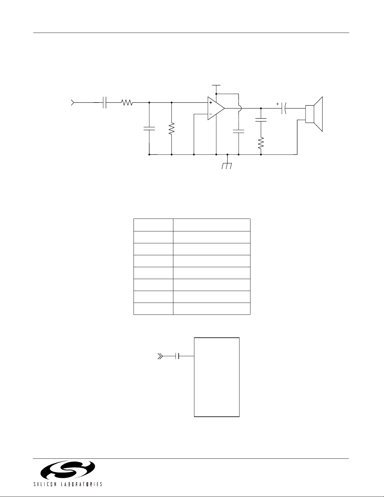
Figure 4 illustrates a n optional application circuit to support the analog output ca pability of the Si2400 for voi ce
monitoring purposes.
+5V
C2
AOUT
R3
C6
R1
6
3
2
5
U1
4
C3
C4
C5
Speaker
R2
Figure 4. Optional Connection to AOUT for a Monitoring Speaker
‘
Table 10. Component Va lues—Optional Connection to AOUT
Symbol Value
C2, C3, C5 0.1 µF, 16 V, ±20%
C4 100 µF, 16 V, Elec. ±20%
C6 820 pF, 16 V, ±20%
R1 10 kΩ, 1/10 W, ±5%
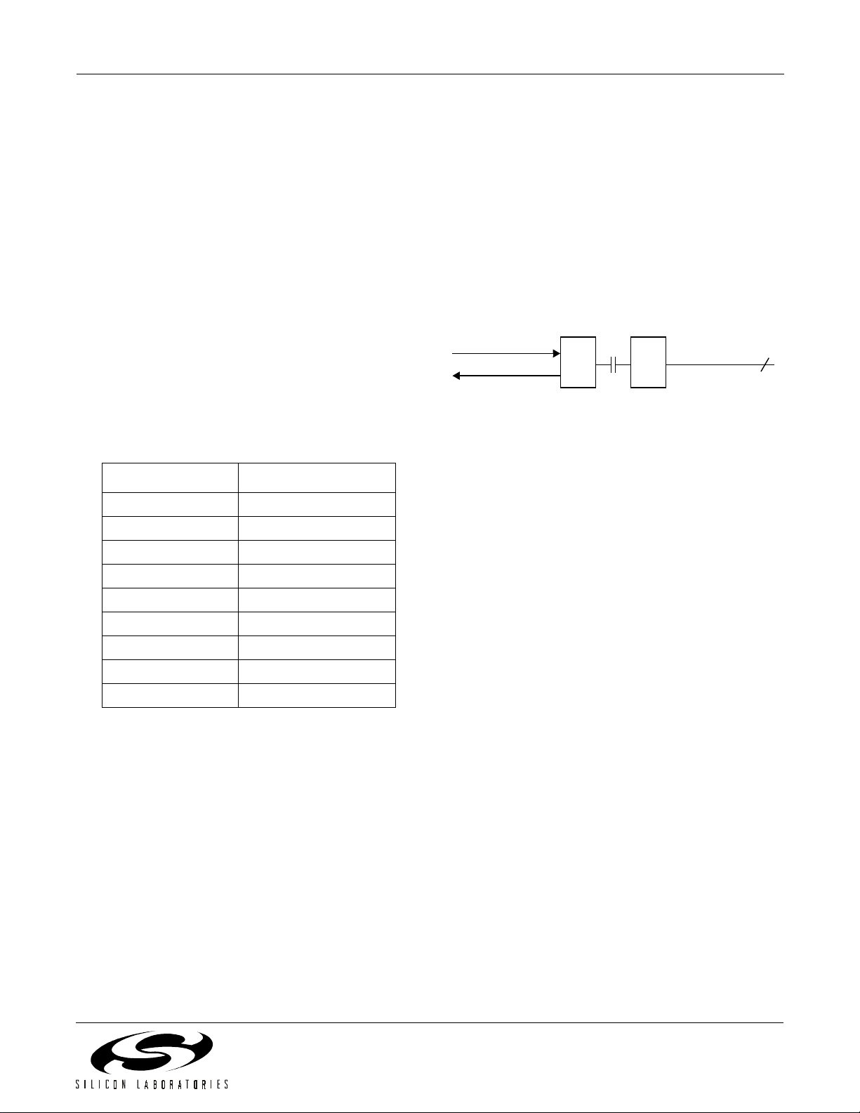
Analog Input
Figure 5. Analog Input Circuit
R2 10 Ω, 1/10 W, ±5%
R3 47 kΩ, 1/10 W, ±5%
U1 LM386
Si2400
AIN/GPIO
0.1 µF
1 Vrms
Rev. 0.95 11
Page 12

Si2400
Functional Description
The Si2400 ISOmodem is a complete modem chipset
with integrated direct access arrangement (DAA) that
provides a programmable line interface to meet global
telephone line requirements. Available in two 16-pin
small outline pa cka ge s, this sol ut io n inc lud es a D SP dat a
pump, a modem co ntroller, an analog fron t end (AFE), a
DAA, and an audio co de c.
The modem, which accepts simple modem AT
commands, provides connect rates of up to 2400 bps,
full-duplex over the Public Switched Telephone Network
(PSTN) with V.42 hardware support through HDLC
framing. To minimize handshake times, the Si2 400 can
implement a V.25-based fast connect feature. The
modem also su pp or ts the V.23 reversing pr oto col a s we ll
as SIA and other al ar m sta nd ard fo rma t s.
As well as suppor ting the modem si gnallin g proto cols, th e
ISOmodem provides numerous additional features for
embedded mode m ap pl ic a ti on s. T he S i 24 00 in c lu de s full
caller ID detection and decoding for the US, UK, and
Japanese caller ID formats. Both DTMF decoding and
generation are prov ided on chip a s well. Call pro gres s is
supported both at a high level through echoing result
codes and at a low level through user-programmable
biquad filters and parameters such as ring period, ring
on/off time, and dialing interdigit time.
This device is ideal for embedded modem applications
due to its small board space, low power consumption,
and global compliance. The Si2400 solution integrates a
silicon DAA using Silicon Laboratories’ proprietary
ISOcap™ technology. This highly integrated DAA can be
programmed to meet worldwide PTT specifications for
AC termination, DC termination, ringer impedance, and
ringer thresh old. The DAA a lso can mon itor l ine st atu s for
parallel handset detection and for overcurrent conditions.
The Si2400 is designed so that it may be rapidly
assimilated into existing modem applications. The device
interfaces directly through a UART to either a
microcontroller or a standard RS-232 connection. This
simple interfa ce allows for PC evalua tion of the modem
immediately up on po we rup v i a t he AT commands across
a standard hyperterminal.
The chipset can be fully programmed to meet
international telephone line interface requirements with
full compliance to FCC, CTR21 , JATE, and other countryspecific PTT specifications. In addition, the Si2400 has
been designed to meet the most stringent worldwide
requirements for out-of-band energy, billing-tone
immunity, lightning surges, and safe ty re qu ire me nts .
The Si2400 solut ion needs only a few low-cost disc rete
components to achieve global compliance. See Figure 3
on page 9 for a typi cal ap pli cati on cir cu it .
Table 11. Selectable Configurations
Configuration Modulation
V.21 FSK 1080/1750 300 Full
V.22 DPSK 1200/2400 1200 Full
V.22bis (1200 fallback) DPSK 1200/2400 1200 Full
V.22bis QAM 1200/2400 2400 No retrain*
V.23
FSK
V.23 1300/1700 600/75
Bell 103 FSK 1170/2125 300 Full
Bell 212A DPSK 1200/2400 1200 Full
Security DTMF — 40 Full
SIA—Pulse Pulse — Low Full
SIA Format FSK 1 170/2125 300 half-duplex 300 bps only
*Note: The Si2400 only adjusts its baud ra te for li ne condi tions during the in itiali zation of the ca ll. Retra ining to a ccommo date
changes in line conditions which occur during a call must be implemented by terminating the call and redialing.
Carrier
Frequency (Hz)
1300/2100 1200/75
Data Rate
(bps)
Standard
Compliance
Full; plus reversing
(Europe)
12 Rev. 0.95
Page 13
Si2400
Digital Interface
The Si2400 has an asynchronous serial port (UART)
that supports st andard microcontroller interfaces. After
reset, the baud rate defaults to 2400 bps with the 8-bit
data format described bel ow. Immediately after powerup, the device must be progr ammed using the primary
serial port because the secondary serial port is disabled
by default. The CLKOUT clock will be running with a
frequency of 9.8304 MHz.
The baud rate of the serial l ink is e stablished by writin g
S register SD (SE0.2:0). It may be set for 300, 1200,
2400, 9600, 19200, 228613, 245760, or 307200 bps.
Immediately after the ATSE0=xx string is sent, the user
must reprogram the host UART to matc h the selected
new baud rate. The higher baud rate settings (>230400)
can be used for tra nsferring PCM d ata from the host to
the Si2400 for transmission of voice data over the
phone line or through the voice codec.
Table 12. Register S07 Examples: DTMF = 0,
HDEN = 0, BD = 0
Modem Protocol Register S07 Values
data bits, and the line data fo rmat is 8 data bits (8N1),
then the MSB from the l ink will be dropped as the 9-bit
word is passed from the link sid e to the line si de. In this
case, the dropped ninth bit can then be used as an
escape mechanism. However, if the link data format is 8
data bits and the line data fo rm at i s 9 data b its , an MSB
equal to 0 will be added to the 8- bit wor d as it is pas se d
from the link side to the line side.
The Si2400 UART does not continuou sly c heck for sto p
bits on the incom ing digital data. Ther efore, if the RXD
pin is not high, the TXD pin may transmit mean ingless
characters to the host UART. This requires the host
UART to flush its receiver FIFO upon initialization.
RXD UART
TXD
Link Line
Data Rate: SD (SE0.2:0)
Data Format: ND (SE0.3)
Si2400 Si3015
RJ11
Data Rate: S07
Data Format: S15
Figure 6. Link and Line Data Formats
V.21 0x03
Bell 103 0x01
V.22 0x02
Bell 212A 0x00
V.22bis 0x06
V.23 (75 tx, 1200 rx) 0x24
V.23 (1200 tx, 75 rx) 0x14
V.23 (75 tx, 600 rx) 0x20
V.23 (600 tx, 75 rx) 0x 10
Configurations and Data Rates
The Si2400 can be configured to any of the Bell and
CCITT operation modes. This device also suppo rts SIA
and other security modes for the security industry.
Table 11 provides the modulation method, the carrier
frequencies, the data rate, the baud rate and the notes
on standard complianc e for each modem configuratio n
of the Si2400. Table 12 shows example register settings
(SO7) for some of the modem configurations.
As shown in Figure 6, 8-bit a nd 9-bit data modes refer
to the link data format over the UART. Line data formats
are configured through registers S07 and S15. If the
number of bits specified by the link data format differs
from the number of bits specified by the line data
format, the MSBs will either be dropped or bit-stuffed,
as appropriate. For ex ample, if th e link data forma t is 9
Command/Data Mode
Upon reset, the modem will be in command mode and
will accept AT-style commands. An outgoing modem
call can be made using the “ATDT#” (tone dial) or
“ATDP#” (pulse dial) command after the device is
configured. If the handshake is successful, the modem
will respond with the “c”, “ d”, o r “v ” str i ng an d en ter data
mode. (The byte following the “ c”, “d”, or “v” will be the
first data byte.) At this point, A T-style commands are not
accepted. There a re thre e meth ods whic h may be u sed
to return the Si2400 to command mode:
!
Use the ESC pin—To program the GPIO3 pin to
function as an ESCAPE input, set GPIO3
(SE2.5:4) = 3. In this setting, a positive edge
detected on this pin will return the modem to
command mode. The “AT O” string can be used to reenter data mode.
!
Use 9-bit data mode—If 9-bit data format with
escape is programmed, a 1 detected on bit 9 will
return the modem to command mode. (See Figure 2
on page 8.) This is enabled by setting ND (SE0.3) =
1 and NBE (S15.0) = 1. The “ATO” string can be
used to reenter data mode.
!
Use TIES—The time independent escape sequence
is a sequence of three escape characters ("+"
characters by default). Once these characters have
been recognized, the modem enters the Command
state without sending a confirming result code to the
terminal. The modem then starts an internal prompt
Rev. 0.95 13
Page 14

Si2400
delay timer. From that point on if an AT<CR>
(attention) command is received before the timer
expires, the timer is stopped and the “O” response
code is sent to the terminal. This indicates that the
Si2400 is in command mode.
If any other data is received while the timer is
running, the timer is stopped, the device returns to
the online state, and the data received through the
UART RXD is sent to the other modem.
If the timer expires, a confirming “O” response code
is sent to the terminal indicating that the modem is in
command mode.
TIES can be enabled by writing register TED
(S14.5)=1. Both the escape character “+” and the
escape time-out period are programmable via
registers TEC (S0F) and TDT (S10), respectively.
Note: TIES is not the recommended escape solution for the
most robust designs. Any data strings that actually
contain the escape character three times in a row will
interrupt a data sequence erroneously.
Whether using an escape method or not, when the
carrier is lost, the modem will automatically return to
command mode and report “N”.
8-Bit Data Mode
This mode is asynchronous, full-duplex, and uses a
total of 10 bits (shown in Figure 2 on page 8). To
program 8-Bit Data mode, set ND (SE0.3) = 0. (Note
that 8-Bit Data mode is the defa ult.) The 10 bi ts consist
of a start bit (logic 0), 8 data bits, and 1 stop bit (logic 1).
Data transmission from the Si2400 to the host takes
place on the TXD pin. It beg ins whe n th e Si 24 00 l owers
TXD, placing the start bit on the pin. Data is then shifted
out onto the pin, LSB fi rst. After 8 data bits, th e stop bit
follows. All bits are s hi fted out a t the ra te d etermi ne d by
the baud rate register.
Once the baud rate register SD (SE0.2:0) is written,
reception by the Si2400 may begin at any time. The
falling edge of a start bit will signal to the Si2400 that the
reception process has begun. Data should be shifted
onto RXD at the selected baud rate.
After the middle of the stop-bit time, the receiver will go
back to looking for a 1 to 0 transition on the RXD pin.
9-Bit Data Mode
This mode uses a total of 11 bits in UART
communication. To program 9-Bit Data mode, set ND
(SE0.3) = 1. The 11 bits consist of one start bit (logic 0),
9 data bits, and 1 stop bit (logic 1, see Figure 2 on page
8). As in 8-Bit Data mode, the trans missions occur on
the TXD signal pin and receptions on the RXD pin.
Data transmission from the Si2400 to the host takes
place on the TXD pin. It beg ins whe n th e Si 24 00 l owers
TXD, placing the start bit on the pin. Data is then shifted
out onto the pin, LSB fi rst. After 9 data bits, t he stop bit
follows. All bits are shifted out a t the rate d eterm ine d by
the baud rate register.
Once the baud rate register SD (SE0.2:0) is written,
reception may begin at any tim e. The falling edge of a
start bit on the RXD pin will begin the reception process.
Data must be shifted in at the selected baud rate.
The ninth data bit may be used to indicate an escape by
setting NBE (S15.0) = 1. If so, this bi t will normally be
set to 0 when the modem is online. To go offline into
command mode, se t th is b it to 1. The next fram e wi ll b e
interpreted as a command. Data mode can be
reentered using the ATO command.
After the middle of the stop-bi t time, the rece iver will go
back to looking for a 1 to 0 transition on the RXD pin.
Flow Control
If a higher serial link line (UART) data rate is
programmed than the baud rate of the modem, flow
control is required to prevent loss of data to the
transmitter. No flow control is nee ded if the same baud
rate as modem rate is programmed. Note that in
compliance with the V.22bis algorithm, the V.22bis
(2400 baud) modem will connect at 1200 baud if it
cannot make a 2400 baud connection.
To control flow, the CTS
Figure 2 on page 8, the CTS
pin is used. As shown in
pin will normal ly be high,
and will be lo w whenever the m odem is able t o accept
new data. The CTS
pin will go high again a s soon as a
start bit is detected on the RXD pin and will remain high
until the modem is ready to accept another character.
Low Power Modes
The Si2400 has three low power modes. These are
described below:
!
DSP Powerdown. The DSP processor can be
powered down by setting register PDDE (SEB.3) =1.
In this mode the serial interface still functions as
normal, and the modem will be able to detect ringing
and intrusion. No modem modes or tone detection
features will function.
!
Wake Up On Ring. By issuing the “z” command, the
Si2400 goes into a low power mode where both the
microcontroller and DSP are powered down. Only
incoming ringing or a total reset will power up the
chip again.
!
Total Powerdown. By writing registers PDN (SF1.6)
and PDL (SF1.5), the Si2400 will be put into a total
powerdown mode. In this mode, all logic is powered
down, including the crystal oscillator and clock-out
pin. Only a hardware reset can restart the Si2400.
14 Rev. 0.95
Page 15

Si2400
Global DAA Operation
The Si2400 chipset co ntains an in tegrated sil icon direc t
access arrangement (silicon DAA) that provides a
programmable line interface to meet international
telephone line interface requirements. Table 13 gives
the DAA register setti ngs required t o meet internati onal
PTT standards. A detailed description of the r egisters in
Table 13 can be found in "Appendix A—DAA
Operation‚" on page 62.
Table 13. Country-Specific Register Settings
Register SF5 SF7 SF6
Country OHS ACT DCT RZ RT LIM VOL FNM
Australia 112 0000 0
Bulgaria 01200000
CTR21
Czech Republic 0 1 2 0 0 0 0 0
FCC 002 0000 0
Hungary 002 0000 0
Japan 001 0000 0
Malaysia
New Zealand 0 1 2 0 0 0 0 0
Philippines 001 00001
Poland
Singapore
Slovakia 01200000
Slovenia 01200000
South Africa
South Korea
1
2
3
2
3
3
013 0010 0
001 0000 0
002 1100 0
001 0000 0
112 1000 0
001 1000 0
Note:
1. CTR21 includes the following countries: Austria, Belgium, Cyprus, Denmark, Finland, France,
Germany, Greece, Iceland, Ireland, Israel, Italy, Liechtenstein, Luxembourg, Netherlands, Norway,
Portugal, Spain, Sweden, Switzerland, and the United Kingdom.
2. Supported for loop current ≥ 20mA.
3. The RZ register (SF5.1) should only be set for Poland, South Africa and South Korea if the ringer
impedance network (C15, R14, Z2, Z3) is not populated.
Parallel Phone Detection
The Si2400 has the abilit y to detect another phone that
is off hook on a shared li ne. This all ows the ISO modem
both the ability to avoid interrupting another call on a
shared line and to intelligently handle an interruption
when the Si2400 is using the line. An automatic
algorithm to detect paralle l phone intrusion (defined as
an off-hook parallel handset) is provided by default.
On-Hook Intrusion Detection
The on-hook intrusion detection allows the user to avoid
interrupting another ca ll on a shared line. To implement
the intrusion detecti on, the Si2400 uses a loop vol tage
sense (register LVCS (SDB)). When on hook, LVCS
monitors the line voltage. ( When off hook, it measures
current.) LVCS has a full scale of 70 V with an LSB of
2.25 V. The first code (0 → 1) is skewed such that a 0
indicates that the line voltage is < 3.0 V. The voltage
accuracy of LVCS is ±20%. The user can read these
bits directly when on hook through register LVCS.
The automatic on-hook detector algorithm can be
tripped by either an absolute level or by a voltage
differential by selecting ONHD (S13.3). If the absolut e
detector is chosen, th e Si2400 algorithm will d etect an
intrusion if LVCS is less than the on-hook intrusion
Rev. 0.95 15
Page 16

Si2400
threshold, register AVL (S11.4:0). In other words, it is
determined that an intrusion has occurred if LVCS <
AVL.
AVL defaults to 0x0D, or 30 V on powerup. The
absolute detector is the co rrect method to use for FCC
and most other countries. T he absolu te detector sho uld
also be used to de tect the presence (or abs ence) of a
line connection.
Under the condition of a ver y short line and a currentlimiting telephone off hook, the off-hook line vo ltage can
be as high as 40 V. The minimum on-hook voltage may
not be much greater. This condition can occur on phone
30
25
20
LVCS
BIT
15
lines with current-li mi tin g s pec if ic ations s uch as Fra nce.
For these lines, a differential detector is more
appropriate.
The differential detector method checks the status of the
line every 26.66 ms. The detec tor compares (LVCS (t –
0.02666) – LVCS (t)) to the differential threshold level
set in register DVL (S11.7:5). The default for DVL is
0x02 (5.25 V). If the threshold is ex ceeded (LVCS (t –
0.02666) – LVCS (t) > D VL), an in trusion is detected. If
(LVCS (t) – LVCS (t – 0.02666) > DVL), then the
intrusion is said to have terminated.
10
5
0
0
36 33302724211815129 3639424548
Loop Voltage
Figure 7. Loop Voltage—LVCS T ransfer Function
Off-Hook Intrusion Detection
When the Si2400 is off hook, it can detect another
phone going off hook by monitoring the DC loop current.
The loop current sense transfer function is shown in
Figure 8 with the upper curve representing CTR21
(current limiting) operation and the lower curve
representing all other modes. The overload points
indicate excessive current draw. The user can read
these bits directly through register LVCS (SDB). Note
that as in the line voltage sense, there is hysteresis
between codes (0.375 mA for CTR21 mode and
0.75 mA for ROW).
7269666360575451
100
16 Rev. 0.95
Page 17
Si2400
Overload
30
25
LCS
BIT
20
15
10
5
0
0
36 33302724211815129 3639424548
CTR21
Loop Current (mA)
Figure 8. Loop Current—LVCS Transfer Function
The off-hook algorithm can be chosen to use eithe r a
differential current detector or an absolute current
detector via setting OFHD (S13.4).
Because of the extra code and host processing required
by the absolute current method, the differe ntial current
method is chosen to be the defau lt. This method uses
two techniques to detect an intrusion. The first
technique is described as follows:
If (LVCS (t – 400 ms) – LVCS (t)) > DCL, then an
intrusion is deem ed to have taken place. If (LVCS (t) –
L VCS (t – 400 ms)) > DCL, then the intrusion is deemed
to have completed. Default DCL is 2.
The second technique takes advantage of the DC
holding circuit. If a parallel phone suddenly goes off
hook, the DC holding circuit will not reac t immediately,
therefore the loop c urrent through the Si2400 will drop
briefly to zero. Thus, an i ntrusion is als o reported when
LVCS = 0.
If the absolute detector is chosen, the Si2400 will detect
an intrusion under the condi tion that LVCS is less than
the off-hook intrusion threshol d, regi ster A CL (S12.4: 0).
In other words, it is determined that an intrusion has
occurred if LVCS < ACL. ACL defaults to 3 (15.5 mA) on
powerup. Because the loop current can vary from
20 mA to 100 mA, depending on the line, a factory
preset threshold is not useful.
If the host wishes to use this absolute mode, the host
must measure the line current and then set the
threshold accordingly. A measurement of the loop
7269666360575451 75 78 81 84 87 90 93
140
current is accomplished by going off-hook (issuing the
“ATDT;” command), reading LVCS after 50 ms, and
going back on hook using the “ATH” command. This
measured value of LVCS should be used to determine
the threshold register ACL. If this method is used, the
loop current should b e measur ed on a pe riodic bas is to
account for drift in line resistance.
The absolute curren t method is the most accu rate, and
it is necessary to use thi s method in order to determ ine
if another phone goes off hook simultaneous with or
immediately (< 400 ms) af ter the Si 240 0 phon e goe s off
hook. It does, however, require processi ng by the host,
including periodic off-hook events to measure the loop
current.
If an intrusion event is detected while in command
mode, an “i” is echoed to the host; When it is terminated
an “I” is echoed. The host may also be notified of an
intrusion when in data mo de through the A LERT pin by
setting GPIO4 (SE2.7:6) = 3. Upon intrusion, the
ALERT pin will go high, and the host may then read
register IND (S14.1) to confirm an intrusion.
The host may use the automatic intrusion detection
algorithm (the default ) by monitoring the ALERT pin or
waiting for the character echoes. The host may also use
the LVCS, AVL, and DVL registers as a basis for a
custom algorithm. Note that LVCS only acts as a line
voltage sense when on hook. When off hook, it
becomes the line current sense register.
Rev. 0.95 17
Page 18

Si2400
Carrier Detect/Loss
The Si2400 can provide the functionality of a loss-ofcarrier pin similar t o the CD pin functionality in an R S232 connection. If programmed as an ALERT, GPIO4
will go high in online mod e when either parallel phone
intrusion or a loss-of- carrier is detected. When used in
this manner, the host detects a low-to-high trans ition on
GPIO4 (ALERT), escapes into command mode, and
reads register IND (S14.1). If high, IND indicates
intrusion. If low, IND indicates loss-of-carrier.
Overcurrent Protection
The Si2400 has built in prote ction to avoid damage to
the device due to overcurrent situations. An example
situation occurs when plugging the m ode m i nto a d igital
PBX outlet and attempting to go off-hook. Digital PBX
systems vary, but many can provide a DC feed vol tage
of up to 70 V and therefore have the ability to deliver
hundreds of milliamps of current into the DAA.
The Si2400 will always go off hook with the currentlimiting mode enabled. This allows no possibility of
damage for voltages up to about 48 V. However, at
higher voltages the 43 V Zener protection device will
begin to conduct and co uld be damaged if the power is
applied for too long.
The Si2400 will det ect the v alue of the lo op cur rent at a
programmable time after going off-hook (default =
20 ms) via register OHT (S32). If the loop current is too
high, an “x” will be echoed back to the host to indi ca te a
fault condition. The host may then check register OD
(S14.3) to confirm an overcurrent condition and go back
on hook if necessary.
The user can optionally enable another protection
feature, the overcurrent protection, via register AOC
(S14.4). This protection feature can automatically detect
an overcurrent condition and put the Si2400 into a lower
drive mode, which is si milar to the current-limi ting mod e
but has reduced hoo kswitch drive. This feature allows
the Si2400 to remain off-hook on a digital line for a
longer period of time without damage. If the Si2400
does not detect over current aft er the time s et by OCDT
(S32), then the c orrect line terminat ion is applied. This
method of going off hook in current-limiting mode can
be disabled by clearing OFHE (S13.5).
Caller ID Decoding Operation
The Si2400 supports ful l cal le r ID d etecti on a nd dec od e
for US Bellco re, UK, and Japanese standards. To use
the caller ID decoding feature, the following set-up is
necessary:
1. Set ND (SEO.3) = 0 (Set modem to 8N1 configuration)
2. Set CIDU (S13.1) = 1(Set modem to Bellcore type caller
ID) or CIDB (S13.2) = 1 (Set modem to UK type caller ID)
or JID (S13.7) = 1 (Set modem to Japanese type caller ID)
3. Set baud rate either to 1200 bps without flow control or
greater than 1200 bps with flow control.
Bellcore Caller ID Operation
The Si2400 will d etect the fir st ring burst sig nal and will
echo an “R” to the host. The device will then start
searching for the call er ID preamb le sequen ce after the
appropriate time-out. When 50 continuous mark bits
have been detected, the “m” res pon se will be ec hoe d to
indicate that the mark has been detected and that caller
ID data will follow.
At this point the algorith m will look for the first start bi t,
assemble the characters, and then transmit them out of
the UART as they are detected. When the caller ID
burst finishes, the carrier will be lost and the modem will
echo an “N” to indicate that the carrier is lost.
At this point the Si2400 will continue detecting ring
bursts and echoing “R” for each burst, and will
automatically answer after the correct number of rings.
UK Caller ID Operation
When the Si2400 detect s a line reversa l, it will echo an
“f” to the host. It will then start searching for the Idle
State Tone Alert Signal. When this signal has been
detected, the Si2400 will transmit an “a” to the host.
After the Idle State Tone Alert Signal is completed, the
Si2400 will apply the wetting pulse for the required
15 ms by quickly going o ff hook and o n hook . From th is
point on, the algorithm is identical to that of B ellcore in
that it will search f or the chan nel seizu re signal and the
marks before echoing an “m” and will then report the
decoded caller ID data.
Japan Caller ID Operation
After a polarity reversal and the first ring burst are
detected, the Si2400 is taken off hook. After 40 1s
(marks) have been det ected, the Si24 00 will search for
a start bit, echo an “m” for mar k, and begin asse mbling
characters and tra nsmitting them out through the s erial
port. When the carrier is lost, the Si2400 immediately
hangs up and echoes “N” . Al so, if no ca rrie r is d etecte d
for three seconds, the line hangs up and echoes “N”.
Force Caller ID Monitor
The Si2400 may be used to continuously monitor the
phone line for the caller ID mark signal s. This can be
useful in systems that require dete cti on of calle r ID data
before the ring sign al, voice mail indic ator signals, and
Type II caller ID support. To force the Si2400 into caller
ID monitor mode, set CIDM (S0C.5).
18 Rev. 0.95
Page 19
Si2400
Tone Generation and Tone Detection
The Si2400 provides comprehensive and flexible tone
generation and detection. This includes all tones
needed to establish a circuit connection and to se t up
and control a communication session. The tone
generation furnishes the DTMF tones for PSTN auto
dialing and the supervisory tone s for cal l establi shmen t.
The tone detection provides support for call progress
monitoring. The detect or can a lso be user- programme d
to recognize up to 16 DTMF tones and two tone
detection bandpass filters.
DTMF tones may be dete cted and generated by using
the “ATA0” and “AT!0” c ommands described in the AT
command section. A description of the userprogrammable tones can be found in "Modem Result
Codes and Call Progress‚" on page 30.
PCM Data Mode
The Si2400 has the ability to bypass the modem
algorithm and send 14-bit PCM data, sampled at
9600 Hz, across the DAA. To use this mode, it is
necessary to set the serial link baud rate to at least
228613 bps (SE0), set PCM (S13.0) = 1, and set MCKR
(E1.7:6) = 0. The data format (Figure 9) requires that
the high byte be sent first contain ing bits D13–D7. The
LSB (B0) must e qual zero. The low by te must be sent
next containing bits D6–D0; the LSB (B0) must equal
one. The receive data format is the same.
In PCM data mode, the line can be answ ered using th e
“ATA;” command or a call can be origina ted using the
“A TDT#;” command. (The “;” is used to keep the modem
from leaving the command mode.) When PCM data
mode is enabled (set PCM (S13.0) = 1 and DRT
(SE4.5:4) = 0 (default)), data will immediately begin
streaming into and out of the serial port at a 9600 H z*2
word rate. In this mode, the controller will not detect dial
tones or other ca ll progress tones. If desi red, the user
can monitor these tones using manual call progress
detection prior to entering the PCM data mode.
To exit the PCM data mode, an escape must be
performed either by p ulsing the ES C pin or by using 9bit data mode and setting th e ninth bit. (TIES c annot b e
used in PCM data mode.) The escape command will
disable PCM streaming, and the controller will again
accept AT style commands.
Note: PCM data mode is the format that must also be used
when the Si2400 is configured to run as a voice codec
(DRT = 3).
PCM Receive Timing
8-Bit Data
TXD
Start
D7 D8 D9 D10 D11 D12 D13 D0 D1 D2 D3 D4 D5 D6
B0
B1
B2 B3 B4 B5 B6 B7
High-Byte
Stop
Start
Low-Byte
B0
B1 B2 B3 B4 B5 B6 B7
PCM Transmit Timing
8-Bit Data
RXD
Start B1
Note: Baud rates (programmed through register SE0) can be set to the following: 228613, 245760, and 307200.
D7 D8 D9 D10 D11 D12 D13 D0 D1 D2 D3 D4 D5 D6
B0
High-Byte
B2 B3 B4 B5 B6 B7
Stop
Start
Low-Byte
B0
B1 B2 B3 B4 B5 B6 B7
Figure 9. PCM Timing
Stop
Stop
Rev. 0.95 19
Page 20
Si2400
A.
TX
RX
RXD
TXD
DSP
DSPOUT
DSPIN
Data Mode (DRT = 0)
Si2400
Si3015
RJ11
RJ11
B.
C.
TX
RX
TX
RX
RXD
TXD
RXD
TXD
DSP
DSPOUT
DSPIN
DSP
DSPOUT
DSPIN
AOUT
(Call Progress)
Voice Mode (DRT = 1)
Si2400
AIN
AOUT
(Voice Out)
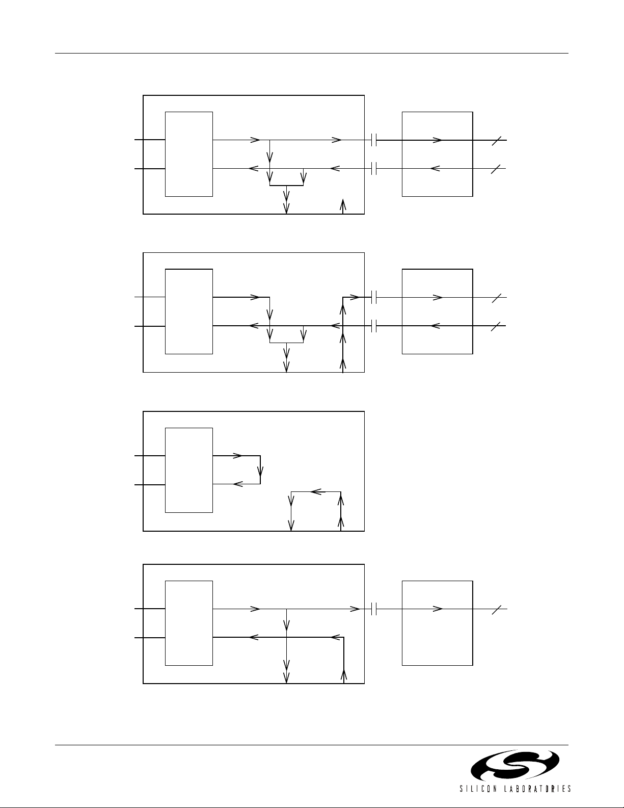
(Voice In)
Loopback Mode (DRT = 2)
Si2400
AIN
Si3015
RJ11
RJ11
AIN
AOUT
Codec Mode (DRT = 3)
Si2400
DSP
RXD
TX
D.
20 Rev. 0.95
RX
TXD
DSPOUT
DSPIN
AIN
AOUT
(Voice Out)
Figure 10. Signal Routing
AIN
Si3015
RJ11
AIN
(Voice In)
Page 21

Si2400
Analog Codec
The Si2400 features an on-chip, voice quality codec.
The codec consists of a digital to analog converter
(DAC) and an analog to digital converter (ADC). The
sample rate for the codec is set to 9.6 kHz. Wh en the
codec is powered on (s et register APO (SE 4.1)=1), the
output of the DAC is always present on the Si2400
AOUT pin. When the c ode c is po wer ed off (APO = 0), a
PWM output is present on the AOUT pin instead. In
order to use the ADC , one of the four GPIO pins must
be selected as an analog input ( AIN) by programming
the GPIO register (SE2).
Figure 10 shows the various signal routing modes for
the Si2400 voice codec, which are programmed through
register DRT (SE4.5:4). Figure 10A shows the data
routing for data mode. This is the default mode, which is
used for the modem data forma ts. In this configurat ion,
AOUT produces a mixed sum of the DSPOUT and
DSPIN signals and is typically used for call progress
monitoring through an external speaker. The relative
levels of the DSPOUT and DSPIN signals that are
output on the AOUT pin can be set through registers
ATL (SF4.1:0) and ARL (SF4.3:2).
Figure 10B shows the format for sending analog v oice
across the DAA to the PSTN. AIN is routed directly
across the DAA to the telephone line. In this
configuration, AOUT produces a mixed sum of the
DSPOUT and DSPIN signals . The relative levels of the
DSPOUT and DSPIN signals that are output on the
AOUT pin can be set through registers ATL (SF4.1:0)
and ARL (SF4.3:2). Note that the DSP may process
these signals if i t is not in PCM data mode. Thus, th e
DSP may be used in this configuration, for exam ple, to
decode DTMF tones. This is the mode used with the “!0”
and “A0” commands.
Figure 10C shows the loopback format, which can be
used for in-circuit t esting. A detailed description of the
in-circuit test modes is des cribed in the "Appendix A—
DAA Operation‚" on page 62.
Figure 10D shows the codec mode. This format is
useful, for example, in voice prompting, speaker
phones, or any systems involving digital signal
processing. In this mode, DSPOUT is routed to both the
AOUT pin and to the telephone li ne, and AIN is routed
directly to DSPIN.
Note that in all the DRT formats, the DSP must be in
PCM mode in order to pass DSPIN and DSPOUT
directly to and from TXD and RXD.
V.23 Operation/V.23 Reversing
The Si2400 supports full V.23 operation including the
V.23 reversing procedure. V.23 operation is enabled by
setting MF8 (S07) = xx10xx00 or xx01xx00. If V23R
(S07.5) = 1, then the Si2400 will transmit data at 75 bps
and receive data at either 600 or 1200 bps. If V23T
(S07.4) = 1, then the S i2400 will receive da ta at 75 bps
and transmit data at either 600 or 1200 bps. BAUD
(S07.2) is the 1200 or 600 bps ind icator. BAUD = 1 will
enable the 1200/600 V.23 channel to run at 1200 bps
while BAUD = 0 will enable 600 bps operation.
When a V.23 connection is successfully established, the
modem will respond with a “c” character if the
connection is made with the modem transmitting at
1200/600 bps and receivi ng at 75 bps. The m odem will
respond with a “v” character if a V.23 connection is
established with the modem transmitting at 75 bps and
receiving at 1200/600 bps.
The Si2400 supports a V.23 turnaround procedure. This
allows a modem th at is tran smitting at 75 bps to init iate
a “turnaround” procedure so that it can begin
transmitting data at 1200/600 bps an d receiv ing data a t
75 bps. The modem is define d as being in V.23 master
mode if it is transmi tting at 75 bps and it is defi ned as
being in slave mode if the modem is transmitting at
1200/600 bps. The f ollowi ng pa ra gr aph s gi ve a d etai le d
description of the V.23 turnaround procedure.
Modem in master mode
To perform a direct turnaround once a modem
connection is established, the host goes into onlinecommand-mode by sending an escape command
(Escape pin activation, TI ES, or ninth bit esc ape) to the
master modem. (Note that the host can initiate a
turnaround only if the Si2400 is the master.) The host
then sends the ATRO command to the Si2400 to initiate
a V.23 turnaround and to go bac k to the online (data)
mode.
The Si2400 will then change its carrier frequency (from
390 Hz to 1300 Hz), and wait for detecting a 390 Hz
carrier for 440 ms. If the modem detects more than
40 ms of a 390 Hz carrier into a time window of 440 ms,
it will echo the “c” response character. If the modem
does not detect more than 40 ms of a 390 Hz carrier
into a time window of 44 0 ms, it will hang up and ech o
the “N” (no carrier) character as a response
Modem in slave mode
The Si2400 performs a reverse turnaround when it
detects a carrier drop longer than 20 ms. The Si2400
then reverses (it changes its carrier from 1300 Hz to
390 Hz) and waits to detect a 1300 Hz carrier for
220 ms. If the Si2400 detects more than 40 ms of a
Rev. 0.95 21
Page 22

Si2400
1300 Hz carrier in a time window of 22 0 ms, then it will
set the ALERT pin (GPIO4 must be configured as
ALERT) and the next charac ter echoed by the Si2400
will be a “v”.
If the Si2400 does not detect more than 40 ms of the
1300 Hz carrier in a time window of 220 ms, then it
reverses again and waits to detect a 3 90 Hz carrier for
220 ms. Then, if the Si2400 detec ts mo re than 40 ms of
a 390 Hz carrier in a time window of 220 ms, it will set
the ALERT pin and the next character echoed by the
Si2400 will be a “c”.
At this point, if the Si2400 does not detect more than
40 ms of the 390 Hz carrier in a time window of 220 ms,
then it will hang up, set the ALERT pin, and the next
character echoed by the Si2400 will be an “N” (no
carrier).
Successful completion of a turnaround procedure in
either master or slave will automatically update V23T
(S07.4) and V23R (S07 .5) to indicate the new statu s of
the V.23 connection.
In order to avoid using the ALERT pin, the host may
also be notified of t he ALERT condition by using 9-bit
data mode. Setting NB E (S15.0) = 1 a nd 9BF (C .3) = 0
will configure the ninth bit on the Si2400 TXD path to
function exactly as the ALERT pin has been described.
V.42 HDLC Mode
The Si2400 supports V.42 through HDLC framing in
hardware in all modem data modes. Frame packing and
unpacking, including opening and closing flag
generation and detection, CRC computation and
checking, zero inse rtion and deletio n, and modem data
transmission and reception are all performed by the
Si2400. V.42 error correction and data compression
must be performed by the host.
The digital link interface in this mode uses the same
UART interface (8-Bit Data and 9-Bit Data formats) as in
the asynchronou s modes and the nin th data bit may b e
used as an escape b y setting NBE (S15.0) = 1. When
using HDLC in 9-Bit Data mode, if the ninth bit is not
used as an escape, it is ignored.
To use the HDLC feature on the Si2400, the hos t must
first enable HDLC operation by setting HDEN
(S07.7) = 1. Next, the host may initiate the call or
answer the call using either the “ATDT#”, the “ATA”
command, or the auto- answer mode . (The auto -answer
mode is implemented by se tting register NR (S0) to a
non-zero value.) When the call is connected, a “c”, “ d”,
or a “v” is echoed to the host controller. The host may
now send/receive data across the UART using either
the 8-Bit Data or 9-Bit Data formats with flow control.
At this point, the Si24 00 will begin framing da ta into the
HDLC format. On the transmit side, if no data is
available from the host, the HDLC flag pattern is sent
repeatedly. When data is available, the Si2400
computes the CRC code throughout the frame and the
data is sent with the HDLC zero-bit insertion algorithm.
HDLC flow control operates in a similar manner to
normal asynchronous flow control across the UART and
is shown in Figure 11. In order to operate flow control
(using the CTS
pin to indicate when the Si2400 is ready
to accept a character), a higher serial link baud rate
than the transmission line rate should be selec ted. The
method of transmitting HDLC frames is as follows:
1. After the call is connected, the host should begin sending
the frame data to the Si2400, using the CTS
ensure data synchronicity. A 1-deep character FIFO is
implemented in the Si2400 to ensure that data is alway s
available to transmit.
2. When the frame is complete, the host should simply stop
sending data to th e Si240 0. As sho wn i n Figure11B, since
the Si2400 does not yet recognize the end-of-frame, it will
expect an extra byte and assert CTS
cause a host interrupt, then this final interrupt should be
ignored by the host.
3. When the Si2400 is ready to send the next byte, if it has
not yet received any data from the host, it will recognize
this as an end-of-frame, raise CTS
code, transmit the code, and begin transmitting stop flags.
4. After transmitting the first stop flag, the Si2400 will lower
CTS indicating that it is ready to receive the next frame
from the host. At this point the process repeats as in
step 1.
, calculate the final CRC
flow control to
. If CTS is used to
The method of receiving HDLC frames is as follows:
1. After the call is connected, the Si2400 searches for flag
data. Then, once the first non-flag word is detected, the
CRC is continuously computed, and the data is sent
across the UART (8-Bit Data or 9-Bit Data mode) to the
host after removing the HDLC zer o-bi t in sertio n. The baud
rate of the host must be at least as high as that of data
transmission. HDLC mode only works with 8-bit data
words; the ninth bit is used only for escape on RXD and
EOFR on TXD.
2. When the Si2400 detects the stop flag, it will send the last
data word in the frame as well as the two CRC bytes and
determine if the CRC checksum matches or not. Thus, the
last two bytes are not frame data, but are the CRC bytes,
which can be discarded b y the host. If the checksum
matches, then the Si2400 echoes “G” (good). If the
checksum does not match, the Si2400 echoes “e” (error).
Additionally, if the Si2400 detects an abort (seven or more
contiguous ones), then it will echo an “A”.
When the “G”, “e”, or “A” (referred to as a frame result
word) is sent, the Si2400 raises the EOFR (end of frame
receive) pin (see Figure 10B). The GPIO1 pin must be
configured as EOFR by setting GPE (SE4.3) = 1. In
addition to using the EOFR pin to indicate that the by te is a
22 Rev. 0.95
Page 23

Si2400
frame result word, if in 9-bit data mode (se t NBE (S15.0) =
1), the ninth bit will be raised if the byte is a frame result
word. To program this mode, set 9BF (S0C.3) = 1 and ND
(SEO.3) = 1.
3. When the next frame of data is detec ted, EOFR is low ered
and the process repeats at step 1.
To summarize, the host will begin receiving data
asynchronously from the Si2400. When each byte is
received, the host sh ould check the EOFR pin (or the
ninth bit). If the pin (or the ninth bit) is low, then the data
is valid frame data. If the pin (or the ninth bit) is high,
then the data is a frame result word.
Fast Connect
In modem applications that require fast connection
times, it is possible to expedite the handshaking by
bypassing the answer tone. The No Answer Tone (NAT)
bit (S33.1) is intende d to provid e a method to decreas e
the time needed to complete modem handshaking. If
the NAT bit is set, the Si2400 will bypa ss transmi tting a
2100 Hz or 2225 Hz ans wer tone whe n recei ving a call .
Instead, the modem will immediately begin the
handshaking sequence that normally follows answer
tone transmission. For example, when the modem is
configured as a V.22 answering modem, activating the
NAT bit will cause the mod em to immediately transmit
unscrambled ones at 1200 bps after the modem
connects to the line. In addition, register UNL (S20) may
be used to set the length of time that the modem
transmits unscrambled ones. Setting UNL to a value
lower than the default may also shorten the answer
sequence.
When the modem is set up to originate a call, setting the
NAT bit causes the modem to bypass the normal
answer tone search . Instead, the modem will sen d the
transmit sequence t hat normally occurs after receiv ing
the answer tone within 20 ms of th e start of the answ er
tone. For example, when the m odem is config ured as a
V.22 originating modem, activating the NAT bit will
cause the modem to start transmi tting scrambled ones
at 1200 bps within 20 ms of the start of an answer tone.
When NAT=0, additional modem handshaking control
can be adjusted through registers TATL (S1E), ATTD
(S1F), UNL (S20), TSOD (S21), TSOL (S22), VDDL
(S23), VDDH (S24), SPTL (S25), VTSO (S26), VTSOL
(S27), VTSOH (S28), RSO (S2A), FCD (S2F), FCDH
(S30), RATL (S31), TASL (S34), and RSOL (S35).
These registers c an be esp ecially us eful if t he user has
control of both the originating and answer modems.
Clock Generation Subsystem
The Si2400 contai ns an on-chip cl ock generator. Using
a single master clock input, the Si2400 can genera te all
modem sample rates necessary to support V.22bis,
V.22/Bell212A, and V.21/Bell103 standards as well a s a
9.6 kHz rate for audio playback. Either a 4.9152 MHz
clock on XTALI or a 4.9152 MHz crystal ac ross XTALI
and XTALO form the master clock for the S i2400. This
clock source is sent to an internal phase-locked loop
(PLL) which generates all necessary internal system
clocks. The PLL has a settlin g time of ~1 ms. Data on
RXD should not be sent to the dev ice pri or to se ttling of
the PLL.
A CLKOUT pin exists whereby a 78.6 432 MHz /(N + 1)
clock is produced which may be used to clock a
microcontroller or other devices in the system. N may
be programmed via CLKD (SE1.4:0) to any value from 1
to 31, and N defaults to 7 on power-up. The clock may
be stopped by setting N = 0.
The MCKR (microc ontroller clock rate r egister SEI.7:6)
allows the user to co ntrol the m icrocontrol ler cloc k rate.
On powerup, the Si2400 UART baud rate is set to
2400 bps, given that the clock inp ut is 4.91 52 MH z. Th e
MCKR register conserves power via slower clocking of
the microcontroller for specific applications where
power conservation is required. Table 14 shows the
configurations for different values of MCKR.
Note that if MCKR = 0, then all of the serial interface link
rates will run at either half (MCKR = 1) or quarter
(MCKR = 2,3) speed.
Table 14. MCKR Configurations
MCKR Modes Working
0
(9.8304 MHz)
1
(4.9152 MHz)
2,3
(2.4576 MHz)
All modes
All modes except
PCM streaming
and V22bis
Command modes
only
Rev. 0.95 23
Page 24

Si2400
Host begins frame N Host finished sending frame N Host begins frame N + 1
RXD
Si2400 ready for byte 1 of frame N
CTS
Note: Figure n o t to scale
Start Frame N Stop Start Frame N + 1
Si2400 detects
(CTS used as normal flow control)
end of frame N
Si2400 ready for byte 1
of frame N + 1
A. Frame Transmit
TXD
EOFR
(or bit 9)
Start Receive Data Stop
Start CRC Byte 1 Stop Start CRC Byte 2 Stop Start
B. Frame Receive
Figure 11. HDLC Timing
Frame Result Word
Stop
24 Rev. 0.95
Page 25

AT Command Set
The Si2400 supports a s ubset of the AT command set
as it is intended to be used with a dedicated
microcontroller in stead of the complete set required for
general terminal entry applications.
Command lines are typed to the modem when the
modem is in the Idle or Command state. Synta x for the
AT commands is case-sensitive.
A command line is defined as a string of characters
starting with the “A ” and “T” c haracters a nd ending with
a special end-of-line character, <CR> (13 decimal).
Command lines may contain several commands, one
after another. If there are no characters between “AT”
and <CR>, the modem responds with “OK” after the
carriage return.
Si2400
Table 15. AT Command Set Summary
Command Function
A Answer Line Immediately with Modem
DT# Tone Dial Number
DP# Pulse Dial Number
E Local Echo On/Off
H Hangup/Go On Line
I Return Product Code + Chip Revision
M Speaker Control Options
Command Line Execution
The characters in a command line are executed one at
a time. Unexpected command characters will be
ignored, but unexpected data characters may be
interpreted incorrectly.
After the modem has executed a command line, the
result code corresponding to the last command
executed is returned to the terminal or host. The
commands which warrant a response (e.g., “ATSR?”) or
“ATI” must be the last in the string and followed by a
<CR>. All other comman ds may be concatenated on a
single line. To echo command line characters, set the
Si2400 to echo mode using the E1 command.
All numeric arguments, including S-register numbers,
are in hexidecimal format and two digits must always be
entered.
< CR > End Of Line Character
This character is typed to end a command line. The
value of the <CR> char acter is 13, the ASCII carriage
return character. When the <CR> character is entered,
the modem executes the commands in the command
line. Commands which do not require a response are
executed immediately and do not need a <CR>.
O Return Online
RO V.23 Reverse
S Read/Write S Registers
w## Write S-Register in Binary
r# Read S-Register in Binary
m# Monitor S-Register in Binary
Z Software Reset
z Wakeup on Ring
AT Command Set Description
AAnswer
The “A” command makes the modem go off hook and
respond to an incoming call. This command is to be
executed after the Si2400 has indicated that a ring has
occurred. (The Si240 0 will indicate an inc oming ring by
echoing an “R”.)
This command is aborted if any other character is
transmitted to the S i2400 before the an swer process is
completed.
Auto answer mode is entered by setting NR (S0) to a
nozero value. NR indicates the number of rings before
answering the line.
Upon answering, the modem communicates by
whatever protocol has been de termined v ia the m odem
control registers in S07.
If no transmit car rier signal is rece ived from the callin g
modem within the time specified in CDT (S39), the
modem hangs up and enters the idle state.
Rev. 0.95 25
Page 26

Si2400
DDial
DT# Tone Dial Number.
DP# Pulse Dial Number.
The D commands make the modem dial a telephone
call according t o the digits and dial modif iers in the d ial
string following the c ommands . A maximum o f 64 digits
is allowed. A DT co mmand performs tone d ia li ng, a nd a
DP command performs pulse dialing.
The “ATS07=40DT;” command can be used to go off
hook without dialing.
The dial string must contain only the digits “0–9”, “*”, “#”,
“A”, “B”, “C”, “D”, or the modifiers “;”, “/”, or “,”. Other
characters will be interpreted incorrectly. The modifier
“,” causes a two second delay in dialing. The modifier “/”
causes a 125 ms delay in dialing. The modifier “;”
returns the device to command mode after dialing and it
must be the last character.
If any character is receiv ed by the Si2400 between the
ATDT#<CR> (or ATDP#<CR>) command and when the
connection is m ade (“c” is echoe d), the extra ch aracter
is interpreted as an abort, and the Si2400 returns to
command mode, ready to accept AT commands.
If the modem does not have to dial (i.e., “ATDT<CR>” or
“ATDP<CR>” with no dial string), the Si2400 assumes
the call was manually established and attempts to make
a connection.
E Command Mode Echo
Te lls the Si2400 whether or no t to echo character s sent
from the terminal when the modem is accepting AT
commands.
EO
Does not echo characters sent from the terminal.
E1
Echo characters sent from the terminal.
H Hangup
Hang up and go into command mode (go offline).
I Chip Identification
This command causes the modem to echo the chip
revision for the Si2400 device.
M Speaker On/Off Options
These options are used to contr ol AOUT for use with a
call progress monitor speaker.
M0
Speaker always off.
M1
Speaker on until carrier established.
M2
Speaker always on.
M3
Speaker on after last digit dialed, off at carrier detect.
O Return to Online Mode
This command returns the modem to the online mode. It
is frequently used after an esc ape sequence to resume
communication with the remote modem.
RO Turn-Around
This command initiates a V.23 “direct turnaround”
sequence and returns online.
S S Register Control
SR=N
Write an S register. This command writes the value “N”
to the S-register specified by “R”. “R” is a hexidecimal
number, and “N” must also be a hexadecimal number
from 00–FF. This command does not wait for a carr iage
return <CR> before taking effect.
Note:
Two di gits m ust alw ays be entered for both “R” and “N ”.
SR?
Read an S register. This command causes the Si2400
to echo the value of the S-register sp ecifi ed by R in hex
format. R must be a hexidecimal number.
Note: Two digits must always be entered for R.
w## Write S Register in Binary
This command writes a register in binary format. The
first byte following the “w” is the address in binary
format and the second byte i s the da ta in binar y forma t.
This is a more rapid method to writ e registers than the
“SR=N” command and is recommended for use by a
host microcontroller.
r# Read S Register in Binary
This command reads a register in binary format. The
byte following the “r” is the address in binary format.
The modem will echo the contents of this register in
binary format. This is a more rapid method to read
registers than the “SR?” command and is
recommended for use by a host microcontroller.
Notes: When using this command, the modem result
codes should be disabled by setting MRCD (S14.7) = 1.
This ensures that the host will not confuse a result code
with data being read.
w## and r# are not required to be on separate lines (i.e.,
no <CR> between them). Also, the result of an r# is
returned immediatel y without waiting for a <CR> at th e
end of the AT command line.
Once a <CR> is encounter ed, “AT” is again required to
begin the next “AT” command.
26 Rev. 0.95
Page 27

Si2400
m# Monitor S Register in Binary
This command moni tors a re gist e r in bi nar y for ma t. T h e
byte following the “ m” is the address in binary forma t.
The Si2400 constantly transmits the contents of the
register at the set baud rate until a new byte is
transmitted to the devi ce. The new byte is ig nored and
viewed as a stop command. The modem result co des
should be disabled (as described above in r#) before
using this command.
Z Software Reset
The “Z” command cau ses a software reset to occ ur in
the device whereby all registers will return to their
default power up value. If other commands follow on the
same line, another AT is needed after the “Z” (e.g.,
ATZATS07=06<CR>).
z Wakeup on Ring
The Si2400 enters a low-po wer mode wher ein the DSP
and microcontroller are powered down. The serial
interface also sto ps functioning. In this m ode, only the
line-side chip (S i3015) and the ISOcap communi cation
link function. An incoming ring signal causes the Si2400
to power up and echo a “w”. Without a rin g signal, the
host must perform a hardware reset to power up the
Si2400.
Table 16. AT Command Set Extensions
for Alarm Industry
Command Function
A0 Answer and switch to DTMF monitor mode
A1 Answer and switch to “SIA Format”
!0 Dial and switch to DTMF monitor mode
!1 Dial and switch to DTMF security mode
!2 Dial and switch to “SIA Format”
!3 Dial and swi t ch to GDC—P1
!4 Dial and swi t ch to GDC—P2
!5 Dial and swi t ch to GDC—P3
!6 Dial and swi t ch to GDC—P4
X1 SIA half-duplex mode search
X2 SIA half-duplex return online as
transmitter
X3 SIA half-duplex return online as receiver
Extended AT Commands for th e Alarm Industry
In addition to the AT command set used to make a data
modem connection, the Si2400 also supports a
complete set of commands required for making calls
and connections in security industry systems. These
commands are summarized in Table 16.
A0
After answering, connect AIN analog signal to phone
line transmit signal and output the phone line receive
signal to the AOUT pin (See Figure 10B). Also, this
mode monitors for DTM F received digits and the user
defined frequencies. A digit is reported by echoing the
character received. Transmission of any data to the
Si2400 UART will cause the modem to go into
command mode.
Once in command mode, the modem may be
disconnected with the “ATH” command, or DTMF tones
may be generated by using the “ ATDT#” command. (In
this case, “ATDT#” does not initiate a new call becaus e
the Si2400 has not been hung up and is still online.)
Online mode can be resumed by issuing the “ATO”
command. (User-de fined freque ncies a re reporte d as X
and Y for user defined frequencies 1 and 2,
respectively. To enable user-defined frequencies, set
UDF (S14.6) = 1.) Setting the user-defined f requencies
requires DSP low-level control.
A1
Answer line and follow the "SIA Format" protocol for
Alarm System Communications at 300 bps (see !2).
!0
After dialing the n umber, go into DTMF monitor mode
(no modem connection). After dialing is complete, the
connection is exactly the same as for the “AO”
command.
Note: When using “!” commands, the first instance of “!” must
be on the same line as the “ATDT#” or “ATDP#”.
!1
Dial number and follow the DTM F security protocol. “#”
is the DTMF message to transmit.
The modem dials the pho ne number and then echoes
“r”, “b”, and “c” as appr opriate . “c” echoe s only after the
Si2400 detects the Handshake Tone. After a 250 ms
wait, the modem sends the DTMF tones. Next, the
modem searches for a Kissoff tone. If the Kissoff tone is
detected, the Si2400 echoes a “K” and the controller
may begin sending the next message. The message
should end with a <CR>.
Rev. 0.95 27
Page 28

Si2400
In order to send another message, the Si2400 must
begin to receive the next mes sage from the host within
250 ms of echoing the “K”. The ne xt message must be
proceeded by the “!” character. To resend the same
message, the host can trans mit a “~”. After the Si2400
echoes the “K”, any character other than “!” or “~”
indicates an abort to the Si2400, and it will exit into
command mode, echoing an “O”. Note that this aborts
the sending process, but the modem remains off-hook.
Multiple messages may be sent in this manner. If the
Kissoff tone is not detected by the Si2400 within 1.25
seconds, it will echo with a “^”. In this case, the host
may transmit a “~” after the “^ ” and the me ssag e will be
resent.
Notes:
1. While the DTMF message is being sent, the Si2400 is not
in command mode . No char acters s hould be transmitted to
the Si2400 during this time . The only except ions are the “!”
and “~” characters, which have special meanings as
described above. If any other character is transmitted it is
ignored, the mess age is aborted, an d the Si2400 retu rns to
command mode expecting AT commands.
2. The escape pin or ninth bit has no effect in sec urity modes.
3. A second kissoff tone detector has been added that will
return the character “k” if a kissoff tone longer than the
value stored in KTL (S36) is detected (defa ult = 1 second).
4. Setting (S0C.0) will cause a “.” character to be ec hoed
when the DTMF tone is turned on and the "/" character to
be echoed when the tone is turned off. This can help give
the controller a n i ndi ca tion of the progress of the message
transmission.
5. This command may also be used with out be ing p rocee ded
by the ATDT command. Thus, transmitting an “AT!1#” will
immediatel y send the “#” message without dialing.
!2
After dialing the number, follow the "SIA Format"
protocol for Alarm System Communications. The
signaling speed is set to 300 bps. The modem di als the
phone number and then echoes “r” and “b” as
appropriate. Once the ha ndshake tone is detected, the
speed synchronization signal is sent, and an
acknowledge “c” is echoed. The modem is then put
online in half-duplex FSK. After the “c” is received by
the host, the host can then send the first SIA block.
Once the host has transmitted the SIA block, it can
monitor for the acknowledge tone by completing the
following sequence:
1. The Si2400 should be put in command mode by
issuing an escape (pulsing the escape pin).
2. At this point the “ATX1” command may be issued.
This causes the modem to turn off the transmitter and
begin monitoring for the acknowledgment tones.
3. If a positive (negative) ac knowl edg men t is dete cte d a
“P” (“N”) is displayed once the tone has been detected
for 400 ms.
4. The modem is still in c ommand mode at this point. It
can be put back online as a transmitter by issuing the
“ATX2” command, or put online as a r ec eiv er by issuing
the “ATX3” command.
This sequence can be repeated to send long messages.
Notes:
1. If tonal acknowledgmen t is not use d, and the ho st wants to
reverse the line, it can issue an escape and immediately
program “ATX2” or “ATX3” to reverse the data direction.
2. Ninth bit escape does not operate in security modes.
This command may also be used without being
proceeded by the “ATDT” command. Thus, tra nsmitting
an “AT!2#” will immediately send the “#” message
without dialing.
!3
Dial the phone number and transmit the message
according to the Generic SIA pulse format P1 protocol.
After the handshake ton e, the Si24 00 respo nds with “c”
and then transmits the me ssag e with the c orrec t timing .
When the message is sent, the device waits for the
kissoff tone. If a kissoff tone is detected, the modem
echoes a “K” and ent ers command mode. If no kissoff
tone is detected and the Inter-Round time (S36) timeout
has expired, then the Si2400 echoes a “^”.
To resend the message, the host can respond with “~”
after receiving the “^”. If not, the hos t can respond with
“O” to enter command mode. In these modes, setting
(SC.0) causes a “.” to be echoed when the tone is
turned on and a “/” to be echoed when the tone is turned
off. This can help give the controller an indication of how
the message is progressing.
Note: Max number digits = 64 in cludi ng phon e numbe r and !3
command
!4
This command is identi cal to S3 ex ce pt pul se for mat P 2
is used.
!5
This command is identi cal to S3 ex ce pt pul se for mat P 3
is used.
!6
This command is identi cal to S3 ex ce pt pul se for mat P 4
is used.
Note: Commands “AT!3#”, “A T!4#”, “AT!5#”, and “AT!6#”
may also be used without being preceded by the
“ATDT” command. For exampl e, tr an sm itting an “AT!6#”
will immediately send the # message without dialing.
28 Rev. 0.95
Page 29

Si2400
X1
Search for positiv e and negative acknow ledge tones in
SIA half-duplex 300 bps mode . Th e Si 240 0 wil l res pon d
with “P” when a positiv e acknowledge is detected and
“N” when a negative acknowledge is detected.
X2
Return to online mode in SIA half-duplex mode as
transmitter.
Table 17. Si2400 Global Ringer and Busy Tone Cadence Settings
Country RTON RTOF RTOD BTON BTOF BTOD
Australia 7 3 1 37 37 4
Austria 1893103030 3
Belgium 1856650505
Brazil 18 75 8 25 25 3
China 1875835354
Denmark 14 140 15 25 25 3
Finland 1493103030 3
X3
Return to online mode in SIA half-duplex mode as
receiver.
France 2865750505
Germany 18 75 8 50 50 5
Great Britain 6 3 2 37 37 4
Greece 1875830303
Hong Kong, New Zealand 7 4 1 50 50 5
India 7 3 1 75 75 8
Ireland 7 4 1 50 50 5
Italy, Netherlands, Norway , Thailand,
Switzerland, Israel
Japan, Korea 18 37 4 50 50 5
Malaysia 8 4 1 35 65 7
Mexico 1875825253
Portugal 18 93 10 50 50 5
Singapore 7 4 1 75 75 8
Spain 2856620202
1875850505
Sweden 18 93 10 25 25 3
Taiwan 18 37 4 50 50 5
U.S., Canada (default) 38 75 7 50 50 15
Rev. 0.95 29
Page 30

Si2400
Modem Result Codes and Call Progress
Table 18 shows the modem result codes which can be
used in call progress monitoring. All result codes are
only a single character in order to speed up the
communication and ease processing by the host.
Table 18. Modem Result Codes
Command Function
a British Telecom Caller ID Idle Tone
Alert Detected
b Busy Tone Detected
c Connect
d Connect 1200 bps (when pro-
grammed as V.22bis modem)
f Hookswitch Flash or Battery Rever-
sal Detected
H Modem Automatically Hanging Up in
Japan Caller ID Mode
I On-Hook Intrusion Completed
(phone back on hook)
i On-Hook Intrusion Detected (phone
off-hook on the line)
K SIA Contact ID Kissoff Tone
Detected
L Phone Line Detected
l No Phone Line Detected
m Caller ID Mark Signal Detected
N No Carrier Detected
n No Dial tone (time-out set by CW
(S02))
O Mod em OK Resp onse
R Incoming Ring Signal Detected
r Ringback Tone Detected
S Resending SIA Contact ID Data
t Dial Tone
v Connect 75 bps (V .23 only)
Table 18. Modem Result Codes (Continued)
x Overcurrent State Detected After an
Off-Hook Event
^ Kissoff tone detection required
, Dialing Comp lete
Automatic Call Progress Detection
The Si2400 has the ability to detect dial, busy and
ringback tones automatically. The following is a
description of the algorithms that have been
implemented for these three tones.
1. Dial Tone. The dial tone detector looks for a dial tone after
going off hook and before dialing is initiated. This can be
bypassed by enabling blind dialing (set BD (S07.6) =1).
After going off hook, the Si2400 waits the number of
seconds in DW (S01) before searching for the dial tone.
In order for a dial tone to be detected, it must be present
for the length of time programmed in DTT (SIC). Once the
dial tone is detected, dialing will commence. If a dial tone
is not detected for the time programmed in CW (S02), the
Si2400 will hangup and echo an “N” to the user.
Busy / Ringback Tone
2.
Si2400 monitors for Busy/Ringback and modem answer
tones. The busy and ringback tone detectors both use the
call progress energy detector.
Si2400 register settings for global cadences for busy and
ringback tones are listed in Table 17, including the default
settings for registers BTON (S16), BTOF (S17), BTOD
(S18), RTON (S19), RTOF (S1A), and RTOD (S1B).
Manual Call Progress Detection
Because other call progress tones beyond those
described above may exist, the Si2400 supports manual
call progress. T his requir es the hos t to read and write
the low-level DSP registers and may require realtime
control by the host. Manual call progress may be
required for detection of application-specific ringback,
dial tone, and busy signals.
Note: Manual call progress requires DSP low-level control.
The section on DSP low level control should be read
before attempting manual call progress detection.
To use this mode, the automatic modem responses
should be disabled by setting MRCD (S14.7) = 1. The
call progress biquad fi lters can be programme d to have
a custom desired frequency response and detection
level (as described in “Modem Result Codes and Call
Progress” ).
Four dedicated user-defined frequency detectors can
be programmed to search for individual ton es. The four
detectors have center frequencies which can be set
through registers UDFD1–4 (see Table 20). TDET (SE5
(SE8 = 0x02) Read Only Definition) can be monitored ,
. After dialing has completed, the
30 Rev. 0.95
Page 31

along with TONE, to detect energy at these userdefined frequencies. T he trip-threshold for UDFD1–4 is
–30 dBm.
By issuing the “ ATDT;” co mma nd, the modem will go off
hook and return to comman d mode. The user can the n
put the DSP into call progress monitoring by first setting
SE8 = 0x02. Next, set SE5 = 0x00 so no tones are
transmitted, and set SE6 to the appropriate code,
depending on which types of tones are to be detected.
At this point, users may program their own algor ithm to
monitor the detected tones. If the ho st wishes to dial, it
should do so by blind dialing, setting the dial timeout
PW (SO1) to 0 seconds, and issuing an “ATDT#;”
command. This will immediately dial and return to
command mode.
Once the host has detected an answer tone using
manual call progress, the host should immediately
execute the “ATA” command in order to make a
connection. This w ill c ause the S i2400 to se arch for th e
modem answer tone and begin the correct connect
sequence.
In manual call progress , the DSP can be programmed
to detect specific tones. The result of the detection is
reported into SE5 ( SE8 = 0 x2 ) as ex pl ained above. The
output is priority enc oded such that if m ultip le tone s a re
detected, the one with the highest priority whose
detection is also enabled is reported (see SE5
(SE8=02) Read Only).
In manual call progress , the DSP can be programmed
to generate specific tones (see TONC register SE5
(SE8 = 02) Write Only). For example, setting TONC = 6
will generate the user-defined tone as indicated by
UFRQ in Table 20 with an amplitude of TGNL.
Ta ble 19 shows the mappin gs of Si2400 DTMF valu es,
keyboard equivalents, and the related dual tones.
Si2400
Table 19. DTMF
DTMF
Code
0 0 941 1336
1 1 697 1209
2 2 697 1336
3 3 697 1477
4 4 770 1209
5 5 770 1336
6 6 770 1477
7 7 852 1209
8 8 852 1336
9 9 852 1477
10 D 941 1633
11 * 941 1209
12 # 941 1477
13 A 697 1633
14 B 770 1633
Keyboard
Equivalent
Tones
Low High
15 C 852 1633
Rev. 0.95 31
Page 32

Si2400
Low Level DSP Control
Although not necessary for most applications, the DSP
low-level control functions have been made available for
users with very specific req uirements who must control
the DSP more directly.
DSP Registers
The DSP registers may be accessed through the
Si2400 microcontroll er. S-registers SE5, SE6, SE 7, and
SE8 are used to read and write the DSP registe rs. The
definition of SE5 a nd SE6 both depe nd on the value o f
SE8 and whether they are being read or written. Both of
these conditions are given in the r egister definit ions for
SE5 and SE6 (see "S Registers‚" on page 35).
When SE8 = 0 or 1, SE 5 and SE6 are defined di rectly
as the address (SE8 = 0) and data (SE8 = 1) of the
internal DSP registers. The address field is 8 bits wide.
As shown in Tables 20 and 21, DSP address values
range from 0x02 to 0x0B and from 0x10 to 0x23. To
write an address, s et SE8 = 0 and then write the DSP
address to register SE5 and SE6. Writing any other
DSP addresses than th ose shown in Tables 20 and 21
may cause unpredictable behavior by the DSP. The
DSP data field is 14 bits wide. Thus, writing a single
DSP word requires two writes from the host. When
SE8 = 1, SE5 represents the 8 LSBs of the word, and
SE6.5:0 represents the 6 MSBs. Tables 20 and 21
define the DSP registers.
Note: SE8=0 and SE8=1 must be used only when the
modem is not already “online.”
Example1: The user would like to program call
progress filter coefficient A2_k0 (0x15) to be 309
(0x135).
Host Command:
ATSE8=00SE6=00SE5=15SE8=01SE6=01SE5=35SE8=00
In the command above, ATSE8=00 sets up registers
SE5 and SE6 as DSP address registers. SE6=00 sets
the high bits of the address, and SE5= 15 sets the low
bits. SE8=01 sets up registers SE5 and SE6 as DSP
data registers for the previously written DSP address
(0x15). SE6=01 sets t he high 6 bits of the 14-bit data
word, and SE5=35 s ets the lo w 8 bits of th e 14-bit data
word.
When SE8=2, depending on whether the host is reading
or writing, SE5 and SE6 ar e as de fin ed in the S-register
tables.
Table 20. Low-Level DSP Parameters
DSP Register
Address
0x02 XMTL DAA modem full scale transmit level,
0x03 DTML DTMF high tone transmit level,
0x04 DTMT DTMF twist ratio (low/high), default =
0x05 UFRQ User-defined transmit tone frequency.
0x06 CPDL Call progress detect level (see
0x07 UDFD1 User-defined fre que ncy dete ctor 1.
0x08 UDFD2 User-defined fre que ncy dete ctor 2.
Name Description Function Default
default = –10 dBm
default = –5 dBm
–2 dBm
See register SE5 (SE8=0x02 (Write
Only))
Figure 12), default = –34 dBm
Center frequency for detector 1.
Center frequency for detector 2.
Level = 20log
–10 dBm
Level = 20log
–5 dBm
Level = 20log
–2 dB
f = (9600/512) UFRQ (Hz) 91
Level = 20log
–34 dBm
UDFD1 = 8192 cos (2π f/9600) 4987
UDFD2 = 8192 cos (2π f/9600) 536
(XTML/4096)
10
(DTML/5157)
10
(DTMT/3277)
10
(4096/CPDL)
10
4096
5157
3277
4096
0x09 UDFD3 User-defined fre que ncy dete ctor 3.
Center frequency for detector 3.
32 Rev. 0.95
UDFD3 = 8192 cos (2π f/9600) 4987
Page 33

Table 20. Low-Level DSP Parameters (Continued)
Si2400
DSP Register
Address
0x0A UDFD4 Use r-d efin ed frequency detector 4.
0x0B TGNL Tone generation level associated with
Name Description Function Default
Center frequency for detector 4.
TONC (SE5 (SE8 = 0x02) Write Only
Definition), default = –10 dBm
Call Progress Filters
The programmable call progress filters coefficients are
located in DSP address locations 10H through 23H.
There are two independent 4th order filters A and B,
each consisting of two biquads, for a total of 20
coefficients. Coefficients are 14 bits (–8192 to 8191)
and are interpreted as, for example, b0 = value/4096,
thus giving a floa ting point value of approximately –2.0
to 2.0. Output of each biquad is calculated as
w[n] = k0 * x[n] + a1 * w[n – 1] + a2 * w[n – 2]
y[n] = w[n] + b1 * w[n – 1] + b2 * w[n – 2].
The output of the filters is inp ut to an energy detector
and then compared to a fixed threshol d with hysteresis
(DSP register CPDL). Defaults shown are a bandpass
filter from 80–650 Hz (–3 dB). These registers are
located in the DSP and thus must be written in the same
manner described in "Modem Result Codes and Call
Progress‚" on page 30.
The filters may be arranged in either parallel or cascade
through register CPCD (SE6.6 (SE8=0x02)), and the
output of filter B may be squared by selecting CPSQ
(SE6.7 (SE8=0x02)). F igure 12 shows a block diagram
of the call progress filter structure.
UDFD4 = 8192 cos (2π f/9600) 536
Level = 20log
– 10 dBm
(TGNL/2896)
10
Table 21. Call Progress Filters
DSP Register
Address
0x10 A1_k0 1024
0x11 A1_b1 –2046
0x12 A1_b2 1024
0x13 A1_a1 7737
0x14 A1_a2 –3801
0x15 A2_k0 309
0x16 A2_b1 10
0x17 A2_b2 309
0x18 A2_a1 7109
0x19 A2_a2 –3565
0x1A B1_k0 1024
0x1B B1_b1 –2046
0x1C B1_b2 1024
Coefficient Default
2896
0x1D B1_a1 7737
0x1E B1_a2 –3801
0x1F B2_k0 309
0x20 B2_b1 10
0x21 B2_b2 309
0x22 B2_a1 7109
0x23 B2_a2 –3565
Rev. 0.95 33
Page 34

Si2400
0
CPCD
1
Filter Input
CPCD
10
CPSQ
Filter A
Filter B
1
0
y = x
Energy
Detect
2
Energy
Detect
0
B
Max
(A,B)
A
20log
(4096/CPDL) –34 dBm
10
Figure 12. Programmable Call Progress Filter Architecture
Hysteresis
A
B
A > B?
TDET
34 Rev. 0.95
Page 35

Si2400
S Registers
Note:
Any register not documented here is reserved and should not be written.
Table 22. S-Register Summary
Register Name Function Reset
0 NR Number of rings before answer; 0 suppresses auto answer.
1 DW Number of seconds modem waits before dialing (maximum of 109 seconds).
2 CW Number of seconds modem waits for a dial tone before hang-up added to
time specified by DW (maximum of 109 seconds).
3 CLW Duration that the modem waits (53.33 ms units) after loss of carrier before
hanging up.
4 TD Both duration and spacing (5/3 ms units) of DTMF dialed tones.
5 OFFPD Duration of off-hook time (5/3 ms units) for pulse dialing.
6 ONPD Duration of on-hook time (5/3 ms units) for pulse dialing.
7 MF1 This is a bit mapped register.
8 MNRP Minimum ring period (5/3 ms units).
9 MXRP Maximum ring period (5/3 ms units).
A ROT Ringer off time (53.333 ms units).
B MNRO Minimum ringer off time (10 ms units).
C MF2 This is a bit mapped register.
D RPE Ringer off time allowed error (53.333 ms units).
1
2
2
2
2
1
2
E DIT Pulse dialing Interdigit time (10 ms units added to a minimum time of 64 ms).
F TEC TIES escape character. Default = +.
10 TDT TIES delay time (256 * 5/3 ms units).
11 ONHI This is a bit mapped register.
12 OFHI This is a bit mapped register.
13 MF14 This is a bit mapped register.
14 MF15 This is a bit mapped register.
15 MLC This is a bit mapped register.
1
1
1
1
1
16 BTON Busy tone on. Time that the busy tone must be on (10 ms units) for busy tone
detector.
17 BTOF Busy tone off. Time that the busy tone must be off (10 ms units) for busy tone
detector.
18 BTOD Busy tone delta. Detector Time Delta (10 ms). A busy tone is detected to be
valid if (BTON – BTOD < on time < BTON + BTOD) and (BTOF – BTOD < off
time < BTOF + BTOD).
19 RTON Ringback tone on. Time that the ringback tone must be on (53.333 ms units)
for ringback tone detector.
1A RTOF Ringback tone off. Time that the ringback tone must be off (53.333 ms units)
for ringback tone detector.
0x00
0x03
0x14
0x0E
0x30
0x18
0x24
0000_0001
0x0A
0x28
0x4B
0x28
0000_0000
0x16
0x46
0x2B
0x07
0100_1101
0100_0011
0001_0000
0000_0000
1000_0100
0x32
0x32
0x0F
0x26
0x4B
Rev. 0.95 35
Page 36

Si2400
Table 22. S-Register Summary (Continued)
1B RTOD Detector time delta (53.333 ms units). A ringback tone is determined to be
valid if (RTON – RTOD < on time < RTON + RT OD) and (RT OF – R T OD < of f
time < RTOF + RTOD).
1C DTT Dial tone time. The time that the dial tone must be valid before being detected
(10 ms units).
1D DTMFD DTMF detect time. The time that a DTMF tone must be valid before being
detected (10 ms units).
1E TA TL Transmit answer tone length. Answer tone length in seconds when answering
a call (3 seconds units).
1F ATTD Answer tone to transmit delay. Delay between answer tone end and transmit
data start (5/3 ms units).
20 UNL Unscrambled ones length. Minimum length of time required for detection of
unscrambled binary ones during V.22 handshaking by a calling modem
(5/3 ms units).
21 TSOD Transmit scrambled ones delay. Time between unscrambled binary one
detection and scrambled binary one transmission by a call mode V .22 modem
(5/3 ms units added to a minimum time of 426.66 ms).
22 TSOL Transmit scrambled ones length. Length of time scrambled ones are sent by
a call mode V.22 modem (5/3 ms units).
23 VDDL V.22X data delay low. Delay between handshake complete and data connec-
tion for a V.22X call mode modem (5/3 ms units added to the time specified
by VDDH).
24 VDDH V.22X data delay high. Delay between handshake complete and data con-
nection for a V.22X call mode modem (256 * 5/3 ms units added to the time
specified by VDDL).
25 SPTL S1 pattern time length. Amount of time the unscrambled S1 pattern is sent by
a call mode V.22bis modem (5/3 ms units).
26 VTSO V.22bis 1200 bps scrambled ones length. Minimum length of time for trans-
mission of 1200 bps scrambled binary ones by a call mode V.22bis modem
after the end of pattern S1 detection (5/3 ms units added to a minimum time
of 426.66 ms).
27 VTSOL V.22bis 2400 bps scrambled ones length low. Minimum length of time for
transmission of 2400 bps scrambled binary ones by a call mode V.22bis
modem (5/3 ms units added to the time specified by VTSOH).
28 VTSOH V.22bis 2400 bps scrambled ones length high. Minimum length of time for
transmission of 2400 bps scrambled binary ones by a call mode V.22bis
modem (256 * 5/3 ms units added to the time specified by VTSOL).
2A RSO Receive scrambled ones V.22bis (2400 bps) length.
Minimum length of time required for detection of scrambled binary ones during V.22bis handshaking by the answering modem after S1 pattern conclusion (5/3 ms units).
2B DTL V.23 direct turnaround carrier length. Minimum length of time that a master
mode V.23 modem must detect carrier when searching for a direct turnaround
sequence (5/3 ms units).
0x07
0x0A
0x03
0x03
0x2D
0x5D
0x09
0xA2
0xCB
0x08
0x3C
0x0C
0x78
0x08
0xD2
0x18
36 Rev. 0.95
Page 37

Table 22. S-Register Summary (Continued)
Si2400
2C DTTO V.23 direct turnaround timeout. Length of time that the modem searches for a
direct turnaround carrier (5/3 ms units added to a minimum time of
426.66 ms).
2D SDL V.23 slave carrier detect loss. Minimum length of time that a slave mode
V.23 modem must lose carrier before searching for a reverse turnaround
sequence (5/3 ms units).
2E RTCT V.23 reverse turnaround carrier timeout. Amount of time a slave mode V.23
modem will search for carriers during potential reverse turnaround sequences
(5/3 ms units).
2F FCD FSK connection delay low. Amount of time delay added between end of
answer tone handshake and actual modem connection for FSK modem
connections (5/3 ms units).
30 FCDH FSK connection delay high. Amount of time delay added between end of
answer tone handshake and actual modem connection for FSK modem connections (256*5/3 ms units).
31 RA TL Receive answer tone length. Minimum length of time required for detection
of a CCITT answer tone (5/3 ms units).
32 OCDT The time after going off hook when the loop current sense bits are checked
for overcurrent status (5/3 ms units).
33 MDMO This is a bit mapped register.
1
34 TASL Answer tone length when answering a call (5/3 ms units). This register is only
used if TATL (1E) has a value of zero.
35 RSOL Receive scrambled ones V.22 length (5/3 ms units). Minimum length of time
that an originating V.22 (1200 bps) modem must detect 1200 bps scrambled
ones during a V.22 handshake.
36 SKDTL Second kissoff tone detector length. The security modes A1 and !1 will echo a
“k” if a kissoff tone longer than the value stored in SKDTL is detected
(10 ms units).
37 CDR Carrier detect return. Minimum length of time that a carrier must return and be
detected in order to be recognized after a carrier loss is detected
(5/3 ms units).
38 IRT Interround time. Time between messages in security pulse modes
(53 ms units).
39 CDT Carrier detect timeout. Amount of time modem will wait for carrier detect
before aborting call (1 seco nd unit s).
3A ATD Delay between going off-hook and answer tone generation when in answer
mode (53.33 ms units).
3B RP Minimum number of consecutive ring pulses per ring burst.
DB LVCS Loop voltage (on-hook)/loop current (off-hook) register
E0 CF1 This is a bit mapped register.
E1 CLK1 This is a bit mapped register.
E2 GPIO This is a bit mapped register.
E3 GPD This is a bit mapped register.
1
1
1
1
0x08
0x0C
0x84
0x3C
0x00
0x3C
0x0C
0000_0000
0x5A
0xA2
0x64
0x20
0x38
0x3C
0x29
0x03
0x00
0000_0010
0100_0111
0000_0000
0000_0000
Rev. 0.95 37
Page 38

Si2400
Table 22. S-Register Summary (Continued)
E4 CF5 This is a bit mapped register.
E5 DADL (SE8 = 0x00) Write only definition. DSP register address lower bits [7:0].
E5 DDL (SE8 = 0x01) Write only definition. DSP data word lower bits [7:0].
E5 DSP1 (SE8 = 0x02) Read only definition. This is a bit mapped register.
E5 DSP2 (SE8 = 0x02) Write only definition. This is a bit mapped register.
1
1
1
1
1
E6 DADH (SE8 = 0x00) Write only definition. DSP register address upper bits [15:8]
E6 DDH (SE8 = 0x01) Write only definition. DSP data word upper bits [13:8]
E6 DSP3 (SE8 = 0x02) Write only definition. This is a bit mapped register.
E7 DSPR3 This is a bit mapped register.
1
1
E8 DSPR4 Set the mode to define E5 and E6.
E9 RTH Timer high. High bits of the realtime timer (see register EA).
EA RTL Timer low. Low bits of the realtime timer. The timer has an LSB of 5/3 ms, with
maximum time count at 109 seconds. RTL should always be read first, with
RTH read second.
EB TPD This is a bit mapped register.
F0 DAA0 This is a bit mapped register.
F1 DAA1 This is a bit mapped register.
F2 DAA2 This is a bit mapped register.
F4 DAA4 This is a bit mapped register.
F5 DAA5 This is a bit mapped register.
F6 DAA6 This is a bit mapped register.
F7 DAA7 This is a bit mapped register.
F8 DAA8 This is a bit mapped register.
F9 DAA9 This is a bit mapped register.
1
1
1
1
1
1
1
1
1
1
0000_0000
0x00
0x00
0x00
0x00
0x00
0x00
0x00
0000_0000
0x00
0000_0000
0000_0000
0001_1100
0000_0000
0000_111 1
0000_1000
0000_0000
0001_0000
xxxx_1100
0000_0000
Notes:
1. These registers are explained in detail in the following section.
2.
The ring detector will only detect ringing if the ring burst on/off times meet the settings in MNRP, MXRP, MNRU, ROT,
and REP.
38 Rev. 0.95
Page 39

Register 7. Modem Functions 1
Bit D7 D6 D5 D4 D3 D2 D1 D0
Name HDEN BD V23 MODM DTMF BAUD CCITT FSK
Type R/W R/W R/W R/W R/W R/W R/W R/W
Reset settings = 0000_0001
Bit Name Function
7 HDEN HDLC Framing.
0 = Disable
1 = Enable
6BDBlind Dialing.
0 = Disable
1 = Enable (Blind dialing occurs immediately after “ATDT#” command.)
5V23RV.23 Receive.
V.23 75 bps send/600 (BAUD = 0) or 1200 (BAUD = 1) bps receive
0 = Disable
1 = Enable
Si2400
4 V23T V.23 Transmit.
V.23 600 (BAUD = 0) or 1200 (BAUD = 1) bps send/75 bps receive
0 = Disable
1 = Enable
3DTMFDTMF Tone Detector.
0 = Disable
1 = Enable
2BAUD2400/1200 Baud Select.
2400/1200 baud select (V23R = 0 and V23T = 0)
0 = 1200
1 = 2400
600/1200 baud select (V23R = 1 and V23T = 1)
0 = 600
1 = 1200
1 CCITT CCITT/Bell Mode.
0 = Bell
1 = CCITT
0FSK30 0 bps FSK.
0 = Disable
1 = Enable
Rev. 0.95 39
Page 40

Si2400
Register C. Modem Functions 2
BitD7D6D5D4D3D2D1D0
Name CIDM 9BF BDL MLB MCH
Type R/W R/W R/W R/W R/W
Reset settings = 0000_0000
Bit Name Function
7:6
5CIDMCaller ID Monitor.
4
39BFNinth Bit Function.
Reserved Read returns zero.
Causes the Si2400 to search for the caller ID Channel Seizure Signal (alternating 1/0
pattern) continuously.
0 = Disable (default)
1 = Enable
Reserved Read returns zero.
Only valid if the ninth bit escape is set (S15.0).
0 = Ninth bit equivalent to ALERT.
1 = Ninth bit equivalent to HDLC EOFR.
2BDLBlind Dialing.
Enables blind dialing after register CW dial timeout (S02) expires.
1MLBModem Loopback.
Swaps frequency bands in modem algorithm to do a loopback in a test mode.
0MCHMiscellaneous Charact ers.
Enables “.” and “/” character echoing to indicate tone on and tone off for security mode
and the SIA pulse modes.
Register 11. On-Hook Intrusion
BitD7D6D5D4D3D2D1D0
Name DVL AVL
Type R/W R/W
Reset settings = 0100_1101
Bit Name Function
7:5 DVL Differential Voltage Level.
Differential voltage level to detect intrusion event.
4:0 AVL Absolute Voltage Level.
Absolute voltage level to detect intrusion event.
40 Rev. 0.95
Page 41

Register 12. Off-Hook Intrusion
BitD7D6D5D4D3D2D1D0
Name DCL ACL
Type R/W R/W
Reset settings = 0100_0011
Bit Name Function
7:5 DCL Differential Current Level.
Differential current level to detect intrusion event.
4:0 ACL Absolute Current Level.
Absolute current level to detect intrusion event.
Si2400
Rev. 0.95 41
Page 42

Si2400
Register 13. Modem Functions 3
Bit D7 D6 D5 D4 D3 D2 D1 D0
Name JID BTID OFHE OFHD ONHD CIDB CIDU PCM
Type R/W R/W R/W R/W R/W R/W R/W R/W
Reset settings = 0001_0000
Bit Name Function
7JIDJapan Caller ID.
0 = Disable
1 = Enable
6BTIDBT Caller ID Wetting Pulse D.
0 = Enable
1 = Disable
5OFHEEnable Off Hook.
Enable off hook in current limit mode for overcurrent protection.
0 = Disable
1 = Enable
4OFHDOff Hook Intrusion Detect Method.
0 = Absolute
1 = Differential
3 ONHD On Hook Intrusion Detect Method.
0 = Absolute
1 = Differential
2CIDBBritish Telecom Caller ID Decode.
0 = Disable
1 = Enable
1CIDUBellCore Caller ID Decode.
0 = Disable
1 = Enable
0PCMPCM Data Mode.
Baud rate must be ≥ 228613, and flow control must be used.
0 = Disable
1 = Enable
42 Rev. 0.95
Page 43

Register 14. Modem Functions 4
Bit D7 D6 D5 D4 D3D2D1D0
Name MRCD UDF TEO AOC OD NLD IND RD
Type R/W R/W R/W R/W R/W R/W R/W R/W
Reset settings = 0000_0000
Bit Name Function
7MRCDDisable Modem Result Codes.
6 UDF User Defined Frequency.
Enables user defined frequency detectors in A0 and !0 modes.
5TEOTIES Escape Operation.
Enables TIES escape operation.
4AOCAutoOverCurrent Protection.
Enables AutoOverCurrent protection.
Si2400
3ODOvercurrent Detected.
Sticky.
2NLDNo Phone Line Detected.
1INDIntrusion Detected.
0RDRing Detected.
Rev. 0.95 43
Page 44

Si2400
Register 15. Modem Link Control
Bit D7 D6 D5 D4 D3D2D1D0
Name ATPRE VCTE FHGE EGHE STB BDA NBE
Type R/W R/W R/W R/W R/W R/W R/W
Reset settings = 1000_0100
Bit Name Function
7ATPREAnswer Tone Phase Reversal Enable.
6VCTEV.25 Calling Tone Enable.
5FHGE550 Hz Guardtone Enable.
4EHGE1800 Hz Guardtone Enable.
3STBStop Bits.
0 = 1 stop bit
1 = 2 stop bits
2:1 BDA Bit Data.
00 = 6 bit data
01 = 7 bit data
10 = 8 bit data
11 = 9 bit data
0NBENinth Bit Enable.
Enable ninth bit as Escape and ninth bit function (register C).
44 Rev. 0.95
Page 45

Register 33. Modem Override
Bit D7 D6 D5 D4 D3 D2 D1 D0
Name DON DOF NAT TSAC
Type R/W R/W R/W R/W
Reset settings = 1000_0000
Bit Name Function
7 Reserved Read returns one.
6DONOn-Hook Intrusion Detect.
0 = Enable (default)
1 = Disable
5DOFOff-Hook Intrusion Detect.
0 = Enable (default)
1 = Disable
Si2400
4:2 Reserved Read returns zero.
1NATNo Answer Tone.
Enable no answer tone fast handshake.
0TSACTransmit Scrambler Active.
Force transmit scrambler active once connected.
Rev. 0.95 45
Page 46

Si2400
Register E0. Chip Functions 1
Bit D7 D6 D5 D4 D3D2D1D0
Name ICTS ND SD
Type
Reset settings = 0010_0010
Bit Name Function
7:6 Reserved Read returns zero.
5ICTS
4 Reserved Read returns zero.
3ND0 = 8N1
2:0 SD Serial Dividers.
Invert CTS
0 = Inverted (CTS)
1 = Normal (CTS
1 = 9N1 (hardware UART only)
0 = 300 bps serial link
1 = 1200 bps serial link
2 = 2400 bps serial link
3 = 9600 bps serial link
4 = 19200 bps serial link
5 = 228613 bps serial link (0.8% error to 230400 bps)
6 = 245760 bps serial link
7 = 307200 bps serial link
pin.
)
46 Rev. 0.95
Page 47

Register E1. Chip Functions 2
Bit D7 D6 D5 D4 D3D2D1D0
Name MCKR CLKD
Type
Reset settings = 0100_0111
Bit Name Function
7:6 MCKR Microcontroller Clock Rate.
0 = Fastest 9.8304 MHz (default)
1 = 4.9152 MHz
2 = 2.4576 MHz
3 = Reserved
Note:
MCKR must be set to 0 when the UART baud rate is set to 228613 or greater
(SD = 5, 6, or 7).
5 Reserved Read returns zero.
Si2400
4:0 CLKD CLK_OUT Divider.
0 = Disable CLK_OUT pin
CLK_OUT = 78.6432/(CLKD + 1) MHz
Rev. 0.95 47
Page 48

Si2400
Register E2. Chip Functions 3
BitD7D6D5D4D3D2D1D0
Name GPIO4 GPIO3 GPIO2 GPIO1
Type R/W R/W R/W R/W
Reset settings = 0000_0000
Bit Name Function
7:6 GPIO4 GPIO4.
0 = Digital input
1 = Digital output (relay drive)
2 = Analog input
3 = ALERT function (digital output)
5:4 GPIO3 GPIO3.
0 = Digital input
1 = Digital output (relay drive)
2 = Analog input
3 = ESCAPE function (digital input)
3:2 GPIO2* GPIO2.
0 = Digital input
1 = Digital output (relay drive)
2 = Analog input
3 = Reserved
1:0 GPIO1* GPIO1.
0 = Digital input
1 = Digital output (relay drive)
2 = Analog input
3 = Reserved
*Note: To be used as analog input or GPIO pins; GPE (SE4.3) and TRSP (SE4.0) must both equal zero.
48 Rev. 0.95
Page 49

Register E3. Chip Functions 4
BitD7D6D5D4D3D2D1D0
Name AING GPD4 GPD3 GPD2 GPD1
Type R/W R/W R/W R/W R/W
Reset settings = 0000_0000
Bit Name Function
7:6 AING AIN Gain Bits.
00 = 0 dB
01 = 6 dB
10 = 2.5 dB
11 = 12 dB
5:4 Reserved Read returns zero.
3GPD4GPIO4 Data.
Si2400
2GPD3GPIO3 Data.
1GPD2GPIO2 Data.
0GPD1GPIO1 Data.
Rev. 0.95 49
Page 50

Si2400
Register E4. Chip Functions 5
BitD7D6D5D4D3D2D1D0
Name NBCK SBCK DRT GPE APO TRSP
Type R R R/W R/W R/W R/W
Reset settings = 0000_0000
Bit Name Function
7NBCK
6SBCK
5:4 DRT
3 GPE*
2 Reserved Read returns zero.
1APO
0TRSP*
*Note: GPE and TRSP are mutually exclusive. On ly on e can be se t at any one t ime, a nd they over ride the settings in reg isters
GPIO2 and GPIO1. Once TXD2 and RXD2 are enabled through TRSP = 1, the primary serial port TXD and RXD no
longer function and pins TXD2 and RXD2 control the Si2400. This feature allows a second microcontroller to control
the Si2400.
9600 Baud Clock (Read Only).
600 Baud Clock (Read Only).
Data Routing
0 = Data mode, DSP output transmitted to line, line received to DSP input
1 = Voice mode, selected AIN transmitted to line, line received to AOUT
2 = Loopback mode, RXD through microcontroller (DSP) to TXD. AIN looped to AOUT.
3 = Codec mode, data from DSPOUT to AOUT, selected AIN to DSPIN
GPIO1 Enable.
Enable GPIO1 to be HDLC end-of-frame flag.
Analog Power On.
Power on analog ADC and DAC.
TXD2/RXD2 Serial Port.
Enable TXD2/RXD2 serial port so that TXD2 is GPIO1 and RXD2 is GPIO2.
50 Rev. 0.95
Page 51

Register E5. (SE8 = 0x02) Read Only Definition
BitD7D6D5D4D3D2D1D0
Name DDAV TDET TONE
Type R R R
Reset settings = 0000_0000
Bit Name Function
7 DDAV DSP Data Available.
Si2400
6TDET
5 Reserved Read returns zero.
4:0 TONE Tone Type Detected.
Tone Detected.
Indicates a TONE (any of type 0–25 below) has been detected.
0 = Not detected
1 = Detected
When TDET goes high, TONE indicates which tone has been detected from the following:
TONE Tone Type Priority
0–15 DTMF 0–15 (DTMFE = 1) See Table 19 on page 31 1
16 Answer tone detected 2100 Hz (ANSE = 1) 2
17 Bell 103 answer tone detected 2225 Hz (ANSE = 1) 2
18 V.23 forward channel mark 1300 Hz (V23E = 1) 3
19 V.23 backward channel mark 390 Hz (V23E = 1) 3
20 User defined frequency 1 (USEN1 = 1) 4
21 User defined frequency 2 (USEN1 = 1) 4
22 Call progress filter A detected 6
23 User defined frequency 3 (USEN2 = 1) 5
24 User defined frequency 4 (USEN2 = 1) 5
25 Call progress filter B detected 6
Rev. 0.95 51
Page 52

Si2400
Register E5. (SE8 = 0x02) Write Only Definition
BitD7D6D5D4D3D2D1D0
Name DTM TONC
Type W W
Reset settings = 0000_0000
Bit Name Function
7 Reserved Read returns zero.
6:3 DTM DTMF tone (0–15) to transmit when selected by TONC (TONC = 1). See Table 19 on
page 31
2:0 TONC Tone Tone Type
0 Mute
1 DTMF
2 2225 Hz Bell mode answer tone with phase reversal
3 2100 Hz CCITT mode answer tone with phase reversal
4 2225 Hz Bell mode answer tone without phase reversal
5 2100 Hz CCITT mode answer tone without phase reversal
6 User-defined programmable frequency tone (UFRQ)
(see Table 20 on page 32, default = 1700 Hz)
7 1300 Hz V.25 calling tone
Register E6. (SE8 = 0x02) Write Only Definition
BitD7D6D5D4D3D2D1D0
Name CPSQ CPCA USEN2 USEN1 V23E ANSE DTMFE
TypeWW WWWWW
Reset settings = 0000_0000
Bit Name Function
7 CPSQ 1 = Enables a squaring function on the output of filter B before the input is input to A
(cascade mode only).
6 CPCD 0 = Call progress filter B output is input into call progress filter A. Output from filter A is
used in the detector.
1 = Cascade disabled. Two independent fourth order filters available (A and B). The
largest output of the two is used in the detector.
5 Reserved
4 USEN2 Enables the reporting of user defined frequency tones 3 and 4 through TONE.
3 USEN1 Enables the reporting of user defined frequency tones 1 and 2.
2 V23E Enables the reporting of V.23 tones, 390 Hz and 1300 Hz.
1 ANSE Enables the reporting of answer tones.
0 DTMFE Enables the reporting of DTMF tones.
52 Rev. 0.95
Page 53

Register E7. DSPR3 Write Only
BitD7D6D5D4D3D2D1D0
Name MLO REIN REEN
Type WWW
Reset settings = 0000_0000
Bit Name Function
7:3 Reserved Read returns zero.
2MLOModem Loopback.
1REINReceiver Equalizer Inhibit.
0REENReceiver Equalizer Enable.
Register EB. Timer and Power Down
Si2400
BitD7D6D5D4D3D2D1D0
Name CWTI DWRC PDDE
Type R/W R/W R/W
Reset settings = 0000_0000
Bit Name Function
7:6 Reserved Read returns zero.
5CWTIClear Watchdog Timer.
4DWRCDisable Watchdog Reset Circuit.
3 PDDE Power Down DSP Engine.
0 = Power on
1 = Power down
2:0 Reserved Read returns zero.
Rev. 0.95 53
Page 54

Si2400
Register F0. DAA Low Level Functions 0
BitD7D6D5D4D3D2D1D0
Name LM OFHK
Type
Reset settings = 0000_0000
Bit Name Function
7:2 Reserved Read returns zero.
1LM
0OFHK
Hook Control/Status.
OFHK LM LM0 Line Status Mode
0 0 0 On hook
0 0 1 On hook with LVCS as voltage monitor
0 1 0 On hook line monitor mode (Si3014 compatible)
0 1 1 On hook line monitor mode (Si3015 compatible)
1 0 0 Off hook with LVCS as loop current monitor
1 0 1 Reserved
1 1 0 Reserved
1 1 1 Reserved
1,2,3
Notes:
1. See Register F7 on page 60 for LM0.
2.
Under normal operation, the Si2400 internal microcontroller will automatically set these bits appropriately.
3. Force on hook supports caller ID type 2.
54 Rev. 0.95
Page 55

Register F1. DAA Low Level Functions 1
BitD7D6D5D4D3D2D1D0
Name BTE PDN PDL CPE RXE HBE AL DL
Type R/W R/W R/W R/W R/W R/W R/W R/W
Reset settings = 0001_1100
Bit Name Function
7BTEBilling Tone Enable.
When the Si3015 detects a billing tone, BTD is set.
0 = Disable
1 = Enable
6PDNPower Down.
0 = Normal operation.
1 = Powers down the Si2400.
Si2400
5PDLPower Down Line-Side Chip.
0 = Normal operation. Program the clock generator before clearing this bit.
1 = Places the Si3015 in lower power mode.
4CPECharge Pump Enable.
0 = Charge pump off.
1 = Charge pump on.
3RXEReceive Path Enable.
0 = Disable
1 = Enable
2HBEHybrid Transmit Path Connect.
1 = Connects transmit path in hybrid
1ALAnalog Loopback.
1 = Enables external analog loopback mode.
0 = Analog loopback mode disabled.
0DLIsolation Digital Loopback.
1 = Enables digital loopback mode across isolation barrier. The line side must be
enabled prior to setting this mode.
0 = Digital loopback across isolation barrier disabled.
Rev. 0.95 55
Page 56

Si2400
Register F2. DAA Low Level Functions 2
BitD7D6D5D4D3D2D1D0
Name LCS FDT RDT RDTN RDTP
Type R R R/W R R
Reset settings = 0000_0000
Bit Name Function
7:4 LCS Loop Current Sense.
Four-bit value returning the loop current in 6-mA increments.
0 = Loop current < 0.4 mA.
1111 = Loop current > 155 mA. See “Loop Current Monitor” section.
3FDTFrame Detect.
1 = Indicates ISOcap frame lock has been established.
0 = Indicates ISOcap frame lock has not been established.
2 RDT Ring Detect.
1 = Indicates a ring is occurring.
0 = Reset either 4.5–9 seconds after last positive ring is detected or when the system
executes an off-hook.
1 RDTN Ring Detect Signal Negative.
When set, a negative ring signal is occurring.
0RDTPRing Detect Signal Positive.
When set, a positive ring signal is occurring.
56 Rev. 0.95
Page 57

Register F4. DAA Low Level Functions 4
BitD7D6D5D4D3D2D1D0
Name SQLH ARG ARL ATL
Type R/W R/W R/W R/W
Reset settings = 0000_1111
Bit Name Function
7SQLHRing Squelch.
If the host implements a manual ring detect (bypassing the Si2400 micro), this bit must
be set, then cleared following a polarity reversal detection. Used to quickly recover offset
on RNG1/2 pins after polarity reversal.
0 = Normal
1 = Squelch
6:4 ARG Analog Receive Gain.
Off-Hook On-Hook
000 = 0 dB gain 000 = 7 dB
001 = 3 dB gain 001 = 6 dB
010 = 6 dB gain 010 = 4.8 dB
011 = 9 dB gain 011 = 3.5 dB
1xx = 12 dB gain 1xx = 2.0 dB
Si2400
3:2 ARL AOUT Receive—Path Level
DAA receive path signal AOUT gain.
0 = 0 dB
1 = –6 dB
2 = –12 dB*
3 = Mute
1:0 ATL AOUT Transmit—Path Level
DAA transmit path signal AOUT gain.
0 = –18 dB
1 = –24 dB
2 = –30 dB*
3 = Mute
*Note: If ARL = 2 and ATL = 2, AOUT is muted.
Rev. 0.95 57
Page 58

Si2400
Register F5. DAA Low Level Functions 5
BitD7D6D5D4D3D2D1D0
Name FULLS DCTO OHS ACT DCT RZ RT
Type
Reset settings = 0000_1000
Bit Name Function
7FULLSFull Scale.
0 = Default
1 = Modem codec fullscale > 3.2 dBm
6 DCTO DC Termination Off.
Presents an 800 Ω impedance to the line.
0 = Enable DC termination
1 = Disable
5OHSOn-Hook Speed.
0 = The Si2400 will execute a fast on-hook.
1 = The Si2400 will execute a slow, controlled on-hook.
4ACTAC Termination.
0 = Real impedance
1 = Complex impedance
3:2 DCT DC Termination Voltage.
00 = Norway mode (maximum transmit level = –5 dBm)
01 = Japan mode (maximum transmit level = –3 dBm)
10 = USA mode (maximum transmit level = –1 dBm) (default)
11 = TBR21/France current limit mode (maximum transmit level = –1 dBm)
1RZRinger Impedance Decrease.
Decreases ringer impedance.
0 = Disable (Rest of World)
1 = Enable (Korea, Poland, South Africa)
0RTRinger Threshold.
0 = 11–21 Vrms threshold
1 = 21–31 Vrms threshold
58 Rev. 0.95
Page 59

Register F6. DAA Low Level Functions 6
BitD7D6D5D4D3 D2 D1D0
Name MCAL ACAL FJM VDD3_TWK VOL FNM
Type R/W R/W R/W R/W R/W R/W
Reset settings = 0000_0000
Bit Name Function
7 Reserved Read returns zero.
6MCALManual Calibration Request.
0 = Normal
1 = Immediately calibrate
Note:
Must disable autocalibration (ACAL) before using manual calibration.
5ACALAutomatic Calibration Disable.
0 = Enable (default)
1 = Disable
Si2400
4 Reserved Read returns zero.
3FJMForce Japan DC Termination.
0 = Normal mode
1 = Force Japan DC termination
2 VDD3_TWK VDD3 Voltage Tweak.
0 = Nominal
1 = Forces VDD3 = 2.1 V when in USA or CTR21 DCT . This bit does not modify the DCT
bias voltage.
1VOLLine Voltage Tweak.
0 = Nominal
1 = Decreases DC termination voltage
0FNMForce Norway Mode.
0 = Default
1 = Norway DCT mode, same as DCT = 00 but without TX attenuation.
Rev. 0.95 59
Page 60

Si2400
Register F7. DAA Low Level Functions 7
BitD7D6D5D4D3 D2 D1D0
Name LM0 LIM OVL_PROT
Type R/W R/W R/W
Reset settings = 0001_0000
Bit Name Function
7:5 Reserved Read returns zero.
4 LM0 See LM0 in Register F0 page 54.
3LIMCurrent-Limiting Tweak Value.
0 = Disable
1 = Enable (CTR21 mode)
2OVL_PROTOverload Protect.
0 = Disable
1 = Enable
1:0 Reserved Read returns zero.
Register F8. DAA Low Level Functions 8
BitD7D6D5D4D3D2D1D0
Name LRV
Type R
Bit Name Function
7:4 LRV Line-Side Chip Revision Number.
0001 = Si3014 Rev A
0010 = Si3014 Rev B
0011 = Si3014 Rev C
1001 = Si3015 Rev A
1010 = Si3015 Rev B
1011 = Si3015 Rev C
3:0 Reserved Read returns indeterministic.
60 Rev. 0.95
Page 61

Register F9. DAA Low Level Functions 9 Read Only
BitD7D6D5 D4 D3D2D1D0
Name OVL VDD3_DROP BTD ROV
Type R R R R
Reset settings = 0000_0000
Bit Name Function
7 Reserved Read returns zero.
6OVLReceive Overload.
Same as ROV, except non-sticky.
5 Reserved Read returns zero.
4 VDD3_DROP VDD3 Drop.
0 = Normal
1 = VDD3 drop detected
Si2400
3BTDBilling Tone Detect (sticky).
0 = No billing tone detected
1 = Billing tone detected
2 Reserved Read returns zero.
1ROVReceive Overload.
0 = No excessive level detected
1 = Excessive input level detected (sticky)
0 Reserved Read returns zero.
Rev. 0.95 61
Page 62

Si2400
A
PPENDIX
A—DAA O
PERATION
Introduction
This section describes the detailed fun ctionality of the
integrated DAA included in the Si2400 chipset. This
specific functionality is generall y transpa rent to the user
when using the on-chip controller in the Si2400 modem.
When bypassing the on-chip controller, the low-level
DAA functions of the Si3015 described in this section
can be controlled through S registers.
DAA Isolation Barrier
The Si2400 chipset consists of the Si3015 line-side
device and the Si2400 modem device. The Si2400
achieves an isolation barrier through a low-cost, highvoltage capacitor in conjunction with Silicon
Laboratories’ proprietary ISOcap signal processing
techniques. These techniques eliminate any signal
degradation due to capacitor mismatches, common
mode interference, or noise coupling. As shown in
Figure 3 on page 9, the C1, C2, C24, and C25
capacitors isolate the Si2400 (DSP side) from the
Si3015 (line side). All transmit, receive, and control data
are communicated through this barrier.
Emissions/Immunity
The Si2400 chipset and recom mended DAA schematic
is fully compliant with and passes all international
electromagnetic emissions and conducted immunity
tests (includes FCC part 1 5,68; EN550 22; EN5008 2-1).
Careful attention to the Si2400 bill of materials
(Table 9), schematic (Figure 3), and layout guidelines
(included in the Si2400URT-EVB data sheet) will ensure
compliance with these international standards. In
designs with difficult layout con straints, the addition of
the C31 and C32 capacitors to the C24 and C25
recommended capacitors may improve modem
performance on emissions and conducted immunity. For
such designs, a populati on op tion for C31 and C32 may
allow additional flexibility for optimization after the
printed circuit board has been completed.
Also, under some lay out conditions, C31 an d C32 may
improve the immunity to telephone line tran sients. This
is most important for applications that use the voice
codec feature of the Si2400. Because line transients are
infrequent and high voltage in nature, they tend to b e
more problematic in voice applications than in data
applications. A n oc c as ion al pop in a voice a ppl icati on is
quite noticeable, whereas occasional bit errors are
easily corrected in a modem connec tion with an errorcorrection protocol.
DC Termination
The Si2400 has three programmable DC termination
modes, selected with the DCT (SF5.3:2).
Japan Mode (DCT = 1), sho wn in Figure 13, is a lower
voltage mode and su pports a t ransmit full-scale level of
–2.71 dBm. Higher tran smit lev els for DT MF dialing are
also supported. Th e low v oltage requi remen t is dic tated
by countries such as Japan and Singapore.
USA Mode (DCT = 2), shown in Figure 14, is the default
DC termination mode and su pports a transmit f ull scale
level of –1 dBm at TIP and RING. This mode meets
FCC requirements in addition to the requirements of
many other countries.
CTR21 Mode (DCT = 3), shown in Figure 15, provides
current limiting, while maintaining a transmit full scale
level of –1 dBm a t TIP and RING . In this mode, the DC
termination will current limit before reaching 60 mA.
10.5
10
9.5
9
8.5
8
7.5
7
6.5
Voltage Across DAA ( V )
6
5.5
.01
.02 .03 .04
Figure 13. Japan Mode I/V Characteristics
Japan DCT Mode
.05 .06
Loop Current (A)
.07 .08
.09 .1
.11
62 Rev. 0.95
Page 63

Si2400
12
11
10
9
8
Voltage Across DAA ( V )
7
6
.01 .02 .03 .04 .05 .06 .07 .0 8 .09 .1 .11
USA DCT Mode
Loop Current (A)
Figure 14. USA Mode Characteristics
45
40
35
30
25
20
15
10
Voltage Across DAA ( V )
5
.015
.02 .025 .03 .035 .04 .045 .05
CTR21 DCT Mode
.055 .06
Loop Current (A)
Figure 15. CTR21 Mode Characteristics
AC Termination
The Si2400 has two AC termination impedances,
selected with the ACT bit (SF5.4).
ACT=0 is a real, nominal 600 Ω termination which
satisfies the impedance requirements of FCC part 68,
JATE, and other countries. This real imped ance is set
by circuitry internal to the Si2400 chi pset as well as the
resistor R2 connected to the Si3015 REXT pin.
ACT=1 is a complex impedance which satisfies the
impedance requirements of Australia, New Zealand,
South Africa, CTR21 and some European NET4
countries such as the UK and Germany. This complex
impedance is set by circuitry internal to the Si2400
chipset as well as the networ k connected to the Si 3015
REXT2 pin.
Manual Ring Detection
The procedure for manu al ring detection is as follows:
The ring signal is capacitively coupled from TIP and
RING to the RNG1 and RNG2 pins. The Si2400
supports either full- or half-wave ring detection. The ring
detection threshold is programmable with RT (SF5.0).
With full-wave ring detection, the desig ner can detect a
polarity reversal as well as a ring signal.
A manual ring requires using the register bits RDTP,
RDTN, and RDT in register F2.
The host must detect the f requency of the ring si gnal in
order to distinguish a ring from pulse dialing by
telephone equipment connected in parallel.
The ring detector mode is control led by RFW E (SF6.4).
When the RFWE is 0 (defaul t mode), the ring detector
operates in half-wa ve rectifier mode. In this mode, only
positive ringing s ignals are detected. A positive ringing
signal is defined as a po sitive voltage greater than the
ring threshold across RNG1-RNG2. RNG1 and RNG2
are pins 5 and 6 of the Si3015. Conv ersely, a negative
ringing signal is de fin ed as a ne gative volt age les s tha n
the negative ring threshold across RNG1-RNG2.
When the RFWE is 1, the ring detector operate s in fullwave rectifier mode. In this mode, both positive and
negative ring signals are detected.
The RDTP and RDTN behavior is based on the RNG1RNG2 voltage. Whenever the signal RNG1-RNG2 is
above the positive ring threshold, the RDTP bit i s set.
Whenever the signal RNG1-RNG2 is below the
negative ring thresh old, the RDTN bit is se t. When the
signal RNG1-RNG2 is between these thresholds,
neither bit is set.
The RD behavior is also based on the RNG1-RNG2
voltage. When RFW E is a 0 or a 1, a positi ve ringing
signal will set the RD bit for a perio d of ti me. The RD bi t
will not be set for a negative ringing signal.
The RD bit acts as a one-shot. Whenever a new ring
signal is detected, the one- shot is reset. If no new ring
signals are detected prior to the one-shot counter
counting down to zero, then the RD bit will return to
zero. The length of this count (in seconds) is 65536
divided by the sam ple rate (9600 Hz). The RD will also
be reset to zero by an off-hook event.
Ringer Impedance
The ring detector i n a typical DA A is AC cou pled to th e
line with a large, 1 uF, 250 V decoupling capacitor. The
ring detector on the Si2 400 is also c apacitive ly cou pled
to the line, but it is designed to use smaller, less
expensive 1.8 nF capacitors. Inherently, this network
produces a very high ringer impedance to the line on
Rev. 0.95 63
Page 64

Si2400
the order of 800 to 900 kΩ. This value is acceptable for
most countries, including FCC and CTR21.
Several countries, including the Czech Republic,
Poland, South Africa and South Korea, require a
maximum ringer impedance. For Poland, South Africa
and South Korea, the maximum ringer impedance
specification can b e met with an internally syn thesized
impedance by setting the RZ bit (SF5.1).
For official Czech Republic designs, an additional
network comprising C15, R14 , Z2, and Z3 is required.
See Figure 16. This network is not required for any
other countries. Ho wev er, if this network is in stalled, the
RZ bit should not be set for any countries.
TIP
C15
R14
From
Line
To
DAA
Z2
Z3
RING
Figure 16. Ring Z
Increased distortion may be observed, which is
acceptable during DT MF dialing. After DTMF dial ing is
complete, the atten uation should be enabled by se tting
the Japan DC termination mode DCT. The FJM bit has
no effect in Japan DC termination mode.
Pulse Dialing
Pulse dialing is ac complished by going off and on hook
to generate make and break pulses. The nominal rate is
10 pulses per second. Some co untries have very tight
specifications for pulse fidelity, including make and
break times, make resistance, and rise and fall times. In
a traditional solid-state DC holding circuit, there are a
number of issues in meeting these requirements.
The Si2400 DC holding ci rcuit has active control of th e
on-hook and off-hook transients to maintain pulse
dialing fidelity.
Spark quenching requirements in countries such as
Italy, Netherlands, South Africa and Australia deal with
the on-hook transi tion during pul se dialing. The se tests
provide an inductive DC feed, resulting in a large
voltage spike. This spike is caused by the line
inductance and the sud den dec rease i n curr ent thr ough
the loop when going on-hook. The traditional way of
dealing with this problem is to put a paralle l RC shunt
across the hookswitch relay. The capacitor is large
(~1 uF, 250 V) and expensive. In the Si2400, OHS
(SF5.6:5) can be used to slowly ramp down the loop
current to pass thes e tests without requiring addi tional
components.
Table 23. Ringer Impedance Component Values
Component
Value Suppliers
Reference
C15 1 µF, 250 V,
X7R, ±20%
R14 7.5 kΩ, 1/4 W,
±5%
Z2,Z3 Zener Diode,
5.6 V
Venkel, Johanson,
Panasonic
Vishay , Motorola,
Rohm
DTMF Dialing
In Japan DC termination mode (DCT[1:0]=01b), the
Si2400 device attenuates the transmit output by 1. 7 dB
to meet headroom requiremen ts. This attenuat ion must
be removed to meet the –6 dB/–8 dB DTMF dialing
levels specified i n Singapor e, which requir es the Japa n
DC termination mode. When in the US , DC termination
mode, the FJM bit (SF6.3) will enable the Japan DC
termination mode without the 1.7 dB attenuation.
Billing Tone Detection
“Billing tones” or “Metering Pulses” generated by the
central office can cause modem connection difficulties.
The billing tone is typica lly either a 12 KHz or 16 KHz
signal and is som etimes u sed i n Ge rmany, Switzerland,
and South Africa. Depending on line conditions, the
billing tone can be large enough to cau se major errors
related to the modem da ta. The Si2400 chipset has a
feature which allows the device to remain off-hook
during billing tones a nd pr ovide feedback to the h ost as
to whether a billing tone has occurred and when it ends.
See Figure 17.
Billing tone detect ion is enabled by setting the B TE bit
(SF1.7). When a billing tone of sufficient amplitude
occurs, the DC termination is released and the line is
presented with an 800 Ω DC impedance. This is
sufficient to maintain an off-hook condition.
Simultaneously, the following bits will be set:
!
BTD—Billing Tone Detect (SF9.3)
!
ROV—Receive Overload (SF9.6 )
!
OVL—Overload Detected (SF9.1)
64 Rev. 0.95
Page 65

Si2400
In applications that might be susceptible to billing tones,
the OVL bit should be monitored (polled). When it
returns to zero indicating that the billing tone has
passed, the BTD bit sho uld be written to zero to r eturn
the DC termination to it s original state. BTD and ROV
are sticky bits which must be written to zero to reset
them. It will take appr oximately on e second to retur n to
normal operating conditions. Although the DAA will
remain off-hook during a bill in g ton e ev ent, the r ecei ve d
data from the line will be c orrupted when a billing tone
occurs.
If the user wishes to rece ive da ta thro ugh a bill ing tone ,
an external LC filter must be added. A modem
manufacturer can provi de this filter to users i n the form
of a dongle that connects on the phone line before the
DAA. This keeps the manufacturer from having to
include a costly L C filter internal to th e modem when it
may only be necessary to support only a few countries.
Alternatively, when a billing tone is detected, the host
software may notify the user that a billing tone has
occurred. This notification can be used to prompt the
user to contact the telephone company to have the
billing tones disabled.
Figure 17. Billing Tone Filter
Overload Detection
The Si2400 can detect if an overload condition is
present which may dam age the DAA circuit. The DAA
may be damaged if excessive line voltage or loop
current is sustained.
In FCC and Japan DC terminatio n modes, an offhook
LCVS value of 63 means the loop current is greater
than 120 mA indicating the DAA is drawing excessive
loop current.
In CTR21 mode, 120 mA of loop curren t is not p ossible
due to the current limit circuit. The LCVS bits can be
used to detect excessive line voltage in this mode. They
will report a value of 63 in an overvoltage condition.
Gain Control
The Si2400 supports multiple receive gain settings. The
receive path can su pport gains of 0, 3, 6, 9, an d 12 dB,
as selected by ARG (SF4.6:4).
In-Circuit Testing
The Si2400’s advanced design provides the system
manufacturer with increased ability to determine system
functionality during production line tests, as well as
support for end-user diagnostics. In ad dit ion to the local
echo, three loopback modes exist allowing increased
coverage of system components. For two of the test
modes, a line-side power source is needed. While a
standard phone line can be used, the test circuit in
Figure 1 on page 5 is adequate. In addition, an off-hook
sequence must be performed to connect the power
source to the line-side chip .
To test communication with the Si2400 across the
UART, the local echo may by used immediately after
powerup. All other test modes except the analog
loopback mode require setting the UART to a high baud
rate and enabling PCM mode (set PCM (S13.0)= 1), as
described in "PCM Data Mode‚" on page 19.
The DSP loopback test m ode test s the fun ct ion ali ty an d
data transfer from t he host across the UART RXD pin,
to the Si2400 microcontrol ler, to the Si2400 DSP filters ,
back through the mi crocontroller, and back acro ss the
UART TXD pin to the host. To enable this mode, set the
UART to PCM mode and set DRT (SE4.5:4) = 2. Th is
path will introduce a pproximately 0.9 dB of attenua tion
from the RXD received to the TXD. In addition, as
shown in Figure 10C, the ADC from AIN connects
directly through the DAC to AOUT for testing of the
voice codec.
The remaining test modes requires the Si2400 to be offhook in order to operate. To force the Si2400 off-hook,
set OFHK (SF0.0) = 1. Befo re running the test mode,
the user must wait 4806/Fs (500 ms) to allow the
Si2400 calibration to occur.
The ISOcap digital loopback mode allows the host to
provide a digital te st pattern on RXD and receive that
test pattern on TXD. To enable this mode, set DL
(SF1.0) = 1. In this mode, the isolation barrier is actually
Rev. 0.95 65
Page 66

Si2400
being tested. The di gital stream is delivered acros s the
isolation capacit or, C1 of Figure 3 on page 9, to the line
side device and returne d across the same barrier. Note
that in this mode, the 0.9 dB attenuation also exists.
The final testing mode, inter nal analog loo pback , allows
the system to test the basic operation of the transmit
and receive paths on the line-side c hi p and th e ex ternal
components in Figure 3 on pag e 9 . In this test mode, the
host provides a digital test waveform on RXD. This data
is passed across the isolation barrier, transmitted to and
received from the line, passed bac k acro ss the isola tion
barrier, and presented to the host on TXD. To enable
this mode, clear HBE (SF1.2).
When the HBE bit is cleared, this will caus e a DC offset
which affects the signal swing of the transmit signal. In
this test mode, it is recommended that the transmit
signal be 12 dB lower than normal transmit level s. This
lower level will eliminate clipping caused by the DC
offset which results from disabling the hybrid. It is
assumed in this test that the line AC impedance is
nominally 600 Ω.
Note: All test modes are mutually exclusive. If more than one
test mode is enabled concurrently, the results are
unpredictable.
66 Rev. 0.95
Page 67

Si2400
A
PPENDIX
B—T
YPICAL
M
ODEM
Introduction
Appendix B outlines the steps requ ired to con figure the
Si2400 for modem operation under typical examples.
The ISOmodem has been designed to be both easy to
use and flexible. The Si2400 has many features and
modes, which add to the complexity of the device, but
are not required for a typica l mod em c onf igu ra tio n. Th e
goal of this appe ndi x is to he lp the user to quick ly m ak e
a modem connection and begin evaluation of the
Si2400 under various operational examples.
Example 1: V.22bis in FCC countries
1. Power on reset
2. Set Host UART to 2400 bps
3. ATS07=06 set for QAM 2400 bps
4. ATDT18005551212<CR>
Si2400 may echo the following:
R – Ringback
b – busy tone
N – No carrier
c – connect
d – connect at 1200bps
5. Next byte after “c” or “d” is modem data!
Example 2: V.22 in CTR21 countries
1. Power on reset
2. Set Host UART to 2400 bps
3. ATS07=02 (set for DPSK 1200 bps)
4. ATSF5=1C (set DAA for CTR21)
5. ATSF7=1C (set DAA for CTR21)
6. ATDT18005551212<CR>
Si2400 may echo the following:
R – Ringback
b – busy tone
N – No carrier
c – connect
7. Next byte after “c” is modem data!
Example 3: Bell 103 in Australia
1. Power on reset
2. Set Host UART to 2400 bps
3. ATS07=01 (set for FSK 300 bps)
4. ATSF5=78 (set DAA for Australia)
5. ATDT18005551212<CR>
Si2400 may echo the following:
R – Ringback
b – busy tone
N – No carrier|
A
PPLICATIONS
c – connect
6. Next byte after “c” is modem data!
E
XAMPLES
Example 4: Bell 103 in Australia with Parallel Phone Detect
1. Power on reset
2. Set Host UART to 2400 bps
3. ATS07=01 (set f or FSK 300 bps)
4. ATSF5=78 (set DAA for Australia)
5. ATSE2= C 0 (enab le ALER T pin )
6. ATDT18005551212<CR>
Si2400 may echo the following:
R – Ringback
b – busy tone
N – No carrier
c – connect
7. Next byte after “c” is modem data!
Example 5: Bell 212A in South Korea with Japanese caller ID
1. Power on reset
2. Set Host UART to 2400 bps
3. ATS07=00 (set for DPSK 1200 bps)
4. ATSF5=06(set DAA for South Korea)
5. ATS13=80 (set caller ID to Japanese format)
When caller ID data is detected, Si2400 will echo “f”
indicating the line reversal, “m” indicating the mark, and
then caller ID data will follow.
6. ATDT18005551212<CR>
-Si2400 may echo:
R – Ringback
b – busy tone
N – No carrier
c – connect
7. Next byte after “c” is modem data!
Example 6: Security Applicat ion Example— SIA P3 Pulse Format in CTR21 Countries
1. Power On Reset
2. ATSF5=1C<CR> (Si3015 DAA set ringer threshold, AC
termination, etc. for CTR21)
3. ATSF7=1C<CR>
4. ATDT149109933!322292229<CR>
Rev. 0.95 67
Page 68

Si2400
A
PPENDIX
Designs using the Si2400 pass all overcurrent and overvoltage tests for UL1950 3rd Edition compliance with a
couple of considerations.
Figure 18 shows the design s that can pass the UL 1950
overvoltage tests, as well as electromagnetic
emissions. The top schematic of Figure 18 shows the
configuration in whic h the ferrite beads (FB1 , FB2) are
on the unprotected side of the sid actor (RV1). For this
configuration, the current rating of the ferrite beads
must be 6 A.
The bottom schematic of Figure 18 shows the
configuration in whic h the ferrite beads (FB1 , FB2) are
C—UL1950 3
C24
RD
1.25 A
Fuse/PTC
E
DITION
on the protected side of the sidactor (RV1). For this
design, the ferrite beads can be rated at 200 mA.
In a cost-optim ized design, i t is important t o remember
that compliance to UL1950 does not always require
overvoltage tests. It is best to plan ahead and know
which overvoltage tests will apply to your system.
System-level element s in the construction, such as fire
enclosure and spacing requirements, need to be
considered during the des ign stages. Consult wi th your
Professional Testing Agency during the design of the
product to determine which tests apply to your system.
75 Ω @ 100 MHz, 6 A
FB1
TIP
RV1
C25
1000 Ω @ 100 MHz, 200 mA
C24
FB1
1000 Ω @ 100 MHz, 200 mA
FB2
C25
75 Ω @ 100 MHz, 6 A
FB2
RING
Note: In this configuration, C24 and C25 are
used for emissions testing.
1.25 A
TIP
Fuse/PTC
RV1
RING
Figure 18. Circuits that Pass all UL1950 Overvoltage Tests
68 Rev. 0.95
Page 69

Si2400
Pin Descriptions—Si2400
V
TXD
RXD
CTS
1
2
3
4
D
5
6
7
8
XTALI
XTALO
CLKOUT
RESET
Serial Interface
XTALI/XTALO Crystal Oscillator Pins—These pins
provide support for parallel resonant,
AT cut crystals. XTALI also acts as an
input in the event that an extern al clock
source is used in place of a crystal.
XTALO serves as the output of the
crystal amplif ier. A 4.9152 MHz crystal
is required or a 4.9152 MHz clock on
XTALI.
CLKOUT Clock Output—This signal is typically
used to clock an output system
microcontroller. The frequency is
78.6432 MHz/(N+1), where N is
programmable from 0 to 31 . N defaults
to 7 on power up. Setti ng N = 0 stops
the clock.
RXD Receive Data—Serial communication
data input.
TXD Transmit Data—Serial communication
data output.
GPIO1 General Purpose Input Output 1— This
pin can be either a GPIO pin (analog in,
digital in, digital out) or the TXD2 pin.
Default is digital. The user can program
this pin to function as TXD2 if the
secondary seria l interface is enabled. Th is
pin can also be programmed to function as
the EOFR (end of frame r ec eive) s ignal for
HDLC framing.
GPIO2 General Purpose Input Output 2—This
pin can be either a GPIO pin (analog in,
digital in, digital out) or the RXD2 pin.
Default is digital in. The user can progr am
this pin to function as RXD2 if the
secondary serial interface is enabled.
GPIO1
16
GPIO2
15
GPIO3
14
ISOB
13
GND
12
C1A
11
GPIO4
10
AOUT
9
GPIO3 General Purpose Input/Output 3—This
pin can be either a GPIO pin (analog in,
digital in, digital out) or the ESC pin.
Default is digital in. W hen programmed as
ESC, a positive e dge on th is pi n will ca us e
the modem to go from online ( connected)
mode to the offline (command) mode.
GPIO4 General Purpose Input/Output 4—This
pin can be either a GPIO pin (analog in,
digital in, digital out) or the ALERT pin.
Default is digital in. W hen programmed as
ALERT, this pin provides two functions.
While the modem is connected, it will
normally be low, but will go high if the
carrier is lost or if an intrusion event has
been detected. The ALERT pin is sticky,
and will stay high until the host clear s it by
writing to the correct S register.
Control Interface
CTS Clear to Send—Clear to send output used
by the Si2400 to signal that the dev ice is
ready to receive more digital data on the
receive data pin.
RESET
Reset Input—An active low input that is
used to reset all control registers to a
defined, initialized state. Also used to bring
the Si2400 out of sleep mode.
Miscellaneous Signals
AOUT Analog Speaker Output—Provides an
analog output signal for monitoring call
progress tones or to ou tput voice da ta to a
speaker.
C1A Isolation Capacitor 1A—C onn ects to one
side of the isolation capacitor C1.
ISOB Isolink Bias Voltage—This pin shou ld be
connected to a .1 µf cap to ground.
Power Signals
V
D
GND Ground—Connects to the system digital
Digital Supply Voltage—Provides the
digital supply voltage to the Si2400.
Nominally either 5 V or 3.3 V.
ground.
Rev. 0.95 69
Page 70

Si2400
Pin Descriptions—Si3015
QE2
1
DCT
2
IGND
RNG1
RNG2
C1B
QB
QE
3
4
5
6
7
8
Line Interface
FILT Filter—Sets the time constant for the DC
termination circuit.
FILT2 Filter 2—Sets the time constant for the DC
termination circuit.
RX Receive Input—Serves as the receive
side input from the telephone network.
DCT DC Termination—Provides DC
termination to the telephone network and
input for line voltage monitors.
16
15
14
13
12
11
10
FILT2
FILT
RX
REXT
REXT2
REF
VREG2
VREG
9
Isolation
C1B Isolation Capacitor 1B—C onn ects to one
side of isolation capacitor C1.
IGND Isolated Ground—Connects to g round o n
the line-side interface. Also connects to
capacitor C2.
Miscellaneous
VREG Voltage Regulator—Connects to an
external capacitor to provide bypassing for
an internal power supply.
VREG2 Voltage Regulator 2—Connects to an
external capacitor to provide bypassing for
an internal power supply.
REXT External Resistor—Sets the real AC
termination impedance.
REXT2 External Resistor 2—Sets the complex
AC termination impedance.
RNG1 Ring 1—Connec ts through a capacitor to
the TIP lead of the telephone line.
Provides the ring and caller ID signals to
the Si2400.
RNG2 Ring 2—Connec ts through a capacitor to
the RING lead of the telephone line.
Provides the ring and caller ID signals to
the Si2400.
QB Transistor Base—Connects to the base
of transistor Q3.
QE Transistor Emitter—Connects to the
emitter of transistor Q3.
QE2 Transistor Emitter 2—Connects to the
emitter of Q4.
REF Reference—Connects to an external
resistor to provide a high accuracy
reference current.
70 Rev. 0.95
Page 71

Si2400
Ordering Guide
Table 24. Ordering Guide
Chipset Region Power Supply Digital Line Temperature
Si2400 Global 3.3/5 V Digital Si2400-KS Si3015-KS 0°C to 70°C
Si2400 Global 3.3/5 V Digital Si2400-BS Si3015-BS –40°C to 85°C
Rev. 0.95 71
Page 72

Si2400
Package Outline
Figure 19 illustrat es the package details for the Si2400 and Si3015 . Table 25 li sts the values for the dimensions
shown in the illustration.
Figure 19. 16-pin Small Outline Plastic Package (SOIC)
Table 25. Package Diagram Dimensions
Controlling Dimension: mm
Symbo
Inches Millimeters
l
Min Max Min Max
A 0.053 0.069 1.35 1.75
A1 0.004 0.010 0.10 0.25
A2 0.051 0.059 1.30 1.50
b 0.013 0.020 0.330 0.51
c 0.007 0.010 0.19 0.25
D 0.386 0.394 9.80 10.01
E 0.150 0.157 3.80 4.00
e 0.050 BSC — 1.27 BSC —
H 0.228 0.244 5.80 6.20
L 0.016 0.050 0.40 1.27
L1 0.042 BSC — 1.07 BSC —
γ — 0.004 — 0.10
θ 0° 8° 0° 8°
72 Rev. 0.95
Page 73

Rev 0.9 to Rev 0.95 Change List
!
The Power Supply Current numbers in Table 3 have
been updated.
!
The Power Supply Current numbers in Table 4 have
been updated.
!
The TBDs in Table 5 have been updated.
!
Table 6 has been updated.
!
The Typical Application Schematic has been
updated.
!
The Bill of Materials has been updated.
Si2400
Rev. 0.95 73
Page 74

Si2400
Si2400 Silicon Rev. B to Rev. C Change List
Note:
The change from Si2400 rev. B to Si2400 rev. C is a
ROM change only.
!
In PCM data mode, when using the UART 9th-bit
escape feature or the GPIO3 escape pin, an escape
when off-hook causes the Si2400 rev. B to go back
on-hook. This errata has been eliminated in the
Si2400 rev. C.
!
The following command, 'SF5=0A S0 9= 50', is
required by the Si2400 rev. B upon initialization to
improve ring detection. The Si2400 rev. C does not
require this command.
!
The S01 register defaults to 0x01 in rev. B and has
changed to a default of 0x03 in rev. C. This default
value of 0x03 seconds is needed for JATE
compliance during blind dialing.
!
The S08 register defaults to 0x0F in rev. B and has
changed to a default of 0x0A in rev. C. This default
value of 0x0A corresponds to a setting which allows
for CTR21 ring-frequency compliance.
!
FCC Part 68 requires that answering modems have
a two second delay from off hook to answer tone
generation. Implementations that use that autoanswer mode with the Si2400 rev. B must instead
issue the command 'ATDT,,;ATA' immediately after
ring detection to answer an incoming call. This
command is not required for the Si2400 rev. C.
!
In order to force the modem to stay off hook when
using the 'ATA0' command, the 'ATSB3=66SB2=00'
command is required before the 'AT A0' command for
the Si2400 rev. B. This command is not required for
the Si2400 rev. C.
!
For the Si2400 rev. B, after caller ID data has been
received by the Si2400, the Si2400 does not
respond to an ATA <CR> command until after a
second ring has been received. In order to answer
the call before the second ring, a hidden register, the
S84.7 bit, must be cleared prior to issuing the
A T A<CR> command. Clearing this bit is not required
on the Si2400 rev. C.
!
For the Si2400 rev. B, under certain loop conditions,
the Si2400 indicates a false off-hook intrusion event
and asserts ALERT (if enabled) when the Si2400
goes of f- ho o k. Th e w o rk ar ou n d f o r R e v B i s t o cl ea r
the GPIO4 data bit after going off hook to force the
negation of the ALERT pin. Instead of using an
ATDT####<CR> sequence to originate a call, the
sequence ATDT,;ATSE3=00DT####<CR> is used.
Instead of using automatic answer (ATS00=01) to
answer a call, the ATDT,;ATSE3=00A<CR> is used
after a ring has been detected via the 'R' result code.
Neither of these software workarounds are required
in the Si2400 rev. C.
!
For the Si2400 rev. B, register 0x3B must be set to
0x03 to improve caller ID in Australia. This is not
required for the Si2400 rev. C.
!
For the Si2400 rev. B, when using the Analog
Monitor Mode of operation (ATDT###!0 or ATA0), the
host must wait for a ',' result code and then send the
ATSE4=12A0 command, or the host must send the
command ATSF4=00SE4=12 after a connection is
made. Neither of these workarounds are required
with the Si2400 rev. C.
!
For the Si2400 rev. C, the definition of register 0x0B
has changed from Minimum Ring ON time to
Minimum Ring OFF time, and the default is set to
0x28.
74 Rev. 0.95
Page 75

Si2400
N
OTES
:
Rev. 0.95 75
Page 76

Si2400
Contact Information
Silicon Laborato ries Inc.
4635 Boston Lane
Austin, TX 78735
Tel: 1+(512) 416-8500
Fax: 1+(512) 416-9669
Toll Free: 1+(877) 444-30 32
Email: productinfo@silabs.com
Internet: www.silabs.com
The information in this document is believed to be accurate in all respects at the time of publication but is subject to change without notice.
Silicon Laboratories assumes no responsibility for errors and omissions, and disclaims responsibility for any consequences resulting from
the use of information included herein. Additionally, Silicon Laboratories assumes no responsibility for the functioning of undescribed features
or parameters. Silicon Laboratories reserves the right to make changes without further notice. Silicon Laboratories makes no warranty, representation or guarantee regarding the suitability of its products for any particular purpose, nor does Silicon Laboratories assume any liability
arising out of the application or use of any product or circuit, and specifically disclaims any and all liability, including without limitation consequential or incidental damages. Silicon Laboratories products are not designed, intended, or authorized for use in applications intended to
support or sustain life, or for any other application in which the failure of the Silicon Laboratories product could create a situation where personal injury or death may occur. Should Buyer purchase or use Silicon Laboratories products for any such unintended or unauthorized application, Buyer shall indemnify and hold Silicon Laboratories harmless against all claims and damages.
Silicon Laboratories, Silicon Labs, ISOcap, and ISOmodem are trademarks of Silicon Laboratories Inc.
Other products or brandnames mentioned herein are trademarks or registered trademarks of their respective holders
76 Rev. 0.95
 Loading...