

Page 1
C/W
查询SI2328DS供应商
Si2328DS
PRODUCT SUMMARY
VDS (V)
100 0.250 @ V
New Product
N-Channel 100-V (D-S) MOSFET
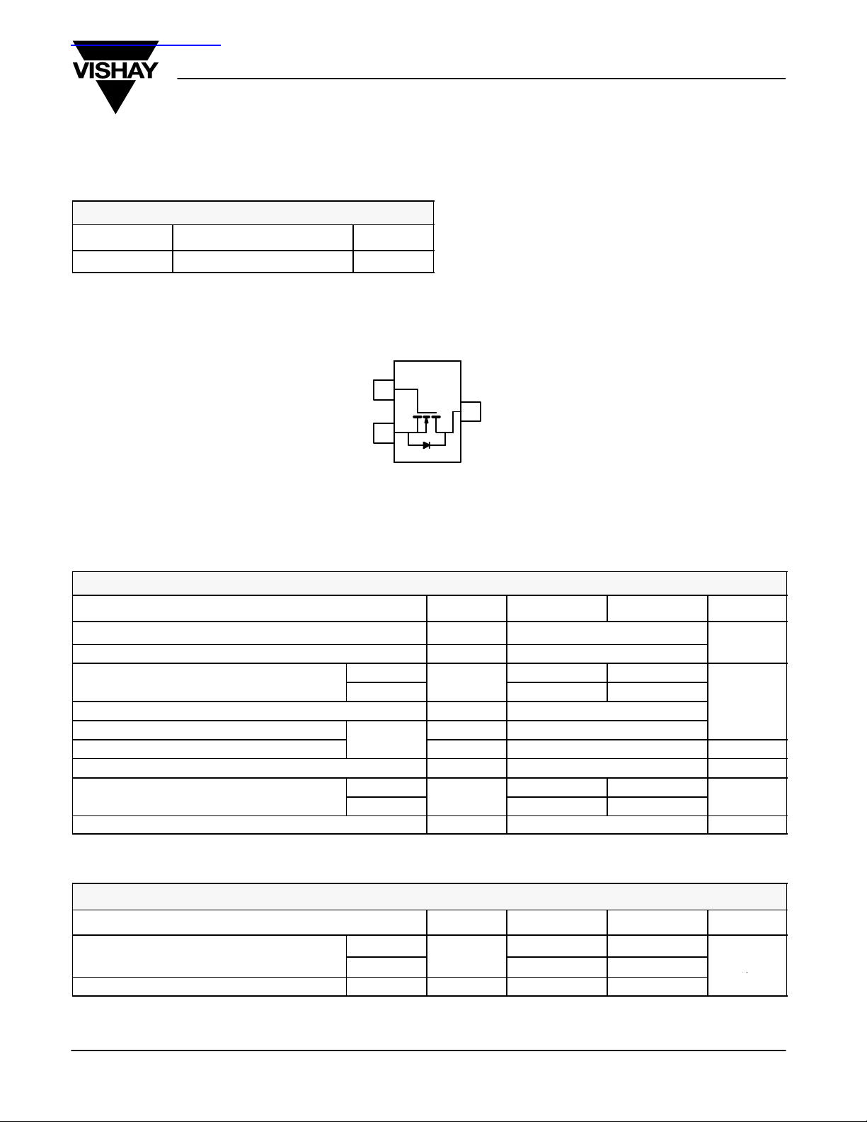
G
S
ID (A)
1
2
TO-236
(SOT-23)
Top View
Si2328DS (D8)*
*Marking Code
D
3
r
DS(on)
(W)
= 10 V 1.5
GS
Vishay Siliconix
ABSOLUTE MAXIMUM RATINGS (TA = 25_C UNLESS OTHERWISE NOTED)
Parameter Symbol 5 sec Steady State Unit
Drain-Source Voltage V
Gate-Source Voltage V
a
Continuous Drain Current (TJ = 150_C)
Pulsed Drain Current
Avalanche Current
Single Avalanche Energy
Continuous Source Current (Diode Conduction)
Power Dissipation
Operating Junction and Storage Temperature Range TJ, T
b
b
a
_
a
TA= 25_C
TA= 70_C
L = 0.1 mH
TA= 25_C
TA= 70_C
I
I
E
P
I
DM
AS
I
DS
GS
D
AS
1.5 1.15
1.2 0.92
S
D
stg
1.25 0.73
0.80 0.47
100
"20
6
6
1.8 mJ
0.6 A
–55 to 150
THERMAL RESISTANCE RATINGS
Parameter Symbol Typical Maximum Unit
Maximum Junction-to-Ambient
Maximum Junction-to-Foot Steady State R
Notes
a. Surface Mounted on 1” x 1” FR4 Board.
b. Pulse width limited by maximum junction temperature
a
t v 5 sec 80 100
Steady State
R
thJA
thJF
130 170
45 55
V
A
W
_C
_C/W
Document Number: 71796
S-05372—Rev. A, 25-Dec-01
www.vishay.com
1
Page 2
Si2328DS
DD
L
W
Vishay Siliconix
New Product
SPECIFICATIONS (TA = 25_C UNLESS OTHERWISE NOTED)
Parameter Symbol Test Conditions Min Typ Max Unit
Static
Drain-Source Breakdown Voltage V(
Gate-Threshold Voltage V
Gate-Body Leakage I
Zero Gate Voltage Drain Current I
On-State Drain Current
Drain-Source On-Resistance
Forward Transconductance
Diode Forward Voltage V
Dynamic
Total Gate Charge Q
Gate-Source Charge Q
Gate-Drain Charge Q
b
a
a
a
BR)DSS
I
r
DS(on)
GS(th)
GSS
DSS
D(on)
g
fs
SD
g
gs
gd
VGS = 0 V, ID = 1 mA 100
VDS = VGS, ID = 250 mA
VDS = 0 V, VGS = "20 V "100 nA
VDS = 80 V, VGS = 0 V 1
VDS = 80 V, VGS = 0 V, TJ = 70_C
VDS w 15 V , VGS = 10 V 6 A
VGS = 10 V, ID = 1.5 A 0.195 0.250
VDS = 15 V, ID = 1.5 A 4 S
IS = 1.0 A, VGS = 0 V 0.8 1.2 V
VDS = 50 V, VGS = 10 V, ID = 1.5 A
Limits
2
75
3.3 4.0
0.47
1.45
V
mA
W
nC
Switching
Turn-On Delay Time t
Rise Time t
Turn-Of f Delay Time t
Fall-Time t
Source-Drain Reverse Recovery Time t
Notes
a. Pulse test: PW v300 ms duty cycle v2%.
b. Guaranteed by design, not subject to production testing.
d(on)
d(off)
r
f
rr
V
= 50 V, R
V
= 50 V, RL = 33
DD
ID ^ 0.2 A, V
GEN
IF = 1.5 A, di/dt = 100 A/ms
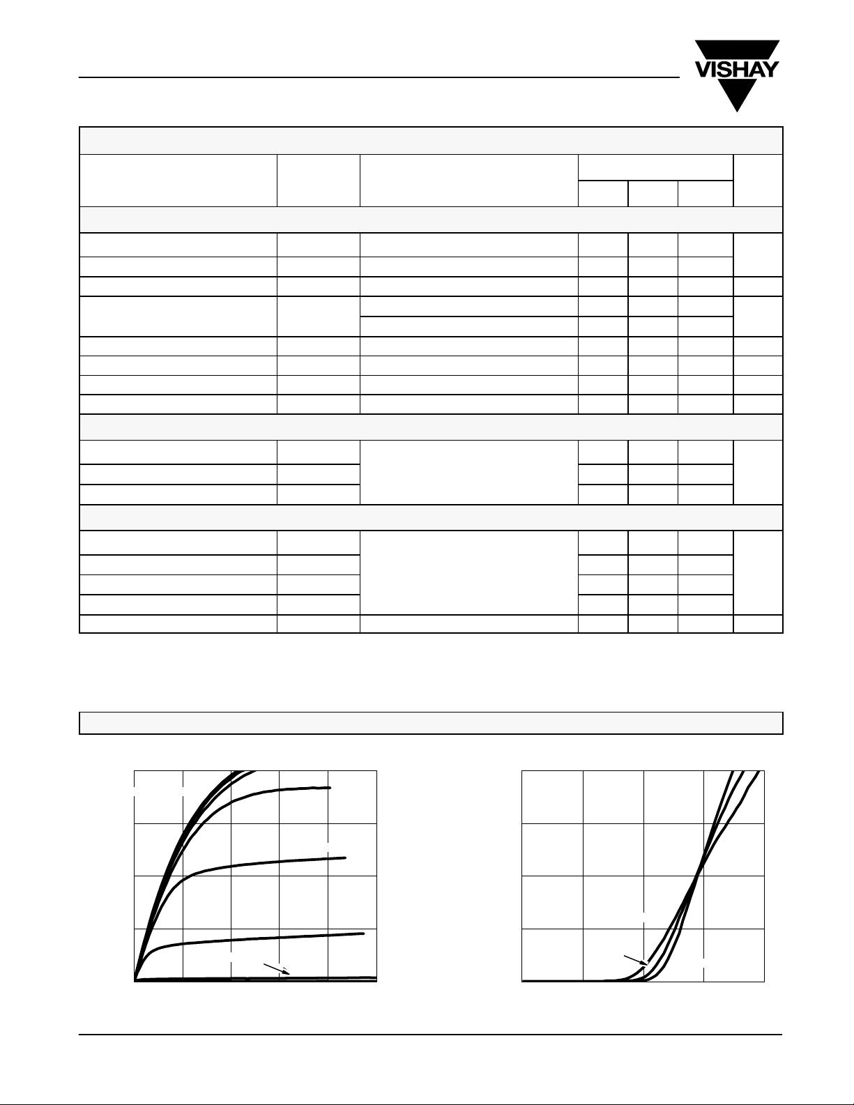
TYPICAL CHARACTERISTICS (25_C UNLESS NOTED)
12
VGS = 10, 9, 8 V
9
6
– Drain Current (A)I
D
3
Output Characteristics Transfer Characteristics
7 V
6 V
5 V
= 33 W
= 10 V, RG = 6 W
12
9
6
– Drain Current (A)I
D
3
TC = 125_C
7 11
11 17
9 15
10 15
50 100 ns
ns
www.vishay.com
2
3, 2, 1 V
0
0246810
VDS – Drain-to-Source Voltage (V)
4 V
25_C
0
02468
VGS – Gate-to-Source Voltage (V)
–55_C
Document Number: 71796
S-05372—Rev. A, 25-Dec-01
Page 3

Si2328DS
New Product
TYPICAL CHARACTERISTICS (25_C UNLESS NOTED)
On-Resistance vs. Drain Current
0.6
0.5
W )
0.4
VGS = 10 V
0.3
– On-Resistance (r
0.2
DS(on)
0.1
0.0
036912
– Drain Current (A)
I
D
Gate Charge
20
VDS = 10 V
= 1.5 A
I
D
16
250
200
150
100
C – Capacitance (pF)
50
C
rss
0
0 20406080100
On-Resistance vs. Junction Temperature
2.5
VGS = 10 V
W)
I
2.0
Vishay Siliconix
Capacitance
C
iss
C
oss
VDS – Drain-to-Source Voltage (V)
= 1.5 A
D
– Gate-to-Source Voltage (V)
GS
V
– Source Current (A)I
0.1
S
12
8
4
0
0123456
Qg – Total Gate Charge (nC)
Source-Drain Diode Forward Voltage On-Resistance vs. Gate-to-Source Voltage
10
1
TJ = 150_C
TJ = 25_C
1.5
(Normalized)
– On-Resistance (r
1.0
DS(on)
0.5
0.0
–50 –25 0 25 50 75 100 125 150
T
– Junction Temperature (_C)
J
0.6
0.5
W )
– On-Resistance (r
DS(on)
ID = 1.5 A
0.4
0.3
0.2
0.1
0.01
0.0 0.2 0.4 0.6 0.8 1.0 1.2
VSD – Source-to-Drain Voltage (V) VGS – Gate-to-Source Voltage (V)
Document Number: 71796
S-05372—Rev. A, 25-Dec-01
0.0
0246810
www.vishay.com
3
Page 4

Si2328DS
Vishay Siliconix
New Product
TYPICAL CHARACTERISTICS (25_C UNLESS NOTED)
Threshold Voltage
0.6
0.3
ID = 250 mA
0.0
–0.3
Variance (V)V
GS(th)
–0.6
–0.9
–1.2
–50 –25 0 25 50 75 100 125 150
TJ – Temperature (_C)
Normalized Thermal Transient Impedance, Junction-to-Ambient
2
12
10
8
6
Power (W)
4
2
0
0.01
Single Pulse Power
TA = 25_C
1
Time (sec)
10
100 6000.1
1
0.1
Thermal Impedance
Normalized Effective Transient
0.01
10
Duty Cycle = 0.5
0.2
0.1
0.05
0.02
–4
Single Pulse
–3
10
Notes:
P
DM
t
1
t
2
t
thJA
thJA
100
1
t
2
(t)
= 176_C/W
1. Duty Cycle, D =
2. Per Unit Base = R
3. TJM – TA = PDMZ
4. Surface Mounted
–2
10
–1
1 10 60010
Square Wave Pulse Duration (sec)
www.vishay.com
4
Document Number: 71796
S-05372—Rev. A, 25-Dec-01
 Loading...