

Page 1
1
Preliminary Information SATURN
SATURN
CDMA/AMPS dual Band IF Receiver for Digital Phones
Preliminary Information
Description
The SATURN circuit is designed for use in dual band dual
mode mobile phones (CDMA/AMPS). The circuit is
designed to be compataible with digital baseband and
mixed signal circuit chips from Mitel (Planet Chip-set)
and Qualcomm (MSM2 and BBA). A wideband AGC
amplifier allows the input of CDMA or AMPS signal paths
with a range power management control options.
Features
● Selectable IF input buffers with characteristic
impedance suitable for interface to IF CDMA and
FM SAW filter outputs
● AGC amplifiers with 90dB of variable gain, fully
compensated for temperature variation
● IQ demodulator with accurately defined output DC
level and low DC offsets
● LO operating at twice frequency with high accuracy
quadrature generation
● Sophisticated power management control operation
● Overload indicator
DS4721 Issue 4.2 April 1999
Odering Information
SATURN/KG/QP1S
SATURN/KG/QP1T
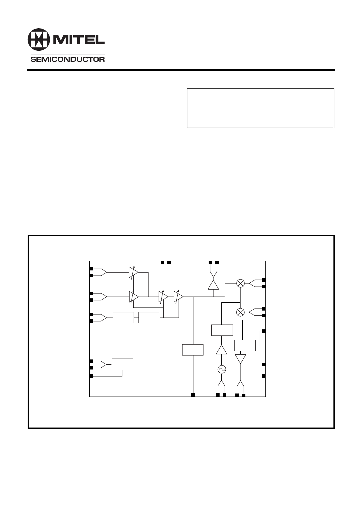
Figure 1 Block diagram
Temperature
Comp.
DLL
I OUT
IF OUT
FM IFIN
Q OU T
Gain
Control
Mode
Control
CDMA IFIN
AGC
STARTUP
ENABLE
MODE CDM
VHF BUF
VHF RES
PRESCALER
Overload
Indicator
OVERLOAD DET
BAND 1900
VHF VCC
VHF VEE
IF VCC
IF VEE
Page 2
2
SATURN Preliminary Information
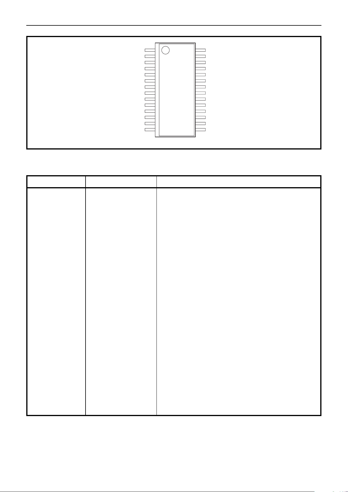
Figure 2 Pin Connections
QSOP28
IF VCC
IF OUTB
IF OUT
IF VEE
GND
CDMA IFIN
CDMA IFINB
FM IFIN
FM IFINB
AGC
AGCB
MODE CDMA
ENABLE
GND
VHF VCC
I OUTB
I OUT
VHF VEE
OVERLOAD DET
VHF RES
VHF RESB
BAND 1900
VHF BUF
VHF BUFB
GND
Q OUT
Q OUTB
STARTUP
Pin Description
Pin No Pin Name Description
1 IF VCC Supply for IF inputs and AGC blocks
2 IF OUTB Post AGC IF output
3 IF OUT Post AGC IF output
4 IF VEE Ground for IF inputs and AGC blocks
5 GND Substrate ground
6 CDMA IFIN Post SAW IF input (CDMA)
7 CDMA IFINB Post SAW IN input (CDMA)
8 FM IFIN Post SAW IF input (FM)
9 FM IFINB Post SAW IF inputs (FM) (AC ground)
10 AGC AGC Control for IF section
11 AGCB AGC control for IF sections (AC ground)
12 MODE CDMA CDMA/FM mode select
13 ENABLE Power up AGC sections of device
14 GND Substrate Ground
15 STARTUP Power up Oscillator, DLL and Mixer sections of the device
16 QOUTB Q channel baseband output
17 OUT Q Channel baseband output
18 GND Ground
19 VHF BUFB VHF oscillator buffered output for synthesiser
20 VHF BUF VHF oscillator buffered output for synthesiser
21 BAND 1900 VHF oscillator tuning band select input
22 VHF RESB VHF VCO resonator
23 VHF RES VHF VCO resonator
24 OVERLOAD DET Overload detector output
25 VHF VEE Ground for VHF VCO and DLL blocks
26 I OUT I channel baseband output
27 I OUTB I channel baseband output
28 VHF VCC Supply for VHF and DLL blocks
Page 3
3
Preliminary Information SATURN
Electrical Characteristics (Mode Control)
Description ENAVLE STARTUP MODE CDMA BAND 1900 Conditions
Standby Mode 0 0 X X All circuits powered down
except logic inputs
Start up Mode 0 1 X 1 For high band IF
(210.38MHz)
0 1 X 0 For low band IF (85.38MHz)
Turns on VCO circuits, DLL
quadrature generation,
prescaler and IQ
demodulator. All other
circuits remain powered
down
CDMA mode 1 1 1 1 For high band IF
(210.38MHz)
1 1 1 0 For low band IF (85.38MHz)
All circuits operational
except for IF output buffer,
CDMA input stage selected.
FM Mode 1 1 0 0 All circuits operational
except for IF output buffer,
FM input stage selected.
Alternative FM mode 1 1 0 1 Note 4
CDMA IF AGC 1 0 1 X Demodulator and LO
only mode generation circuitry powered
down. IF output buffer
enabled
FM IF AGC 1 0 0 X Demodulator and LO
generation circuitry powered
down. IF output buffer
enabled.
X = Don’t Care
Notes
1. STARTUP mode is provided to allow VCO/DLL/prescalers to stabilise before signal path is activated. This is a power-saving
feature since the signal path is redundant during this period. If this feature is not required, the ENABLE and STARTUP
control pins can be shorted together so that all circuitry is activated at the same time.
2. In high band mode (Band 1900 = 1) the VCO operates at twice the IF frequency. For example if IF = 210.38MHz then the
oscillator operates at 420.76MHz. A delay locked loop (DLL) circuit then generates the quadrature LO signals. The prescaler
output, VHFBUF, is VCO frequency divided by 8 (52.494MHz).
3. In low band mode (Band 1900 = 0) the VCO operates at 4 times the IF frequency. for example if IF = 85.38MHz the oscillator
operates at 341.52MHz. This is then divided and uses DLL circuit to provide the quadrature LO signals. The prescaler output,
VHFBUF, is VCO frequency divided by 8 (42.69MHz).
4 This mode can be used for FM. The VCO operates at twice the LO frequency. This mode is not normally used as a large
tuning range is required on the VCO. Prescaler output is LO frequency divided by four.
Page 4

4
SATURN Preliminary Information
Electrical Characteristics (DC specifications)
T
amb
= 30°C to +70°C, V
cc
= +2.7 to +3.6. These characteristics are guaranteed by either production test or design.
They apply within the specified ambient temperature and supply voltage unless otherwise stated.
Characteristic Value Units Conditions
Min Typ Max
General
Supply Voltage 2.7 3.0 3.6 V All Vcc Pins
Operating temperature -30 27 85 °C Ambient See note 1
Current Consumption
Standby Mode 0.03 0.1 mA
Startup Mode 8 13 mA
CDMA Mode 14 23 mA
FM Mode 14 23 mA
CDMA AGC only Mode 8 13 mA
FM AGC only Mode 11 18 mA
Mode Control Logic
CMOS input logiv high, VIH Vcc-0.5 Vcc+0.1 V All logic inputs
CMOS input high current, IIH -10 10 µA All logic inputs
CMOS input low current, IIL -10 10 µA All logic inputs
Switching time between any two Modes 3 ms
AGC Control 0.1 2.6 V
AGC Input impedance 100 130 160 kΩ
DC Common Mode voltages
I OUT, I OUTB (CDMA Mode) Vcc-0.8 Vcc-0.6 Vcc-0.4 V
I OUTB, QOUTB
I OUT< Q OUT (FM Mode) Vcc-0.8 Vcc-0.6 Vcc-0.4 V
I OUTB, Q OUTB
Note 1. Specifications are guaranteed over -30 to + 70°C, however operation is guaranteed over the extended range
of -30 to +85°C with minimal variation in specified parameters.
Absolute Limits
Description Min Typ Max Units Comments
Supply Voltage 4.0 Volts
Operation temperature, Tamb -30 +85 °C Ambient temperature
Storage temperature, Tstg -40 +125 °C
Junction temperature, Tj -30 +125 °C
Power dissipation 350 mW
Maximum Pin Voltage Vcc+0.6 Volts All pins except Vcc and GND
Minimum Pin Voltage -0.6 Volts All pins except Vcc and GND
ESD voltage 1.75 kV Human Body Model
Page 5

5
Preliminary Information SATURN
Electrical Characteristics (AC specifications) Continued
T
amb
= 30°C to +70°C, V
cc
= +2.7 to +3.6. These characteristics are guaranteed by either production test or design.
They apply within the specified ambient temperature and supply voltage unless otherwise stated.
Frequency = 210.38MHz
Characteristic Value Units Conditions
Min Typ Max
CDMA AGC
Max Voltage Gain to demodulator 48 50 dB To demodulator outputs
output
Min Voltage Gain to demodulator -55 -47 dB To demodulator
output
Max Voltage Gain to IF buffer output 42 -43 dB IF AGC only mode
Min voltage Gain to IF buffer output -51 -49 dB IF AGC only mode
AGC control Max 2.6 V Gain = Gain max
AGC control Min 0.1 V Gain = Gain min
Gain slope 40 dB/V
Gain slope linearity 6 90 dB/V Over gain control range
Gain temperature stability -2 2 dB
Channel gain variation -0.1 0.1 dB Within channel bandwidth
@ 210.38MHz
NF
Gainmax
5.5 6.5 dB Rs (500Ω)
Input V1dB
Gainmin
110 dBµV Minimum gain
104 dBµV Power (500Ω)
IIP3
Gainmin
114 120 dBµV Minimum gain
Input impedance 500 Ω With addition of external
resistor across IF inputs
IF Frequency 50 250 MHz
CDMA to Amps isolation 30 dB
Page 6

6
SATURN Preliminary Information
Electrical Characteristics (AC specifications) Continued
T
amb
= 30°C to +70°C, V
cc
= +2.7 to +3.6. These characteristics are guaranteed by either production test or design.
They apply within the specified ambient temperature and supply voltage unless otherwise stated.
Frequency = 85.38MHz
Characteristic Value Units Conditions
Min Typ Max
FM AGC
Max Voltage Gain to demodulator 52 54 dB To demodulator outputs
output
Min Voltage Gain to demodulator -49 -47 dB To demodulator
output
Max Voltage Gain to OF buffer output 54 59 dB IF AGC only mode
Min voltage Gain to IF buffer output -48 -42 dB IF AGC only mode
AGC control Max 2.6 V Gain = Gain max
AGC control Min 0.1 V Gain = Gain min
Gain slope 40 dB/V
Gain slope linearity 6 80 dB/V Over gain control range
Gain temperature stability -2 2 dB For any gain setting
NF
Gainmax
6 dB 850Ω source
Input V1dB
Gainmin
98 105 dBµV Minimum gain
IIP3
Gainmin
103 113 dBµV Minimum gain
Input Impedance 850 Ω With addition of external
resistor across IF inputs
IF Frequency 50 250 MHz
VHF Local Oscillator
Quaderature generation
LO input Frequency 100 500 MHz
VCO Phase noise -100 -98 dBc/Hz @30kHz, Hiband mode
Minimum tank Q=15 Note 1
VCO Noise floor -130 dBc/Hz @>3MHz, Note 1
VCO buffer output 350 mV pk-pk single ended
VCO buffer output impedance 100 Ω Differential
Note 1: Phase noise is specified at the LO input to the mixers.
Page 7

7
Preliminary Information SATURN
Electrical Characteristics (AC specifications) Continued
T
amb
= 30°C to +70°C, V
cc
= +2.7 to +3.6. These characteristics are guaranteed by either production test or design.
They apply within the specified ambient temperature and supply voltage unless otherwise stated.
Characteristic Value Units Conditions
Min Typ Max
Demodulator Output I OUT, I OUTB, Q OUT, Q OUTB
I/Q Gain matching 0.1 0.25 dB
I/Q Phase matching 0.5 2 deg
Output impedance 3 4 5 kΩ Differential
Baseband Bandwidth 50 MHz Defined by on-chip first order
low-pass filter
Output IP3 117 119 dBµV
Baseband differential DC offset 3.5 mV
Overload Detect Referred to baseband outputs
CDMA Mode 104 dBµV
FM Mode 106 dBµV
Page 8

Page 9

M Mitel (design) and ST-BUS are registered trademarks of MITEL Corporation
Mitel Semiconductor is an ISO 9001 Registered Company
Copyright 1999 MITEL Corporation
All Rights Reserved
Printed in CANADA
TECHNICAL DOCUMENTATION - NOT FOR RESALE
World Headquarters - Canada
Tel: +1 (613) 592 2122
Fax: +1 (613) 592 6909
North America Asia/Pacific Europe, Middle East,
Tel: +1 (770) 486 0194 Tel: +65 333 6193 and Africa (EMEA)
Fax: +1 (770) 631 8213 Fax: +65 333 6192 Tel: +44 (0) 1793 518528
Fax: +44 (0) 1793 518581
http://www.mitelsemi.com
Information relating to products and services furnished herein by Mitel Corporation or its subsidiaries (collectively “Mitel”) is believed to be reliable. However, Mitel assumes no
liability for errors that may appear in this publication, or for liability otherwise arising from the application or use of any such information, product or service or for any infringement of
patents or other intellectual property rights owned by third parties which may result from such application or use. Neither the supply of such information or purchase of product or
service conveys any license, either express or implied, under patents or other intellectual property rights owned by Mitel or licensed from third parties by Mitel, whatsoever.
Purchasers of products are also hereby notified that the use of product in certain ways or in combination with Mitel, or non-Mitel furnished goods or services may infringe patents or
other intellectual property rights owned by Mitel.
This publication is issued to provide information only and (unless agreed by Mitel in writing) may not be used, applied or reproduced for any pur pose nor form par t of any order or
contract nor to be regarded as a representation relating to the products or services concerned. The products, their specifications, services and other information appearing in this
publication are subject to change by Mitel without notice. No warranty or guarantee express or implied is made regarding the capability, performance or suitability of any product or
service. Information concerning possible methods of use is provided as a guide only and does not constitute any guarantee that such methods of use will be satisfactory in a specific
piece of equipment. It is the user’s responsibility to fully determine the performance and suitability of any equipment using such information and to ensure that any publication or
data used is up to date and has not been superseded. Manufacturing does not necessarily include testing of all functions or parameters. These products are not suitable for use in
any medical products whose failure to perform may result in significant injury or death to the user. All products and materials are sold and services provided subject to Mitel’s
conditions of sale which are available on request.
 Loading...