

Page 1

SAN2202
sames
sames
samessames
APPLICATION NOTE
SINGLE CHIP “SPEAKERPHONE” WITH
8 - OHM LOUDSPEAKER AMPLIFIER
1 Scope
This application note describes a low-cost add-on cir c uit f or dr iving an 8Ω-Loudspeaker to get a sim ple loudhearing
(“Speakerphone”) Telephone.
To possible ways of supplying the amplifier are shown:
SAN2202a: Amplifier supply in shunt transistor path
SAN2202b: Amplifier supply by power extraction circuit (SAN3020)
It can be added to any SA253x application without interfering with PTT-r elevant parameters, like AC-impedance,
Sidetone cancellation or DC-mask.
2 Key Features
•
Low cost additional circuit enables use of loudhearing function
•
Full duplex “handsfree” operation via handset microphone and loudspeaker (at distances <2m between
telephone and user)
•
Can be added to any SA253x- application
•
Enables use of low cost 8Ω - Loudspeaker
•
High output power with low distortion
•
Entirely powered from the telephone line
•
No influence of loudspeaker amplifier in AC-impedance, sidetone cancellation or DC-mask
•
Loudspeaker volume adjustable by potentiometer
•
Excellent sidetone cancellation of SAS253x circuits enables high loudspeaker volume without howling between
handset microphone and loudspeaker
SAN2202 PDS038-SA2531/2-001 Rev. B 21-03-00
Page 2

SAN2202
TABLE OF CONTENTS
1 SCOPE.............................................................................................................................................................................................................1
2 KEY FEATURES..............................................................................................................................................................................................1
3 OTHER APPLICABLE DOCUMENTS AND PAPERS......................................................................................................................................3
4 REVISION STATUS .........................................................................................................................................................................................3
5 GENERAL DESCRIPTION...............................................................................................................................................................................3
MPLIFIER SUPPLY
5.1 A
6 BLOCK DIAGRAM...........................................................................................................................................................................................4
HOW TO AVOID HOWLING
6.1
7 CIRCUIT DESCRIPTION..................................................................................................................................................................................5
LOUDSPEAKER AMPLIFIER
7.1 8Ω
MPLIFIER SUPPLY IN SHUNT TRANSISTOR PATH
7.2 A
MPLIFIER SUPPLY BY POWER EXTRACTION CIRCUIT
7.3 A
8 MEASUREMENT RESULTS & CURVES.........................................................................................................................................................6
REQUENCY RESPONSE
8.1 F
MAXIMUM SENDING LEVEL
8.2
MAXIMUM OUTPUT POWER
8.3
N-RESISTANCE IN PULSE DIALING
8.4 O
9 APPLICATION SCHEMATIC ............................................................................................................................................................................8
10 LIABILITY AND COPYRIGHT STATEMENT ..................................................................................................................................................9
OMPARISON OF
: C
SAN2202
A AND
SAN2202B:..............................................................................................................3
.............................................................................................................................................................................4
.......................................................................................................................................................................5
............................................................................................................................................5
SAN3020 ......................................................................................................................5
..............................................................................................................................................................................6
............................................................................................................................................................................6
...........................................................................................................................................................................6
...............................................................................................................................................................7
2/9
same s
same s
same ssame s
Page 3
SAN2202
3 Other applicable documents and papers
1. Data Sheet SA2531/2 Single Chip Telephone
2. Application Note SAN3020: Power extraction for external loads
4 Revision status
SAN2202 Application Note (this document)
5 General description
The amplifier is a simple, low cost add-on circuit to the SA253x s ingle chip telephone family. It is supplied by the
line current and amplifies the receive signal, taken from either RO1 or RO2 (Receive outputs), see Fig.1.
Compared to more complex “real” handsfree circuits there is no channel switching or anti-larsen circuit
implemented, therefore the receive and transmit gains must be lower to avoid howling.
However, at short distances between user and telephone (<2m , which is adequate for nor mal of fice work ) there is
even full duplex “handsfree” operation possible, when the handset is placed next to the telephone with the
microphone facing to the user.
Due to the excellent sidetone cancellation of the SA253x circuits, howling between handset microphone and
loudspeaker will only occur, when both are put very close to each other. In norm al operation, no howling will oc cur,
even with maximum loudspeaker volume.
Due to the unique structure of the SA253x family’s line adaption, adding the amplifier has no influence on the
important PTT related parameters, like AC-impedance, DC-mask, etc. (see Pt. 5.1 below).
Note: all subsequent component numbering refers to the schemat i c, shown in Pt. 9
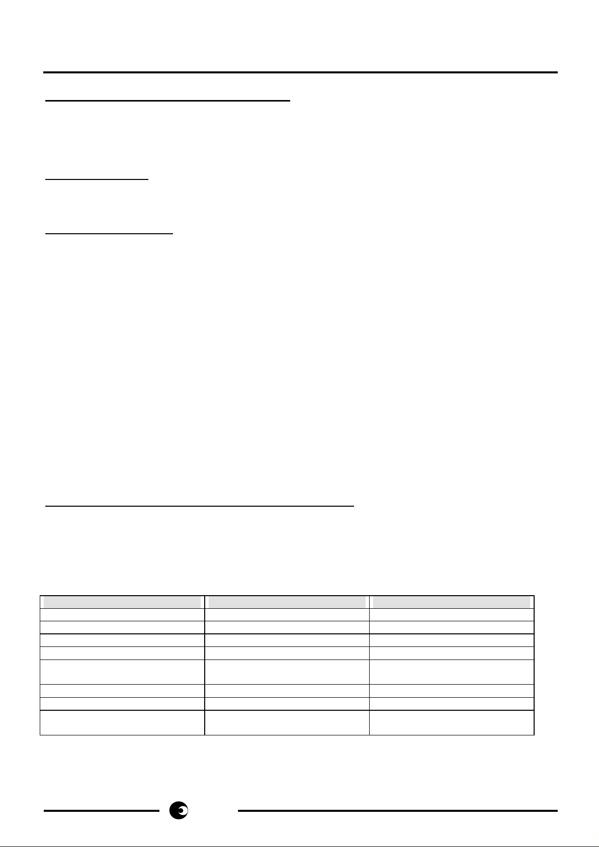
5.1 Amplifier supply: Comparison of SAN2202a and SAN2202b:
The following table describes the difference between the two types of amplifier supply: while the simple SAN2202a
supply shows slight influence in maximum sending level and “Make”-resistance in pulse dialing , the SAN2202b (3
extra components) s upply has no influence in these parameters and has a m ore stable maximum output driving
capability at high line currents (see Fig.4 & 5).
Parameter SAN2202a (Shunt path supply) SAN2202b (Power extraction)
AC impedance no influence no influence
off -hook DC mask no influence no influence
Tx-/Rx-gains no influence no influence
“Make”-resistance in pul se dialing
max. sending level
(soft clip level = 4Vpp)
<4Vpp for I
max. 8Ω output power; THD <2%
max. 8Ω output power; THD <3%
number of extra components none 3parts:
<230Ω @ 20mA <160Ω @20mA
no influence for I
>40mA (see.Fig.3)
Line
≈
26mW
≈
32mW
<40mA
Line
no influence ; soft clip level
1 transistor,1diode,1resistor
≈
27mW
≈
34mW
3/9
sames
sames
samessames
Page 4
SAN2202
6 Block diagram
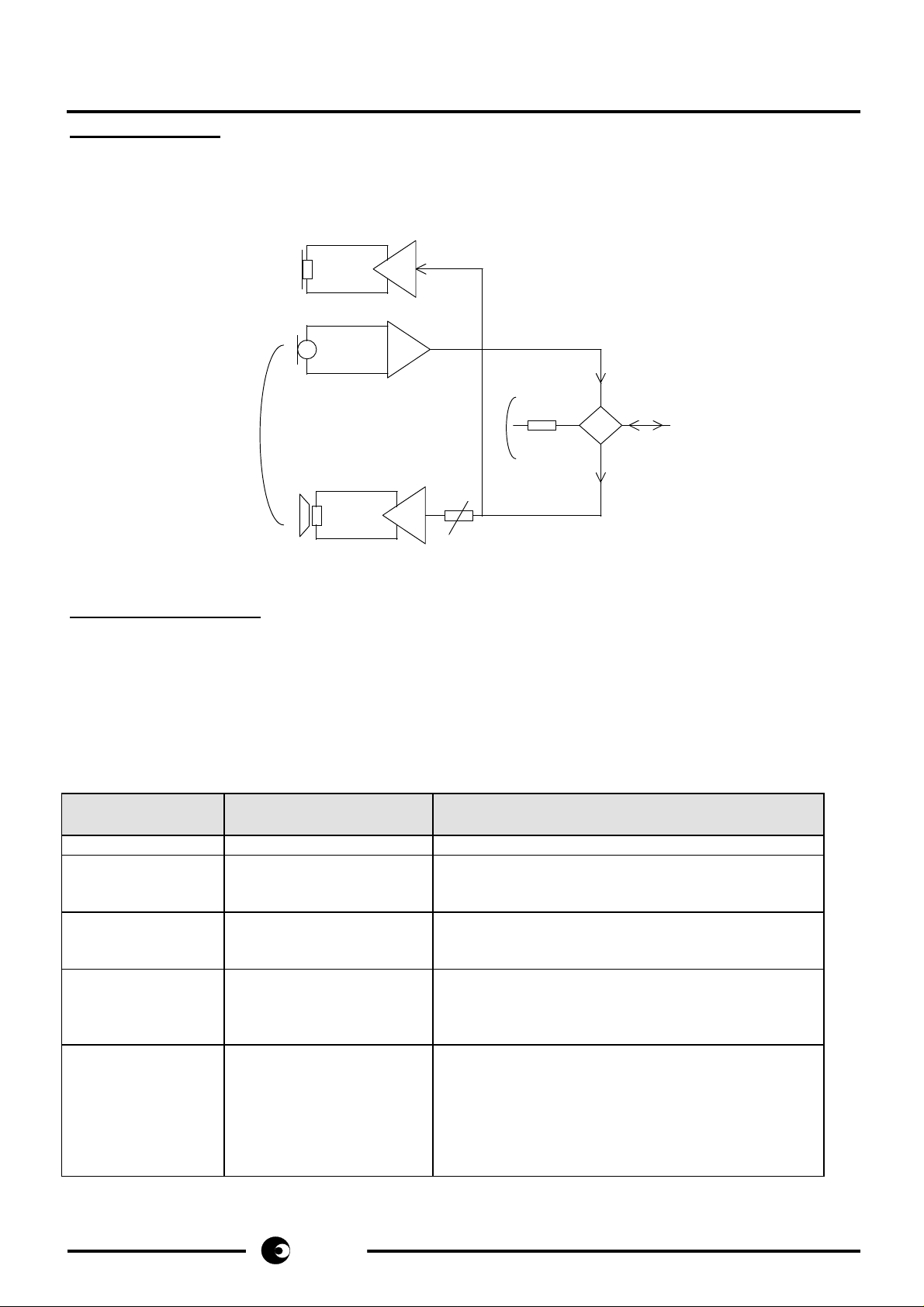
Fig. 1 shows the block diagram of the speech paths: the transmitted signal is fed to the line via the 2-4 wire
interface and the receive signal coming from line is fed to the Rx amplifier. The same Rx signal passes an
attenuator for volume control and is then amplified by the loudspeaker amplifier.
RX
Amplfier
Handset
TX
Amplfier
Acoustic feedback
LS
Amplfier
manual volume control
Transmit path
Sidetonet
Receive path
Z ACr
2-4
wire
interface
Line
Fig. 1: speakerphone block diagram
6.1 how to avoid howling
As can be seen on Fig.1, there is an acoustic loop from
loudspeaker ⇒ acoustic feedback (determined by the mechanical distance between loudspeaker and handset
microphone ⇒ Tx amplifier ⇒ sidetone ⇒ LS amplifier.
Howling will occur, when the total loop gain is ≥1 ( equal to ≥ 0dB) . Therefore the following conditions will have an
effect in loop gain:
Parameter: measure to reduce
howling
Transmit gain reduce gain must meet the SLR limits
Sidetone increase sidetone
cancellation
Loudspeaker volume decrease loudspeaker
volume
Loudspeaker
limit bandwidth howling will occur with the frequency of the highest
frequency response
acoustic coupling
between
loudspeaker and
increase distance between
loudspeaker and handset
microphone
handset microphone
4/9
sames
sames
samessames
can be done by optimizing the sidetone network, the
better the sidetone cancellation, the more gain can be
given to the loudspeaker
for good performance, a maximum of loudspeaker
volume is desirable, therefore this should be the least
step
amplification. Therefore the frequency response curve
should be as flat as possible and limited to the speech
band (≈ 300..3400Hz)
In normal operation, the distance can be down to a
few centimeters, when the handset is put onto or off
the cradle. The loop should be adjusted such that in
normal speech mode there is no howling at distances
>5..10 cm. Additionally, the loudspeaker can be
mounted away from the handset microphone position,
like on the side or on the rear, if possible.
Note:
Page 5

SAN2202
7 Circuit description
7.1 8
loudspeaker amplifier
ΩΩΩΩ
The amplifier is a simple Class-A type amplifier. Gain is set by R6, the bandwidth is imited by CC4 (to avoid
howling). Q4 and Q6 should be matched in gain (complementary types).
Nearly all the line current will flow through these transistors, independent of the signal output amplitude. The
maximum power dissipation of Q4 and Q6 is
P
where: V
V
CE,Q4
CE,Q6
= V
= V
BE,Q4+UD2
BE,Q6+UD1
and
= VCE * (I
tot
Line
- I
IC1
)
VBE(Q4,Q6) ≈ 0.7V, VTH(D2,D1) ≈ 0.52V.
I
Power dissipation at I
In order to maintain no interferenc e of the circuit to AC-im pedance, DC-mas k, maxim um sending level, etc..., the
amplifiers´ supply voltage V
= typ. 3mA (see data sheet)
SA2531/2
=100mA:
line
= (0.7+0.52) * (0.1-0.003) = 118mW
P
tot
must be limited to <2.44V
CC
1)
.
This is accomplished by
V
= VBE(Q6) + VTH(D1)+ VTH(D2)+VBE(Q4) .
CC
V
= 0.68V + 0.5V + 0.5V + 0.68V =
CC
1)
Critical for SAN2202a configuration, not critical for SAN2202b configuration.
VLI can range between 2.5...6.5V ⇒ 4.5V ± 2V
(max. sending level),
peak
2.36V
the C-E saturation voltage of Q3 is assumed >60mV
To maintain full transmit swing (± 2V
) ⇒ VC(Q3) = VCC =(2.5V-60mV) <
peak
2.44V
Transistor Q1,R1,R2 and R3 forms an impedance matching circuit to provide better matching between the receive
output of the IC and the output amplifier stage.
7.2 Amplifier supply in shunt transistor path
This configuration requires no extra components. However, the maximum voltage of VPP must be considered: If V
PP
rises >2.44V, the maximum transmit level will be slightly distorted at the negative half-wave.
Additionally, the “Make”-resistance in pulse dialing will be higher, because with CS being pulled to V
be shorted to V
(as in the standard application AN1500 with the collector of Q3 being connected to VSS).
BE
SS
, V
cannot
LI
During pulse dialing, VLI will be ≈2.5V, thus increasing the total “ON”-resistance by
..
VV
25 06
∆ΩΩ
R
ON
−
=
ImA
3
−
Line
=
111 20 196 100
mA mA
( ).... . ( )
7.3 Amplifier supply by power extraction circuit SAN3020
This power extraction can be used to supply any external load by the available line current without affecting the
performance of the s ingle ch ip telephone. A detailed desc r iption of this cir cuit is given in applic ation note SAN3020.
“ON”-resistance in pulse dialing (compared to the standard application AN1500) is only increased by ≈10Ω (see.
Fig. 6).
5/9
sames
sames
samessames
Page 6
SAN2202
8 Measurement results & curves
8.1 Frequency response
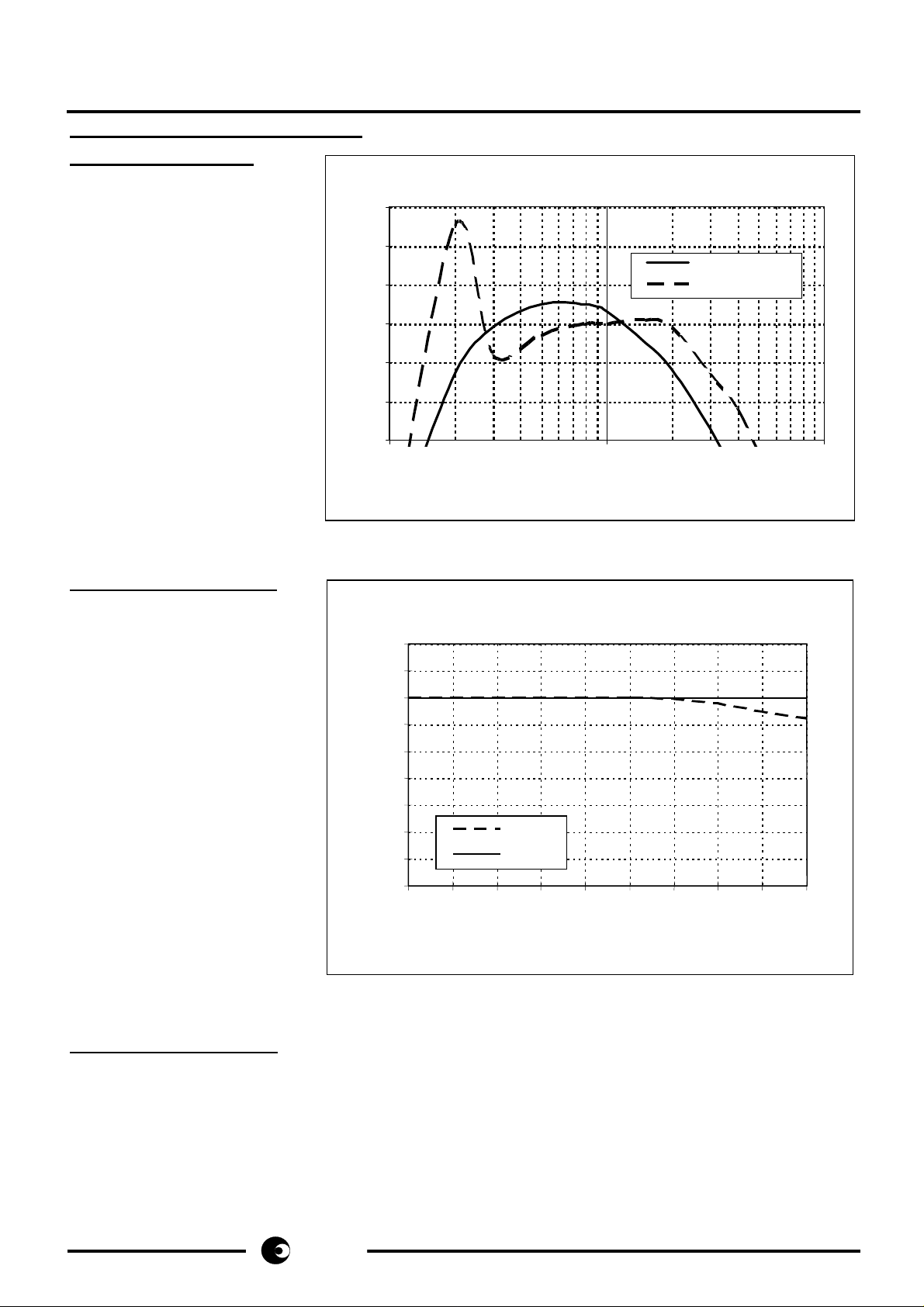
Fig. 2 shows the frequency
response curve of the loudspeaker
amplifier. The curve shows the
output level on an 8Ω resistor
(solid line) and an 8Ω loudspeaker
(dotted line; PHILIPS AD3371
series 80mm∅ 8Ω speaker)
measured with maximum volume
and
-10dBm Rx level on line. The peak
at 200Hz is a resonant frequency
of the specific loudspeaker type.
Gain of the amplifier is set by the
resistors R6 and the attenuation of
VR1. The bandwidth is adjusted by
CC4.
Frequency response of LS-Amplifier
-12
-13
8 Ohm R esistor
-14
-15
-16
Output level [dBm]
-17
-18
100 1000 10000
f [H z]
8 Ohm Loudspeaker
8.2 maximum sending level
Fig.3 shows the maximum
Transmit sending level, measured
at LI vs. line current, assuming a
total harmonic distortion (THD) of
less than 1%.
AN2201a (dotted line):
At line
currents >40mA, VPP will rise up to
2.5V (@ 90mA) and sending level
will be slightly distorted before it
reaches the soft clip level (± 2V
peak
) .
AN2202b (solid line):
There is no
influence in maximum sending
level, the transmit signal can be up
to the soft clip level at line currents
of >12mA.
Fig. 2:Frequency response of loudspeaker amplifier (P
max. sending level @ THD < 1%
4,4
4,2
4
3,8
3,6
3,4
3,2
VLI [Vp p]
3
2,8
2,6
15 20 25 30 35 40 45 50 55 60
SAN2202a
SAN2202b
Line current [mA]
=-10dBm)
Line
Fig. 3: maximum sending level vs. line current (@ THD <1%)
8.3 maximum output power
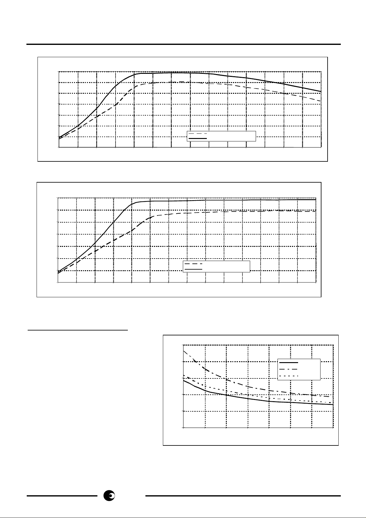
Fig.4 and Fig.5 show the maximum output power on an 8Ω loudspeaker at f=1kHz: the curves indicate the
maximum output power with <2% and <3% total harmonic distortion.
SAN2202a:
The lower output drive capability at higher line currents results from nonlinearities at higher collector
currents and mismatch in the complementary transistor types.
SAN2202b:
6/9
Maximum output power is not decreased with higher line currents.
sames
sames
samessames
Page 7
SAN2202
p
p
@
8 Ohms
owe r
ut
[mWrms]
LS out
SAN2202a: LS output power vs. line current
35
30
25
20
15
10
5
0
15 20 25 30 35 40 45 50 55 60 65 70 75 80 85
line current [mA]
Pmax [mW], THD<2%
Pmax [mW], THD<3%
Fig. 4: SAN2202a: maximum output power on 8Ω loudspeaker vs. line current, f=1kHz
SAN2202b: LS output power vs. line current
35
30
25
20
[mWrms]
15
10
LS output power @8Ohms
5
0
15 20 25 30 35 40 45 50 55 60 65 70 75 80 85
Fig. 5: SAN2202b: maximum output power on 8
8.4 On-resistance in pulse dialing
As described in Pt. 7.2 and 7.3, the ONresistance (=“Make”-resistance) in both
applications is higher than with the standard
application, AN1500. However, the ONresistance in pulse dialing is generally low with
SA253x - applications, this param eter allows a
wide tolerance to meet the PTT specs.
Germany’s BAPT223 ZV5, for exam ple, allows
RON ≤ 390Ω @ I
>24mA.
Line
Fig. 6 shows the ON-resistance ,meas ured on
a-and b-terminals in pulse dialing with the
SAN2202 applications compared to the
standard application SAN2201.
Note: since the measurem ent is taken at a- and
b-terminals, the overall resistance including
ON-resistance of line-transistor) will be
measured.
Pmax [mW], THD<2%
Pmax [mW], THD<3%
line current [mA]
loudspeaker vs. line current,f=1kHz
Ω
On-resistance in pulse dialing
250
200
150
100
a-b resistance [Ohms]
50
0
20 30 40 50 60 70 80 90
line current [mA]
AN1500
SAN2202a
SAN2202b
Fig. 6:On-resistance in pulse dialing with SAN2201,SAN2202a and -b
7/9
sames
sames
samessames
Page 8
SAN2202
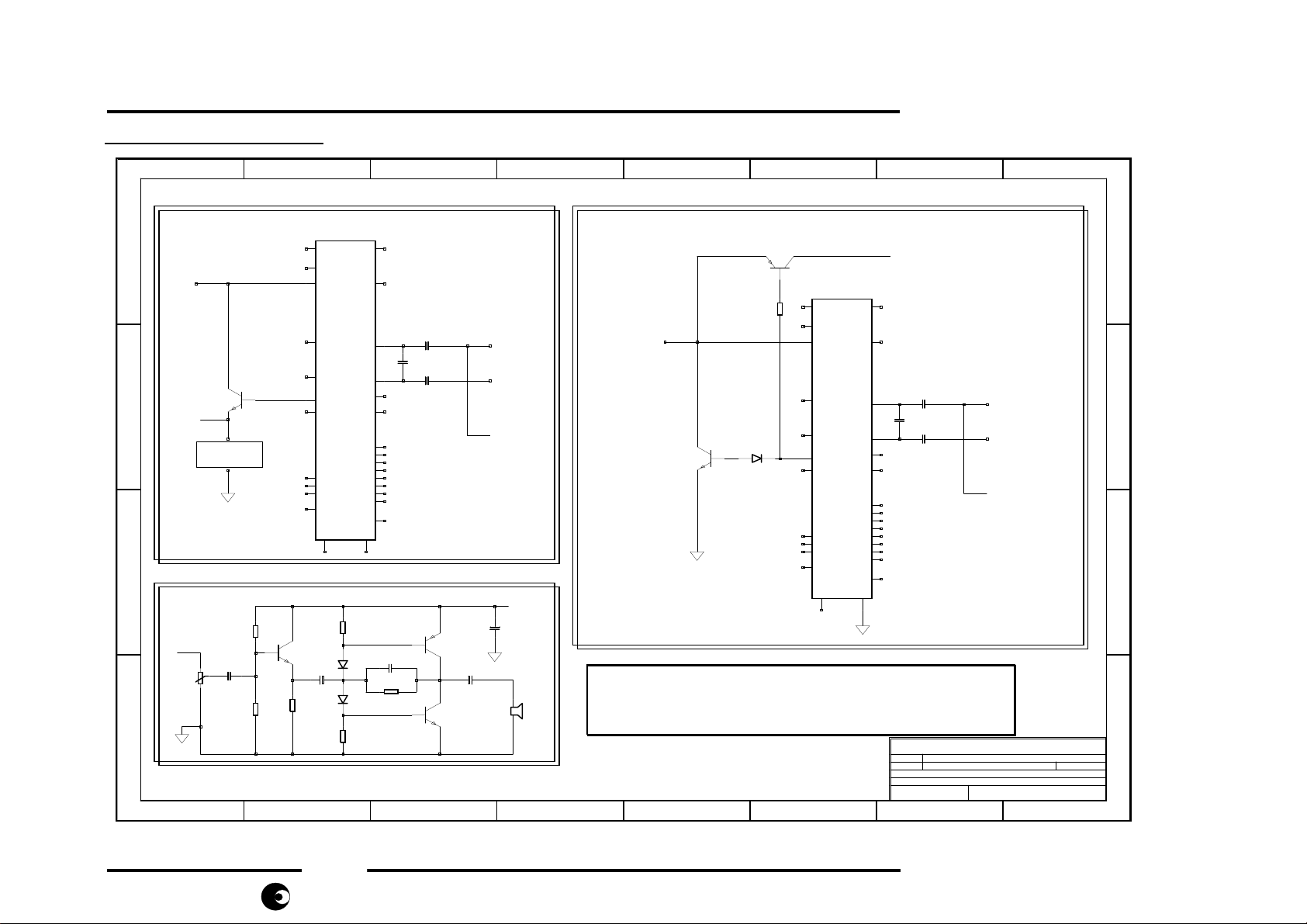
9 Application schematic
1 2 3 4 5 6 7 8
Amplifier supply in shunt transistor path
A
Q3
B
vpp
BC327
Power to
speaker amp
C
8 Ohm Loudspeaker Amplifier
R1
47K
vin
VR1
50K
CC1
270nF
R2
47K
D
1 2 3 4 5 6 7 8
Q1
BC337-10
R3
1K
21
1
27
28
6
25
7
10
8
22
9
FCI
LS
LI
IC1
RI
STB
AGND
CS
SA2531/2
CI RR
HS/DP
MO
MODE
LLC
VDD
R4
22K
D1
CC2
10U
+
D2
R5
22K
RO1
RO2
OSC
SAN2202BSAN2202A
Amplifier supply by power extraction circuit SAN3020
23
M1
Q5
BC327-40
24
M2
21
FCI
5K1
R7
LS
1
27
2
3
5
12
16
C1
15
C2
14
C3
13
C4
20
R1
19
R2
18
R3
17
R4
11
VSS
264
C12
10u
C11
X
10u
C13
vin
BC327
Q2
D3
LI
28
RI
6
STB
25
CS
7
CI RR
10
HS/DP
8
MO
22
MODE
9
LLC
I_96
SA2531/2
VDD
vpp
+
CC5
470U
CC3
100U
+
SP1
8 Ohm
The information furnished here by SAMES is believed to be correct and accurate. However, SAMES shall not
be held liable to any party for any damages including but not limited to personal injury, property damage, loss of
profits, loss of use, interuption of business or indirect, special, incidental or consequential damages, of any kind,
in connection with or arising out of the furnishing, performance or use of the technical data. No obligation or
liability to any third party shall arise or flow out of SAMES rendering technical or other services.
CC4
R6
47nF
5K1
Q6
BC327-40
Q4
BC337-40
vpp
23
M1
24
M2
2
RO1
CC6
X
3
RO2
5
AGND
12
16
C1
15
C2
14
C3
13
C4
20
R1
19
R2
18
R3
17
R4
11
OSC
VSS
264
SAMES Telecom
Sch.
Pn#
Single Chip Telephone Application Circuit
Sh
CC7
CC8
01 01
10u
10u
SAN2202
vin
Rev :
3rd March 1997Date :of
A
B
C
D
1.1
8/9
sames
sames
samessames
Page 9

SAN2202
10 Liability and Copyright Statement
Disclaimer:
Micro-Electronic Systems ( Pty) Ltd ("SAMES”) and may not be copied or disclosed to a third party, in whole or in
part, without the express written consent of SAMES. The information contained herein is cur rent as of the date of
publication; however, delivery of this document shall not under any circumstanc es create any implication that the
information contained herein is correct as of any time subsequent to such date. SAMES does not undertake to
inform any recipient of this document of any changes in the inform ation contained herein, and SAMES expressly
reserves the right to make changes in such information, without notification,even if such changes would render
information contained herein inaccurate or incomplete. SAMES makes no representation or warranty that any
circuit designed by reference to the information contained herein, will function without errors and as intended by the
designer
.
The information contained in this document is confidential and proprietary to South African
South African Micro-Electronic Systems (Pty) Ltd
P O Box 15888, 33 Eland Street,
Lynn East, Koedoespoort Industrial Area,
0039 Pretoria,
Republic of South Africa, Republic of South Africa
Tel: 012 333-6021 Tel: Int +27 12 333-6021
Fax: 012 333-3158 Fax: I nt +27 12 333- 3158
W eb Site : http://www.sames.co.za
9/9
sames
sames
samessames
 Loading...