

Page 1
SAN3020
sames
sames
samessames
APPLICATION NOTE
SINGLE CHIP TELEPHONE POWER
EXTRACTION FOR EXTERNAL LOADS
1 Scope
This application note describes a simple add-on circuit for extracting current to supply external loads. It also
includes hardware description ,schematic and V
2 Key Features
•
Only few additional low-cost components necessary
•
Can drive line currents up to I
•
No influence in AC impedance or DC mask even when load is short circuited
-5mA (=15mA for 20mA line current)
Line
out/Iout
curves.
Table of Contents
1 SCOPE.............................................................................................................................................................................................................1
2 KEY FEATURES..............................................................................................................................................................................................1
3 OTHER APPLICABLE DOCUMENTS AND PAPERS......................................................................................................................................1
4 REVISION STATUS .........................................................................................................................................................................................1
5 GENERAL DESCRIPTION ...............................................................................................................................................................................1
6 HARDWARE CONFIGURATION......................................................................................................................................................................2
7 CIRCUIT DESCRIPTION..................................................................................................................................................................................2
8 CONNECTING LOADS AT V
9 APPLICATION SCHEMATIC............................................................................................................................................................................3
10 LIABILITY AND COPYRIGHT STATEMENT..................................................................................................................................................4
........................................................................................................................................................................2
DD
3 Other applicable documents and papers
1. Data Sheet SA2531, SA2532
2. Pin-out comparison SA2531/2
4 Revision status
SAN3020 Application Note (this document)
AN3020 Schematic Rev. B00
5 General description
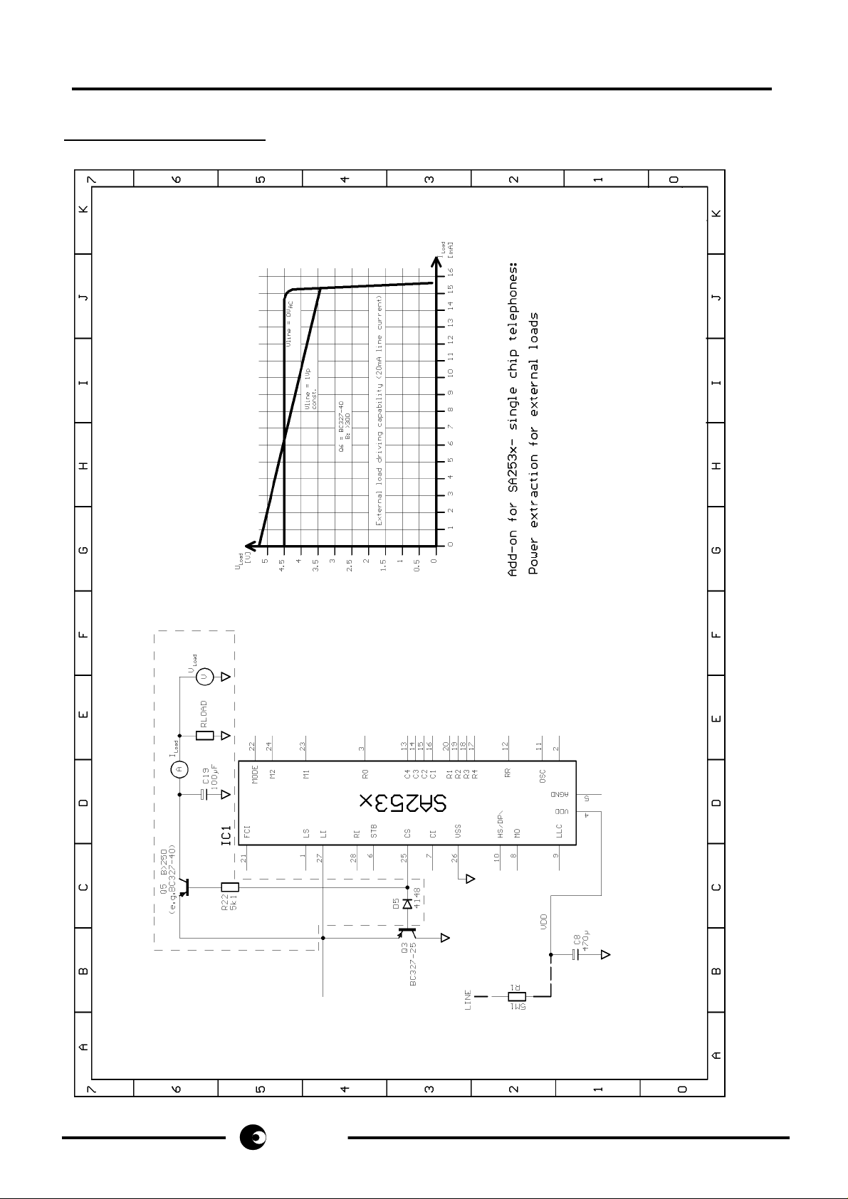
Note: all further component references apply to the schematic shown in pt.9 of this application note !
SAN3020 PDS038-SA2531/2-002 Rev. B 21-03-00
Page 2
SAN3020
When driving external loads by extracting power f rom the available line current, care m ust be taken not to affect
both DC and AC impedance. The extracted voltage should be independent from line current (assuming a line
current >20mA).
The application shown will shut off the exter nal load when going on-hook and power-up the load when going offhook.
The current driving capability depends on the available line current, higher line currents allow higher driving
currents. At minimum line current (20mA), the maximum load current is ≈15mA (see pt.6 for further details).
6 Hardware configuration
Only 4 external components , shown in the dotted area (1 general purpose PNP transistor:B
=250, 1 general
min
purpose diode , 1 resistor and 1 pol. capacitor) must be added to the standard SA253x application to get a high
efficiency power extraction for external loads with the features described in pt.5 above.
When updating an exis ting circuit, the connection from pin #25 (= CS, SA253x) to the shunt transis tor’s base (in
most applications = Q3) must be opened and a diode (D5) installed. All further components are simply added to the
circuit.
7 Circuit description
The shunt transistor (Q 3) is regulating the voltage at LI ( #27) to ≈ 4.5V. Consequently, the voltage at CS ( #25) is
V
- VBE. When adding D5, the voltage drop between LI and CS is Vc onst = 2x VBE. This constant voltage provides
LI
the base current of the power extraction transistor Q5 via R22.
The maxim um load c urrent also depends on the gain (B= I
have a B of ≥250 . Transistors with lower gain may also be used, but the maximum load current may be lower.
7.1 Minimum output voltage with high signals on line:
As shown in the diagram (pt. 9), the output voltage at high load curr ents will drop with high transmit or receive
signals on line, since the load is not supplied during the negative half- wave of the line s ignal. The diagram shows
the V
out/ILoad
In practical use, an AC signal of 2V
curves with no AC signal at line and with a constant AC line signal of 1V
is not present continuously, so the effective output voltage will be higher. It is
pp
also possible to buffer the voltage drop during line signal bursts by increasing the value of capacitor C19.
/ IB) of the transistor used. T he transistor used s hould
C
.
peak
However, the voltage decrease with high signal bursts on line should be taken into consideration when the load
voltage must not drop below a certain value.
8 Connecting loads at V
Small loads can also be connected at V
1. When on-hook, the load must only draw <1µA , because it is connected in parallel to the V
DD
directly, as long as the following rules are observed:
DD
-cap, which
DD
maintains mem ory data retention in on-hook state, charged by a 5MΩ resistor . A higher load current would
discharge this capacitor and erase the memory contents.
2. The load will also be supplied in ringing mode.
3. When off-hook, the load current can be <5mA, provided it does not exceed this current at any time.
2/4
same s
same s
same ssame s
Page 3
SAN3020
9 Application schematic
3/4
same s
same s
same ssame s
Page 4

SAN3020
10 Liability and Copyright Statement
Disclaimer:
Micro-Electronic Systems (Pty) Ltd ("SAMES”) and may not be copied or disclosed to a third party, in whole or in
part, without the express written consent of SAMES. T he information c ontained herein is current as of the date of
publication; however, delivery of this document shall not under any circum stances cr eate any implication that the
information contained herein is correct as of any time subsequent to such date. SAMES does not undertake to
inform any recipient of this docum ent of any changes in the information contained herein, and SAMES express ly
reserves the right to make changes in such inform ation, without notification,even if such changes would render
information contained herein inaccurate or incomplete. SAMES makes no representation or warranty that any
circuit designed by reference to the inform ation contained her ein, will func tion without error s and as intended by the
designer
.
The information contained in this document is confidential and proprietary to South African
South African Micro-Electronic Systems (Pty) Ltd
P O Box 15888, 33 Eland Street,
Lynn East, Koedoespoort Industrial Area,
0039 Pretoria,
Republic of South Africa, Republic of South Africa
Tel: 012 333-6021 Tel: Int +27 12 333-6021
Fax: 012 333-3158 Fax: Int +27 12 333-3158
W eb Site : http://www.sames.co.za
4/4
sames
sames
samessames
 Loading...