

Page 1

INTEGRATED CIRCUITS
DATA SH EET
SAA5252
Line twenty-one acquisition and
display (LITOD)
Product specification
Supersedes data of March 1995
File under Integrated Circuits, IC02
1996 Jul 18
Page 2

Philips Semiconductors Product specification
Line twenty-one acquisition and display (LITOD) SAA5252
FEATURES
• Complete ‘stand-alone’ Line 21 decoder in one package
• On-chip display RAM allowing full page Text mode
• Enhanced character display modes
• Full colour captions
• RGB interface for standard colour decoder ICs
• Automatic handling of Field 2 data
• Automatic selection of (1H, 1V), (2H, 1V) or (2H, 2V)
scan modes
• Onboard OSD facility using Character generator
• RGB inputs to support existing OSD ICs
2
C-bus or ‘stand-alone’ pin control
• I
• Automatic data-ready signal generation on data
acquisition
• Can decode signals recorded on standard VHS and
S-VHS tape.
GENERAL DESCRIPTION
The SAA5252 (LITOD) is a single-chip CMOS device,
which will acquire, decode and display Line 21 Closed
Captioning data from a 525-line composite video signal.
Operation as an On-Screen Display (OSD) device is also
possible. Normal and line progressive scan modes are
supported.
QUICK REFERENCE DATA
SYMBOL PARAMETER MIN. TYP. MAX. UNIT
V
DD
I
DD
V
syn
V
vid
T
amb
T
stg
supply voltage 4.5 5.0 5.5 V
supply current − 30 − mA
CVBS sync amplitude 0.1 0.3 0.6 V
CVBS video amplitude 0.7 1.0 1.4 V
operating ambient temperature −20 − +70 °C
storage temperature −55 − +125 °C
ORDERING INFORMATION
TYPE
NUMBER
NAME DESCRIPTION VERSION
PACKAGE
SAA5252P DIP24 plastic dual in-line package; 24 leads (600 mil) SOT101-1
SAA5252T SO24 plastic small outline package; 24 leads; body width 7.5 mm SOT137-1
1996 Jul 18 2
Page 3

Philips Semiconductors Product specification
Line twenty-one acquisition and display (LITOD) SAA5252
BLOCK DIAGRAM
V
V
SS DD
VH
i.c.
OSCIN
OSCGND
OSCOUT
BLACK
IREF
CVBS
19 18
21
22
OSCILLATOR
20
SAA5252
23
24
1
SYNC SEPARATOR
ACQUISITION TIMING
ADC
7 86
DISPLAY
TIMING
CHARACTER
ROM
CODE
INTERPRETER
AND
ADDRESSING
AND
DATA
DETECTOR
Fig.1 Block diagram.
CHARACTER
GENERATOR
ADDRESSING
PAGE
RAM
SERIAL/
PARALLEL
AND
PARITY
17
RGBREF
16
BLAN
15
R
ROUNDING
ITALICS
AND
RGB
MULTIPLEXOR
2
I C
INTERFACE
CONTROL
2
2
I C/DC
14
13
9
10
11
12
5
3
4
G
B
BLANIN
RIN
GIN
BIN
DR
SDA
SCL
MBB623 - 1
1996 Jul 18 3
Page 4

Philips Semiconductors Product specification
Line twenty-one acquisition and display (LITOD) SAA5252
PINNING
SYMBOL PIN DESCRIPTION
CVBS 1 composite video input; signal should be connected via a
100 nF capacitor
2
C/DC 2 input selects I2C or Direct Control
I
2
SDA 3 serial data port for I
direct control
SCL 4 serial clock input for I
direct control
DR 5 data-ready signal to microcontroller (active-LOW) or
mode select input for direct control
i.c. 6 internally connected; connect to V
operation
V 7 vertical reference input for display timing
H 8 horizontal reference input for display timing
BLANIN 9 video blanking input from external OSD device
RIN 10 RED video input from external OSD device
GIN 11 GREEN video input from external OSD device
BIN 12 BLUE video input from external OSD device
B 13 BLUE video output
G 14 GREEN video output
R 15 RED video output
BLAN 16 video blanking output
RGBREF 17 input voltage defining output HIGH level for RGB pins
for closed captioning output
V
DD
V
SS
18 +5 V supply
19 0 V ground
OSCOUT 20 oscillator output
OSCIN 21 oscillator input
OSCGND 22 oscillator ground
BLACK 23 video black level storage input; connected to V
100 nF capacitor
IREF 24 reference current input; connected to V
resistor
C-bus or mode select input for
2
C-bus or mode select input for
for normal
SS
SS
via 27 kΩ
SS
via
1
CVBS
2
I C/DC
BLANIN
SDA
SCL
DR
i.c.
RIN
GIN
BIN
2
3
4
5
6
V
H
SAA5252
7
8
9
10
11
12
MBB622 - 1
Fig.2 Pin configuration.
24
23
22
21
20
19
18
17
16
15
14
13
IREF
BLACK
OSCGND
OSCIN
OSCOUT
V
SS
V
DD
RGBREF
BLAN
R
G
B
1996 Jul 18 4
Page 5

Philips Semiconductors Product specification
Line twenty-one acquisition and display (LITOD) SAA5252
LIMITING VALUES
In accordance with the Absolute Maximum Rating System (IEC 134).
SYMBOL PARAMETER CONDITIONS MIN. MAX. UNIT
V
DD
V
Imax
V
Omax
V
dif
I
IOK
I
Omax
T
amb
T
stg
V
es
supply voltage (all supplies) −0.3 +6.5 V
maximum input voltage (any input) note 1 −0.3 VDD+ 0.5 V
maximum output voltage (any output) note 1 − VDD+ 0.5 V
difference between VSS and OSCGND −±0.25 V
DC input or output diode current −±20 mA
maximum output current (each output) −±10 mA
operating ambient temperature −20 +70 °C
storage temperature −55 +125 °C
electrostatic handling
human body model note 2 −2000 +2000 V
machine model note 3 −200 +200 V
Notes
1. This maximum value has an absolute maximum of 6.5 V independent of V
DD
.
2. The human body model ESD simulation is equivalent to discharging a 100 pF capacitor via a 1.5 kΩ resistor, which
produces a single discharge transient. Reference
to MIL-STD 883C method 3015.7)”
.
“Philips Semiconductors Test Method UZW-BO/FQ-A302 (similar
3. The machine model ESD simulation is equivalent to discharging a 200 pF capacitor via a resistor and series inductor
with effective dynamic values of 25 Ω and 2.5 µH, which produces a damped oscillating discharge. Reference
“Philips Semiconductors Test Method UZW-BO/FQ-B302 (similar to EIAJ IC-121 Test Method 20 condition C)”
.
Quality
This device will meet the requirements of the
in accordance with
“Quality Reference Handbook (order number 9397 750 00192)”
“Philips Semiconductors General Quality Specification UZW-BO/FQ-0601”
. This details the acceptance criteria
for all Q & R tests applied to the product.
1996 Jul 18 5
Page 6
Philips Semiconductors Product specification
Line twenty-one acquisition and display (LITOD) SAA5252
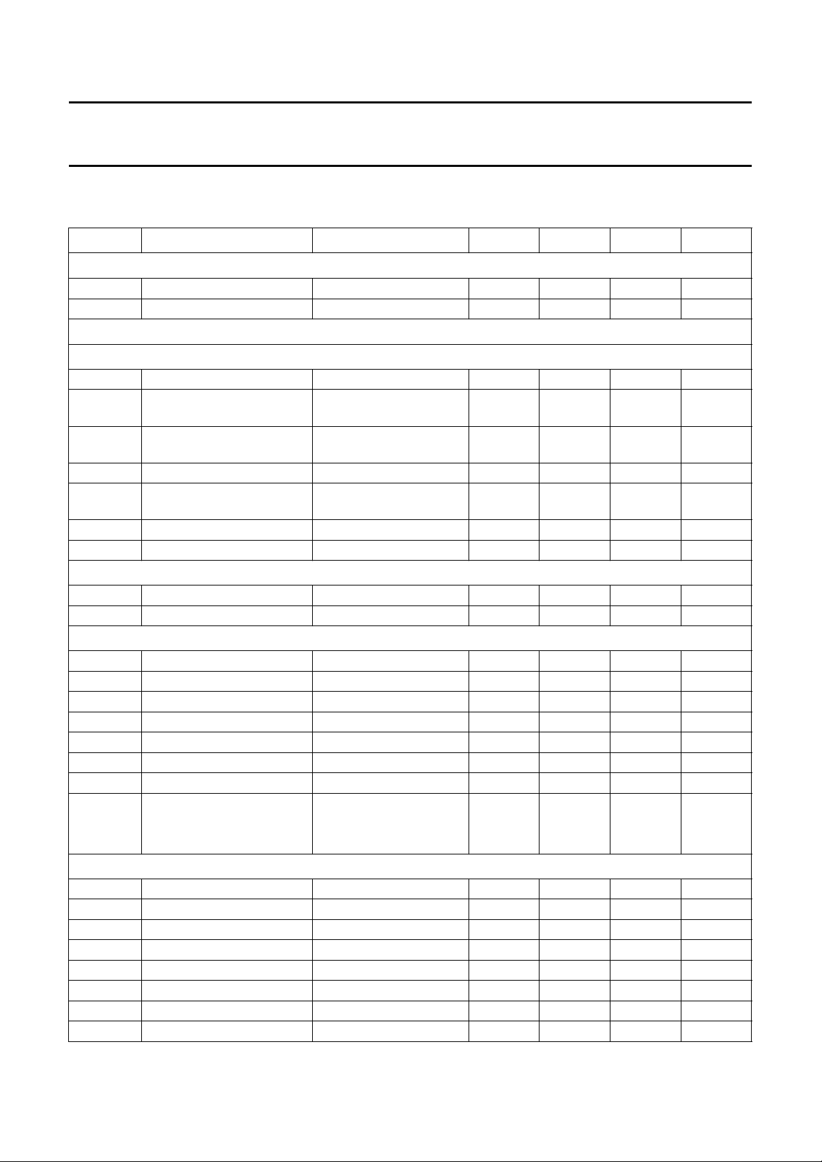
CHARACTERISTICS
V
= 5 to 5.5 V; VSS=0V; T
DD
SYMBOL PARAMETER CONDITIONS MIN. TYP. MAX. UNIT
Supplies
V
DD
I
DDtot
supply voltage 4.5 5.0 5.5 V
total supply current − 30 − mA
Inputs
= −20 to +70 °C; unless otherwise specified.
amb
CVBS (
V
V
V
Z
V
Z
C
PIN 1)
syn
vid(p-p)
dat
source
I
I
I
IREF (PIN 24)
R
24
V
24
H(PIN 8)
V
IL
V
IH
I
LI
I
Imax
C
I
t
r
t
f
t
W
PIN 7)
V(
V
IL
V
IH
I
LI
I
Imax
C
I
t
r
t
f
t
W
sync voltage amplitude 0.1 0.3 0.6 V
video voltage amplitude
0.7 1.0 1.4 V
(peak-to-peak value)
caption data voltage
0.25 0.35 0.49 V
amplitude
source impedance −−250 Ω
input switching voltage level
1.7 2.0 2.3 V
of sync separator
input impedance 2.5 5 − kΩ
input capacitance −−10 pF
resistor to ground − 27 − kΩ
voltage on pin 24 −
1
⁄2V
DD
− V
LOW level input voltage −0.3 − +0.8 V
HIGH level input voltage 2.0 − VDD+ 0.5 V
input leakage current VI=0toV
DD
−10 − +10 µA
maximum input current −1 − +1 mA
input capacitance −−10 pF
pulse rise time −−5µs
pulse fall time −−5µs
pulse width
scan mode 1H 1 12 63 µs
scan mode 2H 1 6 31 µs
LOW level input voltage −0.3 − +0.8 V
HIGH level input voltage 2.0 − VDD+ 0.5 V
input leakage current VI=0toV
DD
−10 − +10 µA
maximum input current −1 − +1 mA
input capacitance −−10 pF
pulse rise time −−5ns
pulse fall time −−5ns
pulse width 1 −−µs
1996 Jul 18 6
Page 7

Philips Semiconductors Product specification
Line twenty-one acquisition and display (LITOD) SAA5252
SYMBOL PARAMETER CONDITIONS MIN. TYP. MAX. UNIT
RGBREF (PIN, 17)
V
I
I
LI
input voltage −0.3 − V
input leakage current VI= 0 to V
R, G AND B(PINS 15, 14 AND 13); note 1
V
IL
V
IH
Z
I
LOW level input voltage −0.3 − 0.8 V
HIGH level input voltage 2.0 − VDD+ 0.5 V
input impedance 2.5 5.0 − kΩ
BLANIN (PIN 9)
V
IL
V
IH
I
LI
t
r
t
f
LOW level input voltage −0.3 − 0.8 V
HIGH level input voltage 2.0 − VDD+ 0.5 V
input leakage current VI =0toV
input rise time between 10% and 90% −−80 ns
input fall time between 90% and 10% −−80 ns
I2C/DC (PIN 2)
V
IL
V
IH
I
LI
LOW level input voltage 0 − 0.8 V
HIGH level input voltage 2.0 − V
input leakage current VI=0toV
SCL (PIN 4)
V
IL
V
IH
f
clk
t
r
t
f
I
LI
C
I
LOW level input voltage −0.3 − 1.5 V
HIGH level input voltage 3.0 − VDD+ 0.5 V
clock frequency 0 − 100 kHz
input rise time between 10% and 90% −−2µs
input fall time between 90% and 10% −−2µs
input leakage current VI=0 toV
input capacitance −−10 pF
Inputs/outputs
DD
DD
DD
DD
DD
−10 − +10 µA
−10 − +10 µA
DD
−10 − +10 µA
−10 − +10 µA
V
V
C
ERAMIC RESONATOR (PINS 20, 21 AND 22); see Fig.5
f
osc
oscillator frequency 11.82 12 12.18 MHz
C0 parallel capacitance − 5.35 − pF
C1 series capacitance − 37.4 − pF
L1 series inductance − 35.5 −µH
R1 series resistance − 625Ω
black
PIN 23)
storage capacitor to ground − 100 − nF
black level voltage for
1.8 2.15 2.5 V
BLACK (
C
V
black
nominal sync amplitude
I
LI
input leakage current VI=0toV
DD
−10 − +10 µA
1996 Jul 18 7
Page 8

Philips Semiconductors Product specification
Line twenty-one acquisition and display (LITOD) SAA5252
SYMBOL PARAMETER CONDITIONS MIN. TYP. MAX. UNIT
SDA (PIN 3; OPEN DRAIN)
V
IL
V
IH
I
LI
C
I
t
r
t
f
V
OL
t
f
C
L
DR (PIN 5; OPEN DRAIN)
V
IL
V
IH
I
LI
V
OL
t
f
C
L
Outputs
LOW level input voltage −0.3 − +1.5 V
HIGH level input voltage 3.0 − VDD+ 0.5 V
input leakage current VI=0toV
DD
−10 − +10 µA
input capacitance −−10 pF
input rise time between 10% and 90% −−2µs
input fall time between 90% and 10% −−2µs
LOW level output voltage IOL= 3 mA 0 − 0.5 V
output fall time between 3 V and 1 V −−200 ns
load capacitance −−400 pF
LOW level input voltage −0.3 − +1.5 V
HIGH level input voltage 3.0 − VDD+ 0.5 V
input leakage current VI=0toV
DD
−10 − +10 µA
LOW level output voltage IOL= 1.6 mA 0 − 0.4 V
output fall time between 4 V and 1 V with
−−50 ns
3.3 kΩ to 5 V
load capacitance −−100 pF
R, G
AND B(PINS 15, 14 AND 13; CAPTION MODE)
V
OL
V
OH
Z
O
C
L
t
r
t
f
LOW level output voltage IOL=+2mA 0 − 0.2 V
HIGH level output voltage IOH= −2mA V17− 0.3 V
output impedance −−200 Ω
load capacitance −−50 pF
output rise time between 10% and 90% −−10 ns
output fall time between 90% and 10% −−10 ns
BLAN (PIN 16)
V
V
C
t
r
t
f
t
skew
OL
OH
L
LOW level output voltage IOL=+2mA 0 − 0.4 V
HIGH level output voltage IOH= −2 mA 1.1 − 2.8 V
load capacitance −−50 pF
output rise time between 10% and 90% −−10 ns
output fall time between 90% and 10% −−10 ns
skew delay time between
display and R, G, B, BLAN
17
V17+ 0.4 V
−−10 ns
1996 Jul 18 8
Page 9

Philips Semiconductors Product specification
Line twenty-one acquisition and display (LITOD) SAA5252
SYMBOL PARAMETER CONDITIONS MIN. TYP. MAX. UNIT
I2C timing (see Fig.3)
t
LOW
t
HIGH
t
SU;DAT
t
HD;DAT
t
SU;STO
t
BUF
t
HD;STA
t
SU;STA
t
r
t
f
Note
1. These inputs are analog, VIL and VIH values are quoted as a guide for digital RGB users.
clock LOW time 4 −−µs
clock HIGH time 4 −−µs
data set-up time 250 −−ns
data hold time 170 −−ns
set-up time from clock
4 −−µs
HIGH-to-STOP
START set-up time
4 −−µs
following a STOP
START hold time 4 −−µs
START set-up time
4 −−µs
following clock
LOW-to-HIGH transition
output rise time between 10% and 90% −−10 ns
output fall time between 90% and 10% −−10 ns
handbook, full pagewidth
SDA
SCL
SDA
MBC764
t
BUF
t
LOW
t
HD;STA
t
t
SU;STA
Fig.3 I2C-bus timing diagram.
t
f
t
r
t
HD;DAT
HIGH
t
SU;DAT
t
SU;STO
1996 Jul 18 9
Page 10

Philips Semiconductors Product specification
Line twenty-one acquisition and display (LITOD) SAA5252
APPLICATION INFORMATION
handbook, full pagewidth
CVBS
5 V
3.3
microcontroller
kΩ
to
microcontroller
100 nF
C5
2
I C-bus
to
CVBS
2
I C/DC
SDA
SCL
DR
BLANIN
RIN
GIN
BIN
i.c.
V
H
1
2
3
4
5
6
SAA5252
7
8
9
10
11
12
24
23
22
21
20
19
18
17
16
15
14
13
IREF
BLACK
OSCGND
OSCIN
OSCOUT
V
SS
V
DD
RGBREF
BLAN
R
G
B
C4
27 kΩ
100 nF
C3
33 pF
33 pF
C7
100 nF
C2
C6
10 µF
5 V
5 V
12 MHz
MBB624 - 2
C3
10 nF
(1)
(1)
5 V
(1) Value dependent on application.
Fig.4 Application diagram.
C1
L1 R1
Fig.5 Ceramic resonator equivalent circuit.
1996 Jul 18 10
C0
MEA560
Page 11

Philips Semiconductors Product specification
Line twenty-one acquisition and display (LITOD) SAA5252
DISPLAY GENERATOR
General description
The displayed characters are defined on a 5-by-12 matrix
within a 7-by-13 window, allowing one blank pixel either
side of the character and a blank pixel row above. There
are a number of display options available controlled by
Register 1, or external pins in ‘stand-alone’ mode.
The three display modes are video, text and caption, the
device is powered up in the video mode.
The display generator reads the Pre-amble Address Code
(PAC) then the data associated with that row. Each
character is then rounded after which it can be italicized
and/or underlined, depending on the PAC or mid-row
codes, before being passed on to the output circuitry.
Figure 6 shows the character set.
Table 1 Register map (WRITE)
REGISTER D7 D6 D5 D4 D3 D2 D1 D0
00 DF
01 CLEAR CH 2/
02 −− − − ROW3 ROW2 ROW1 ROW0
03 −− − COL4 COL3 COL2 COL1 COL0
04 − OSD6 OSD5 OSD4 OSD3 OSD2 OSD1 OSD0
1/2 RGB, BLAN
+ve/−ve
1 NARROW/
H
+ve/−ve
WIDE
Display of external On-Screen Display (OSD) facilities
The R, G, B and BLAN outputs of the display have the
capability to be put in a 3-state mode allowing other OSD
devices to take control of the television R, G, B and BLAN
signals.
When the BLANIN is held HIGH then the R, G, B and
BLAN outputs from display are disabled and the R, G, B
and BLAN signals come directly from the RGBIN and
BLANIN inputs. This will allow On-Screen Display to be
placed on top of the captioning without any corruption,
leaving the captions intact when the On-Screen Display is
switched off (BLANIN goes LOW). In this form of operation
the RGBIN and RGBOUT pins can be considered
transparent; BLANIN goes through the normal output
buffer to BLAN.
V
+ve/−ve
ACQ OFF EN1 EN0 M1 M0
H3 H2 H1 H0
Table 2 Register map (READ)
REGISTER D7 D6 D5 D4 D3 D2 D1 D0
80 POR 0 0 0
81 PARITY
ERROR
82 PARITY
ERROR
1996 Jul 18 11
DATA
BIT 7
DATA
BIT 7
DATA
BIT 6
DATA
BIT 6
DATA
BIT 5
DATA
BIT 5
F1/F2 EDS PARITY
SHUTDOWN
DATA
BIT 4
DATA
BIT 4
DATA
BIT 3
DATA
BIT 3
DATA
BIT 2
DATA
BIT 2
DATA
READY
DATA
BIT 1
DATA
BIT 1
Page 12

Philips Semiconductors Product specification
Line twenty-one acquisition and display (LITOD) SAA5252
b
6
b3b2b1b
0 0 0 1
0 0 1 1
b
5
b
4
0
0
0
0
column
0 1234 567
r
o
w
00 0 0 0 white
white
1
underline
green
20 0 1 0
green
3
underline
40 1 0 0 blue
blue
50 1 0 1
underline
60 1 1 0 cyan
cyan
70 1 1 1
underline
81 0 0 0 red
0
0
1
0
0
1
1
0
1
11
1
0
011
0
1
1
0
1
signifies "flash on" command
signifies a transparent space
1 0 0 1
1 0 1 0
1 0 1 1
1 1 0 1
1 1 1 0
red
9
underline
A
yellow
yellow
B
underline
C1 1 0 0
magenta
magenta
D
underline
E
italics
italics
F1 1 1 1
underline
The ‘0’ and ‘zero’ use the same character, 4FH.
MBB625 - 2
Fig.6 Character set.
1996 Jul 18 12
Page 13

Philips Semiconductors Product specification
Line twenty-one acquisition and display (LITOD) SAA5252
I2C INTERFACE
Description of WRITE registers
The write subaddresses auto increment from 0 through to 4 at which point they stay until a new write subaddress is sent.
Registers are set to all logic 0 at power-up.
Table 3 Register 0 WRITE (Control Byte 1)
BIT DESCRIPTION
D0 to D3 H0 to H3 set the offset position from the start of the horizontal sync pulse, set to a nominal value on reset.
D4 Vertical sync pulse expected to be negative going logic 0 or positive-going logic 1.
D5 Horizontal sync pulse expected to be negative going logic 0 or positive-going logic 1.
D6 Video outputs will be positive going logic 0 or negative-going logic 1.
D7 Data field select. When set to logic 0 Field 1 is decoded, when set to logic 1 Field 2 is decoded.
Table 4 Register 1 WRITE (Control Byte 2)
BIT DESCRIPTION
D0, D1 Display mode selection bits. Table 8 shows the possible display modes.
D2, D3 Enhanced caption mode selection bits. Table 9 shows the possible enhanced caption modes.
D4 When set to logic 1 acquisition of caption data is inhibited to allow the display to be used for
On-Screen Display purposes.
D5 Acquisition window selection. When set to logic 0 only Line 21 is checked for caption data. When set to
logic 1, lines 19 to 23 of both fields are checked, allowing encrypted video signals to be handled.
D6 User channel selection.
D7 Clears the page memory when set HIGH. The page memory will be within two fields (30 ms).
Table 5 Register 2 WRITE (On-Screen Display data row address)
BIT DESCRIPTION
D0 to D3 Row 0 to 3 sets the row address for On-Screen Display. This stored value will be incremented by overflow
increments of Register 3.
Table 6 Register 3 WRITE (On-Screen Display data column address)
BIT DESCRIPTION
D0 to D4 Columns 0 to 4 sets the column address for On-Screen Display. This stored value will be incremented by
writes to Register 4.
Table 7 Register 4 WRITE (On-Screen Display data)
BIT DESCRIPTION
D0 to D6 OSD0 to OSD6, On-Screen Display data bits writing to this register causes Register 3 to increment its
stored value.
1996 Jul 18 13
Page 14

Philips Semiconductors Product specification
Line twenty-one acquisition and display (LITOD) SAA5252
Table 8 Display modes
DISPLAY MODE OPTIONS M1 M0
Video only 0 0
Text mode 0 1
Normal caption mode 1 0
Enhanced caption mode 1 1
Table 9 Enhanced caption modes
ENHANCED CAPTION MODES EN1 EN0
Enhanced caption modes EN1 EN0
Shadowed character/Video background 0 0
Shadowed character/Mesh background 0 1
Normal character/Video background 1 0
Normal character/Mesh background 1 1
Description of READ registers
The read subaddresses auto increment from 80H through to 82H at which point they stay until a new read subaddress
is sent.
All the bits in Table 10 are reset to logic 0 after the register is read.
Table 10 Register 80H READ (status)
BIT DESCRIPTION
D0 Data ready (new data has been acquired).
D1 Parity error shut-down, goes HIGH when SAA5252 has a parity shut-down condition.
D2 Indicates the following bytes are extended data service bytes.
D3 Indicates Field 1 or Field 2 data bytes.
2
D7 Indicates Power-On Reset (POR) has occurred, all I
Table 11 Register 81H READ (first data byte)
BIT DESCRIPTION
D0 to D6 Data Bit 1 to Data Bit 7 (see note 1).
D7 Parity error flag bit. Bit goes HIGH when a parity error has occurred.
Note
1. In the Line 21, specification data bits are numbered D1 to D8.
C-bus write registers have been reset to logic 0.
Table 12 Register 82H READ (second data byte)
BIT DESCRIPTION
D0 to D6 Data Bit 1 to Data Bit 7 (see note 1).
D7 Parity error flag bit. Bit goes HIGH when a parity error has occurred.
Note
1. In the Line 21, specification data bits are numbered D1 to D8.
1996 Jul 18 14
Page 15

Philips Semiconductors Product specification
Line twenty-one acquisition and display (LITOD) SAA5252
Interface to microcontroller using I2C-bus
The interface to the microcontroller is via the two-wire
serial I2C-bus, and optionally by a Data-Ready signal
(DR). On power up the microcontroller initializes the
device by an I2C-bus WRITE to Registers 0
(Control Byte 1). The I2C-bus subaddress is then auto
incremented to point to Register 1 (Control Byte 2). These
two registers configure the device to the users
requirements.
If the device is to be used for data acquisition only, then
there are three methods by which the microcontroller can
be informed of the arrival of valid Line 21 data:
• It can poll the DR pin, if the function has been enabled,
and wait for it to go LOW.
• It can use the negative edge of the DR signal to cause
an interrupt.
• It can poll the Data Ready bit (bit D0 of the status byte,
I2C-bus READ Register 0).
When valid data is detected, the microcontroller must
initiate an I2C-bus READ of Registers 80H, 81H and 82H.
The first and second data bytes from the most recently
received Line 21 are in Register 81H and Register 82H
respectively.
The DR pin, and the Data Ready bit (Status bit D0) will be
cleared after any register has been read. POR is reset
after Register 80H has been read.
‘STAND-ALONE’ (NON I2C-BUS) OPERATION
To set the SAA5252 for ‘stand-alone’ operation pin 2
(I2C/DC) is tied LOW. This will change the operation of the
SCL, SDA and DR pins to mode select inputs which will
select as shown in Table 13.
In the caption mode the SAA5252 operates in the basic
Normal character/Black background mode. This complies
with the FCC ruling. In the Enhanced caption mode the
set-up will be Shadowed character/Video background.
SDA and SCL in the ‘stand-alone’ operation act as bits M0
and M1 in Table 8.
Table 13 Stand-alone modes
DR SCL SDA
0 0 0 video mode Channel 1
0 0 1 text mode Channel 1
0 1 0 normal captions Channel 1
0 1 1 enhanced captions Channel 1
1 0 0 video mode Channel 2
1 0 1 text mode Channel 2
1 1 0 normal captions Channel 2
1 1 1 enhanced captions Channel 2
MODE OF
OPERATION
CHANNEL
RECEPTION
1996 Jul 18 15
Page 16
Philips Semiconductors Product specification
Line twenty-one acquisition and display (LITOD) SAA5252
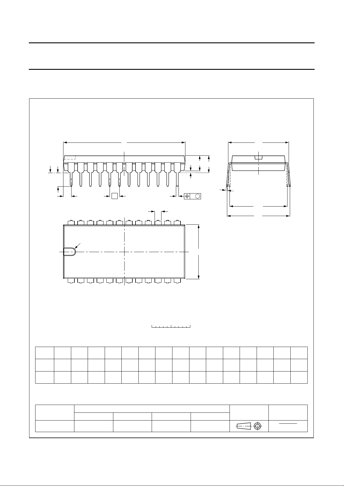
PACKAGE OUTLINES
DIP24: plastic dual in-line package; 24 leads (600 mil)
D
seating plane
L
Z
24
pin 1 index
e
b
SOT101-1
M
E
A
2
A
A
1
w M
b
1
13
E
c
(e )
1
M
H
1
0 5 10 mm
scale
DIMENSIONS (inch dimensions are derived from the original mm dimensions)
A
A
A
UNIT
inches
Note
1. Plastic or metal protrusions of 0.25 mm maximum per side are not included.
max.
mm
OUTLINE
VERSION
SOT101-1
1 2
min.
max.
1.7
1.3
0.066
0.051
IEC JEDEC EIAJ
051G02 MO-015AD
b
b
1
0.53
0.38
0.021
0.015
0.32
0.23
0.013
0.009
REFERENCES
cD E e M
32.0
31.4
1.26
1.24
1996 Jul 18 16
12
14.1
13.7
0.56
0.54
(1)(1)
e
L
3.9
3.4
EUROPEAN
PROJECTION
M
E
15.80
15.24
0.62
0.60
17.15
15.90
0.68
0.63
1
0.15
0.13
H
ISSUE DATE
w
0.252.54 15.24
0.010.10 0.60
92-11-17
95-01-23
Z
max.
2.25.1 0.51 4.0
0.0870.20 0.020 0.16
(1)
Page 17

Philips Semiconductors Product specification
Line twenty-one acquisition and display (LITOD) SAA5252
SO24: plastic small outline package; 24 leads; body width 7.5 mm
D
c
y
Z
24
pin 1 index
1
e
13
12
w M
b
p
SOT137-1
E
H
E
Q
A
2
A
1
L
p
L
detail X
(A )
A
X
v M
A
A
3
θ
0 5 10 mm
scale
DIMENSIONS (inch dimensions are derived from the original mm dimensions)
mm
OUTLINE
VERSION
SOT137-1
A
max.
2.65
0.10
A1A2A
0.30
2.45
0.10
2.25
0.012
0.096
0.004
0.089
IEC JEDEC EIAJ
075E05 MS-013AD
0.25
0.01
b
3
p
0.49
0.32
0.36
0.23
0.019
0.013
0.014
0.009
UNIT
inches
Note
1. Plastic or metal protrusions of 0.15 mm maximum per side are not included.
(1)E(1) (1)
cD
15.6
7.6
7.4
0.30
0.29
1.27
0.050
15.2
0.61
0.60
REFERENCES
1996 Jul 18 17
eHELLpQ
10.65
10.00
0.42
0.39
1.4
0.055
1.1
0.4
0.043
0.016
1.1
1.0
0.043
0.039
PROJECTION
0.25
0.25 0.1
0.01
0.01
EUROPEAN
ywv θ
Z
0.9
0.4
8
0.004
ISSUE DATE
0.035
0.016
92-11-17
95-01-24
0
o
o
Page 18

Philips Semiconductors Product specification
Line twenty-one acquisition and display (LITOD) SAA5252
SOLDERING
Introduction
There is no soldering method that is ideal for all IC
packages. Wave soldering is often preferred when
through-hole and surface mounted components are mixed
on one printed-circuit board. However, wave soldering is
not always suitable for surface mounted ICs, or for
printed-circuits with high population densities. In these
situations reflow soldering is often used.
This text gives a very brief insight to a complex technology.
A more in-depth account of soldering ICs can be found in
our
“IC Package Databook”
(order code 9398 652 90011).
DIP
OLDERING BY DIPPING OR BY WA VE
S
The maximum permissible temperature of the solder is
260 °C; solder at this temperature must not be in contact
with the joint for more than 5 seconds. The total contact
time of successive solder waves must not exceed
5 seconds.
The device may be mounted up to the seating plane, but
the temperature of the plastic body must not exceed the
specified maximum storage temperature (T
stg max
). If the
printed-circuit board has been pre-heated, forced cooling
may be necessary immediately after soldering to keep the
temperature within the permissible limit.
EPAIRING SOLDERED JOINTS
R
Apply a low voltage soldering iron (less than 24 V) to the
lead(s) of the package, below the seating plane or not
more than 2 mm above it. If the temperature of the
soldering iron bit is less than 300 °C it may remain in
contact for up to 10 seconds. If the bit temperature is
between 300 and 400 °C, contact may be up to 5 seconds.
SO
REFLOW SOLDERING
Reflow soldering techniques are suitable for all SO
packages.
Several techniques exist for reflowing; for example,
thermal conduction by heated belt. Dwell times vary
between 50 and 300 seconds depending on heating
method. Typical reflow temperatures range from
215 to 250 °C.
Preheating is necessary to dry the paste and evaporate
the binding agent. Preheating duration: 45 minutes at
45 °C.
AVE SOLDERING
W
Wave soldering techniques can be used for all SO
packages if the following conditions are observed:
• A double-wave (a turbulent wave with high upward
pressure followed by a smooth laminar wave) soldering
technique should be used.
• The longitudinal axis of the package footprint must be
parallel to the solder flow.
• The package footprint must incorporate solder thieves at
the downstream end.
During placement and before soldering, the package must
be fixed with a droplet of adhesive. The adhesive can be
applied by screen printing, pin transfer or syringe
dispensing. The package can be soldered after the
adhesive is cured.
Maximum permissible solder temperature is 260 °C, and
maximum duration of package immersion in solder is
10 seconds, if cooled to less than 150 °C within
6 seconds. Typical dwell time is 4 seconds at 250 °C.
A mildly-activated flux will eliminate the need for removal
of corrosive residues in most applications.
EPAIRING SOLDERED JOINTS
R
Fix the component by first soldering two diagonally-
opposite end leads. Use only a low voltage soldering iron
(less than 24 V) applied to the flat part of the lead. Contact
time must be limited to 10 seconds at up to 300 °C. When
using a dedicated tool, all other leads can be soldered in
one operation within 2 to 5 seconds between
270 and 320 °C.
Reflow soldering requires solder paste (a suspension of
fine solder particles, flux and binding agent) to be applied
to the printed-circuit board by screen printing, stencilling or
pressure-syringe dispensing before package placement.
1996 Jul 18 18
Page 19

Philips Semiconductors Product specification
Line twenty-one acquisition and display (LITOD) SAA5252
DEFINITIONS
Data sheet status
Objective specification This data sheet contains target or goal specifications for product development.
Preliminary specification This data sheet contains preliminary data; supplementary data may be published later.
Product specification This data sheet contains final product specifications.
Limiting values
Limiting values given are in accordance with the Absolute Maximum Rating System (IEC 134). Stress above one or
more of the limiting values may cause permanent damage to the device. These are stress ratings only and operation
of the device at these or at any other conditions above those given in the Characteristics sections of the specification
is not implied. Exposure to limiting values for extended periods may affect device reliability.
Application information
Where application information is given, it is advisory and does not form part of the specification.
LIFE SUPPORT APPLICATIONS
These products are not designed for use in life support appliances, devices, or systems where malfunction of these
products can reasonably be expected to result in personal injury. Philips customers using or selling these products for
use in such applications do so at their own risk and agree to fully indemnify Philips for any damages resulting from such
improper use or sale.
2
PURCHASE OF PHILIPS I
C COMPONENTS
2
Purchase of Philips I
components in the I2C system provided the system conforms to the I2C specification defined by
Philips. This specification can be ordered using the code 9398 393 40011.
C components conveys a license under the Philips’ I2C patent to use the
1996 Jul 18 19
Page 20

Philips Semiconductors – a worldwide company
Argentina: see South America
Australia: 34 Waterloo Road, NORTH RYDE, NSW 2113,
Tel. +61 2 9805 4455, Fax. +61 2 9805 4466
Austria: Computerstr. 6, A-1101 WIEN, P.O. Box 213,
Tel. +43 1 60 101, Fax. +43 1 60 101 1210
Belarus: Hotel Minsk Business Center, Bld. 3, r. 1211, Volodarski Str. 6,
220050 MINSK, Tel. +375 172 200 733, Fax. +375 172 200 773
Belgium: see The Netherlands
Brazil: see South America
Bulgaria: Philips Bulgaria Ltd., Energoproject, 15thfloor,
51 James Bourchier Blvd., 1407 SOFIA,
Tel. +359 2 689 211, Fax. +359 2 689 102
Canada: PHILIPS SEMICONDUCTORS/COMPONENTS,
Tel. +1 800 234 7381, Fax. +1 708 296 8556
China/Hong Kong: 501 Hong Kong Industrial Technology Centre,
72 Tat Chee Avenue, Kowloon Tong, HONG KONG,
Tel. +852 2319 7888, Fax. +852 2319 7700
Colombia: see South America
Czech Republic: see Austria
Denmark: Prags Boulevard 80, PB 1919, DK-2300 COPENHAGEN S,
Tel. +45 32 88 2636, Fax. +45 31 57 1949
Finland: Sinikalliontie 3, FIN-02630 ESPOO,
Tel. +358 615 800, Fax. +358 615 80920
France: 4 Rue du Port-aux-Vins, BP317, 92156 SURESNES Cedex,
Tel. +33 1 40 99 6161, Fax. +33 1 40 99 6427
Germany: Hammerbrookstraße 69, D-20097 HAMBURG,
Tel. +49 40 23 52 60, Fax. +49 40 23 536 300
Greece: No. 15, 25th March Street, GR 17778 TAVROS,
Tel. +30 1 4894 339/911, Fax. +30 1 4814 240
Hungary: see Austria
India: Philips INDIA Ltd, Shivsagar Estate, A Block, Dr. Annie Besant Rd.
Worli, MUMBAI 400 018, Tel. +91 22 4938 541, Fax. +91 22 4938 722
Indonesia: see Singapore
Ireland: Newstead, Clonskeagh, DUBLIN 14,
Tel. +353 1 7640 000, Fax. +353 1 7640 200
Israel: RAPAC Electronics, 7 Kehilat Saloniki St, TEL AVIV 61180,
Tel. +972 3 645 0444, Fax. +972 3 648 1007
Italy: PHILIPS SEMICONDUCTORS, Piazza IV Novembre 3,
20124 MILANO, Tel. +39 2 6752 2531, Fax. +39 2 6752 2557
Japan: Philips Bldg 13-37, Kohnan 2-chome, Minato-ku, TOKYO 108,
Tel. +81 3 3740 5130, Fax. +81 3 3740 5077
Korea: Philips House, 260-199 Itaewon-dong, Yongsan-ku, SEOUL,
Tel. +82 2 709 1412, Fax. +82 2 709 1415
Malaysia: No. 76 Jalan Universiti, 46200 PETALING JAYA, SELANGOR,
Tel. +60 3 750 5214, Fax. +60 3 757 4880
Mexico: 5900 Gateway East, Suite 200, EL PASO, TEXAS 79905,
Tel. +1 800 234 7381, Fax. +1 708 296 8556
Middle East: see Italy
Netherlands: Postbus 90050, 5600 PB EINDHOVEN, Bldg. VB,
Tel. +31 40 27 83749, Fax. +31 40 27 88399
New Zealand: 2 Wagener Place, C.P.O. Box 1041, AUCKLAND,
Tel. +64 9 849 4160, Fax. +64 9 849 7811
Norway: Box 1, Manglerud 0612, OSLO,
Tel. +47 22 74 8000, Fax. +47 22 74 8341
Philippines: Philips Semiconductors Philippines Inc.,
106 Valero St. Salcedo Village, P.O. Box 2108 MCC, MAKATI,
Metro MANILA, Tel. +63 2 816 6380, Fax. +63 2 817 3474
Poland: Ul. Lukiska 10, PL 04-123 WARSZAWA,
Tel. +48 22 612 2831, Fax. +48 22 612 2327
Portugal: see Spain
Romania: see Italy
Russia: Philips Russia, Ul. Usatcheva 35A, 119048 MOSCOW,
Tel. +7 095 926 5361, Fax. +7 095 564 8323
Singapore: Lorong 1, Toa Payoh, SINGAPORE 1231,
Tel. +65 350 2538, Fax. +65 251 6500
Slovakia: see Austria
Slovenia: see Italy
South Africa: S.A. PHILIPS Pty Ltd., 195-215 Main Road Martindale,
2092 JOHANNESBURG, P.O. Box 7430 Johannesburg 2000,
Tel. +27 11 470 5911, Fax. +27 11 470 5494
South America: Rua do Rocio 220, 5th floor, Suite 51,
04552-903 São Paulo, SÃO PAULO - SP, Brazil,
Tel. +55 11 821 2333, Fax. +55 11 829 1849
Spain: Balmes 22, 08007 BARCELONA,
Tel. +34 3 301 6312, Fax. +34 3 301 4107
Sweden: Kottbygatan 7, Akalla, S-16485 STOCKHOLM,
Tel. +46 8 632 2000, Fax. +46 8 632 2745
Switzerland: Allmendstrasse 140, CH-8027 ZÜRICH,
Tel. +41 1 488 2686, Fax. +41 1 481 7730
Taiwan: PHILIPS TAIWAN Ltd., 23-30F, 66,
Chung Hsiao West Road, Sec. 1, P.O. Box 22978,
TAIPEI 100, Tel. +886 2 382 4443, Fax. +886 2 382 4444
Thailand: PHILIPS ELECTRONICS (THAILAND) Ltd.,
209/2 Sanpavuth-Bangna Road Prakanong, BANGKOK 10260,
Tel. +66 2 745 4090, Fax. +66 2 398 0793
Turkey: Talatpasa Cad. No. 5, 80640 GÜLTEPE/ISTANBUL,
Tel. +90 212 279 2770, Fax. +90 212 282 6707
Ukraine: PHILIPS UKRAINE, 2A Akademika Koroleva str., Office 165,
252148 KIEV, Tel. +380 44 476 0297/1642, Fax. +380 44 476 6991
United Kingdom: Philips Semiconductors Ltd., 276 Bath Road, Hayes,
MIDDLESEX UB3 5BX, Tel. +44 181 730 5000, Fax. +44 181 754 8421
United States: 811 East Arques Avenue, SUNNYVALE, CA 94088-3409,
Tel. +1 800 234 7381, Fax. +1 708 296 8556
Uruguay: see South America
Vietnam: see Singapore
Yugoslavia: PHILIPS, Trg N. Pasica 5/v, 11000 BEOGRAD,
Tel. +381 11 825 344, Fax.+381 11 635 777
For all other countries apply to: Philips Semiconductors, Marketing & Sales Communications,
Building BE-p, P.O. Box 218, 5600 MD EINDHOVEN, The Netherlands, Fax. +31 40 27 24825
© Philips Electronics N.V. 1996 SCA50
All rights are reserved. Reproduction in whole or in part is prohibited without the prior written consent of the copyright owner.
The information presented in this document does not form part of any quotation or contract, is believed to be accurate and reliable and may be changed
without notice. No liability will be accepted by the publisher for any consequence of its use. Publication thereof does not convey nor imply any license
under patent- or other industrial or intellectual property rights.
Printed in The Netherlands 537021/01/04/pp20 Date of release: 1996 Jul 18 Document order number: 9397 750 00975
Internet: http://www.semiconductors.philips.com/ps/
(1) SAA5252_4 June 26, 1996 11:51 am
 Loading...