

Page 1

INTEGRATED CIRCUITS
DATA SH EET
SAA5288
TV microcontroller with full screen
On Screen Display (OSD)
Preliminary specification
File under Integrated Circuits, IC02
1997 Jun 24
Page 2

Philips Semiconductors Preliminary specification
TV microcontroller with full screen
On Screen Display (OSD)
CONTENTS
1 FEATURES
1.1 General
1.2 Microcontroller
1.3 Display
2 GENERAL DESCRIPTION
3 QUICK REFERENCE DATA
4 ORDERING INFORMATION
5 BLOCK DIAGRAM
6 PINNING INFORMATION
6.1 Pinning
6.2 Pin description
7 FUNCTIONAL DESCRIPTION
7.1 Microcontroller
7.2 80C51 features not supported
7.2.1 Interrupt priority
7.2.2 Off-chip memory
7.2.3 Idle and Power-down modes
7.2.4 UART function
7.3 Additional features
7.3.1 Interrupts
7.3.2 Bit Level I2C-bus Interface
7.3.3 Byte Level I2C-bus Interface
7.3.4 LED support
7.3.5 6-bit PWM DACs
7.3.6 14-bit PWM DAC
7.3.7 Software ADC
7.4 Microcontroller Interfacing
7.4.1 Special Function Register map
7.4.2 Special Function Registers bit description
7.5 The display
7.5.1 Introduction
7.5.2 Character matrix
7.5.3 Page attributes
7.5.4 East/west selection
7.5.5 National option characters
7.6 The twist attribute
7.6.1 On screen display symbols
7.6.2 Language group identification
7.6.3 525-line operation
7.6.4 Control characters
7.6.5 Display modes
7.7 On Screen Display boxes
7.8 Screen colour
SAA5288
7.9 Cursor
7.10 Other display features
7.11 Display timing
7.12 Horizontal timing
7.13 Vertical timing
7.14 Display position
7.15 Clock generator
8 CHARACTER SETS
8.1 Pan-European
8.2 Russian
8.3 Greek/Turkish
8.4 Arabic/English/French
8.5 Thai
8.6 Arabic/Hebrew
9 LIMITING VALUES
10 CHARACTERISTICS
11 CHARACTERISTICS FOR THE I2C-BUS
INTERFACE
12 QUALITY SPECIFICATIONS
13 APPLICATION INFORMATION
14 EMC GUIDELINES
15 PACKAGE OUTLINE
16 SOLDERING
16.1 Introduction
16.2 Soldering by dipping or by wave
16.3 Repairing soldered joints
17 DEFINITIONS
18 LIFE SUPPORT APPLICATIONS
19 PURCHASE OF PHILIPS I2C COMPONENTS
1997 Jun 24 2
Page 3

Philips Semiconductors Preliminary specification
TV microcontroller with full screen
On Screen Display (OSD)
1 FEATURES
1.1 General
• On-chip TV control tuning
• Hardware and software compatible with SAA5290,
SAA5291 and SAA5296
• Single +5 V power supply
• RGB interface to standard decoder ICs, push-pull output
drive
• SDIP52 package
• Single crystal oscillator for display and microcontroller.
1.2 Microcontroller
• 80C51 microcontroller core
• 16 kbyte mask programmed ROM
• 256 bytes of microcontroller RAM
• Eight 6-bit Pulse Width Modulator (PWM) outputs for
control of TV analog signals
• One 14-bit PWM for Voltage Synthesis tuner control
• Four 8-bit Analog-to-Digital Converters (ADCs)
• 2 high current open-drain outputs for directly driving
LED’s etc.
• Switchable bit or byte-oriented I
1.3 Display
• Single page (1024 × 8) on-board On Screen Display
(OSD) memory
• Double size width and height capability for OSD
• Enhanced display features including meshing,
shadowing and additional display attributes
2
C-bus interface.
SAA5288
• 260 characters in mask programmed ROM
• Display clock derived internally to reduce peripheral
components to a minimum
• Automatic FRAME output control with manual override
• Standby mode for display hardware
• 525-line and 625-line display
• 12 × 10 character matrix
• Stable Display via slave synchronization to Horizontal
Sync and Vertical Sync.
2 GENERAL DESCRIPTION
The SAA5288 is a microcontroller for use in televisions
with an OSD generator compatible with the Economy
Teletext/TV microcontroller family (SAA5290, SAA5291,
SAA5296 etc.). TV control facilities are provided by an
on-chip industry standard 80C51 microcontroller and a
1 kbyte DRAM is included for OSD memory.
Hardware and software compatibility with the Economy
Teletext/TV microcontroller family minimizes the changes
required to develop a TV control function for areas where
teletext is not broadcast.
The device cannot acquire Teletext but is based on a
Teletext device. Therefore, throughout this document
references are made to Teletext especially when
describing the Display/OSD section. The Display/OSD
section is fully compatible with a Teletext display and has
all the features associated with Teletext (i.e. double
height/width, flash, teletext boxes, graphics, etc.).
The Display section is described with reference to Teletext
to allow software compatibility with the Economy
Teletext/TV microcontroller family.
3 QUICK REFERENCE DATA
SYMBOL PARAMETER MIN. TYP. MAX. UNIT
V
DD
I
DDM
I
DDA
I
DDT
f
xtal
T
amb
supply voltage (all supplies) 4.5 5.0 5.5 V
microcontroller supply current − 15 30 mA
analogue supply current − 815mA
display supply current − 15 30 mA
crystal frequency − 12 − MHz
operating ambient temperature −20 − +70
1997 Jun 24 3
°
C
Page 4
Philips Semiconductors Preliminary specification
TV microcontroller with full screen
SAA5288
On Screen Display (OSD)
4 ORDERING INFORMATION
TYPE NUMBER
NAME DESCRIPTION VERSION
SAA5288PS/nnn SDIP52 plastic shrink dual in-line package; 52 leads (600 mil) SOT247-1
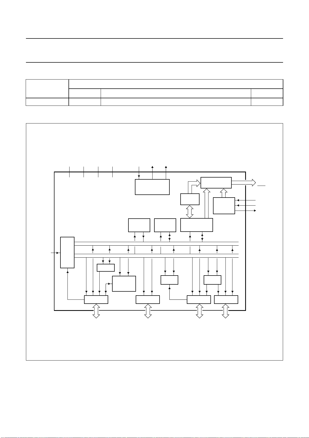
5 BLOCK DIAGRAM
handbook, full pagewidth
V
DDA
V
DDD
DDMVSSD
XTALINV
XTALOUT OSCGND
OSCILLATOR
PACKAGE
PAGE
RAM
DISPLAY
DISPLAY
TIMING
R, G, B,
VDS,
COR
VSYNC
HSYNC
FRAME
RESET
8051
CPU
data
address
interrupt
PORT 1
I2C-BUS
TIMER/
COUNTER
16 KBYTE
ROM
256 BYTE
RAM
ADC
PORT 0
Fig.1 Block diagram.
TEXT
INTERFACE
PORT 3
P3.0 to P3.7P0.0 to P0.7P1.0 to P1.7
PWM
PORT 2
MGL121
P2.0 to P2.7
1997 Jun 24 4
Page 5

Philips Semiconductors Preliminary specification
TV microcontroller with full screen
On Screen Display (OSD)
6 PINNING INFORMATION
6.1 Pinning
handbook, halfpage
P2.0/TPWM
P2.1/PWM0
P2.2/PWM1
P2.3/PWM2
P2.4/PWM3
P2.5/PWM4
P2.6/PWM5
P2.7/PWM6
P3.0/ADC0
P3.1/ADC1
P3.2/ADC2
P3.3/ADC3
V
SSD
P0.0
P0.1
P0.2
P0.3
P0.4
P0.5
P0.6
P0.7
V
SSD
IREF
i.c.
i.c.
i.c.
1
2
3
4
5
6
7
8
9
10
11
12
13
14
15
16
17
18
19
20
21
22
23
24
25
26
SAA5288
MGL114
52
P1.5
51
P1.4
50
P1.7/SDA
49
P1.6/SCL
48
P1.3/T1
47
P1.2/INT0
46
P1.1/T0
45
P1.0/INT
44
V
DDM
43
RESET
42
XTALOUT
41
XTALIN
40
OSCGND
39
V
DDD
38
V
DDA
37
VSYNC
36
HSYNC
35
VDS
34
R
33
G
32
B
31
RGBREF
30
P3.4/PWM7
29
COR
28
V
SSD
27
FRAME
SAA5288
Fig.2 Pin configuration.
1997 Jun 24 5
Page 6

Philips Semiconductors Preliminary specification
TV microcontroller with full screen
On Screen Display (OSD)
6.2 Pin description
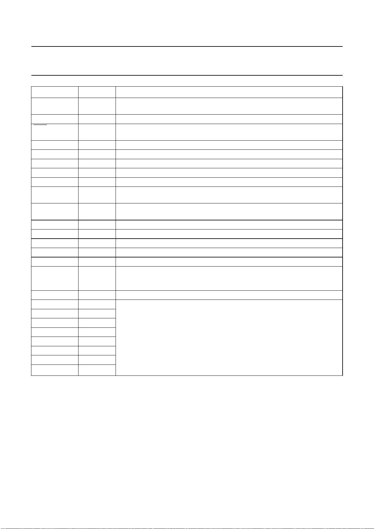
Table 1 SDIP52 package
SYMBOL PIN DESCRIPTION
P2.0/TPWM 1 Port 2. 8-bit open-drain bidirectional port with alternative functions.
P2.1/PWM0 2
P2.2/PWM1 3
P2.3/PWM2 4
P2.4/PWM3 5
P2.5/PWM4 6
P2.6/PWM5 7
P2.7/PWM6 8
P3.0/ADC0 9 Port 3. 8-bit open-drain bidirectional port with alternative functions.
P3.1/ADC1 10
P3.2/ADC2 11
P3.3/ADC3 12
P3.4/PWM7 30
V
SSD
P0.0 14 Port 0. 8-bit open-drain bidirectional port.
P0.1 15
P0.2 16
P0.3 17
P0.4 18
P0.5 19
P0.6 20
P0.7 21
V
SSD
i.c. 23 Internally connected; this pin should be connected to digital ground.
i.c. 24 Internally connected; this pin should be connected to digital ground.
i.c. 25 Internally connected; this pin should be connected to digital ground.
IREF 26 Reference current input for analog current generator, connected to V
13 Digital ground
22 Digital ground.
P2.0/TPWM is the output for the 14-bit high precision PWM.
P2.1/PWM0 to P2.7/PWM6 are the outputs for the 6-bit PWMs 0 to 6.
P3.0/ADC0 to P3.3/ADC3 are the inputs for the software ADC facility.
P3.4/PWM7 is the output for the 6-bit PWM7.
P0.5 and P0.6 have 10 mA current sinking capability for direct drive of LEDs.
resistor.
SAA5288
via a 27 kΩ
SSA
1997 Jun 24 6
Page 7
Philips Semiconductors Preliminary specification
TV microcontroller with full screen
SAA5288
On Screen Display (OSD)
SYMBOL PIN DESCRIPTION
FRAME 27 De-interlace output synchronised with the VSYNC pulse to produce a non-interlaced
display by adjustment of the vertical deflection circuits.
V
SSD
COR 29 Open-drain, active LOW output which allows selective contrast reduction of the TV
RGBREF 31 DC input voltage to define the output HIGH level on the RGB pins.
B 32 Pixel rate output of the BLUE colour information.
G 33 Pixel rate output of the GREEN colour information.
R 34 Pixel rate output of the RED colour information.
VDS 35 Video/data switch push-pull output for dot rate fast blanking.
HSYNC 36 Schmitt trigger input for a TTL level version of the horizontal sync pulse; the polarity
VSYNC 37 Schmitt trigger input for a TTL level version of the vertical sync pulse; the polarity of
V
DDA
V
DDD
OSCGND 40 Crystal oscillator ground.
XTALIN 41 12 MHz crystal oscillator input.
XTALOUT 42 12 MHz crystal oscillator output.
RESET 43 If the reset input is HIGH for at least 3 machine cycles (36 oscillator periods) while
V
DDM
P1.0/INT1 45 Port 1. 8-bit open-drain bidirectional port with alternative functions.
P1.1/T0 46
P1.2/INT0 47
P1.3/INT1 48
P1.6/SCL 49
P1.7/SDA 50
P1.4 51
P1.5 52
28 Internally connected; this pin should be connected to digital ground.
picture to enhance a mixed mode display.
of this pulse is programmable by register bit TXT1.H POLARITY.
this pulse is programmable by register bit TXT1.V POLARITY.
38 +5 V display power supply.
39 +5 V display power supply.
the oscillator is running, the device is reset; this pin should be connected to V
a 2.2 µF capacitor.
44 +5 V microcontroller power supply.
P1.0/INT1 is external interrupt 1, can be triggered on the rising/falling edge of pulse.
P1.1/T0 is the counter/timer 0.
P1.2/INT0 is the external interrupt 0.
P1.3/T1 is the counter/timer 1.
2
P1.7/SDA is the serial data port for the I
C-bus.
P1.6/SCL is the serial clock input for the I2C-bus.
DDM
via
1997 Jun 24 7
Page 8
Philips Semiconductors Preliminary specification
TV microcontroller with full screen
On Screen Display (OSD)
7 FUNCTIONAL DESCRIPTION
7.1 Microcontroller
The functionality of the microcontroller used with this
family is described with reference to the industry-standard
80C51 microcontroller. A full description of its functionality
can be found in
Data Handbook IC20”
the changes made to this family fall into two categories:
• Features not supported by the SAA5288
• Features found on the SAA5288 but not supported by
the 80C51.
7.2 80C51 features not supported
7.2.1 INTERRUPT PRIORITY
The IP SFR is not implemented and all interrupts are
treated with the same priority level. The normal priority of
interrupts is maintained within the level.
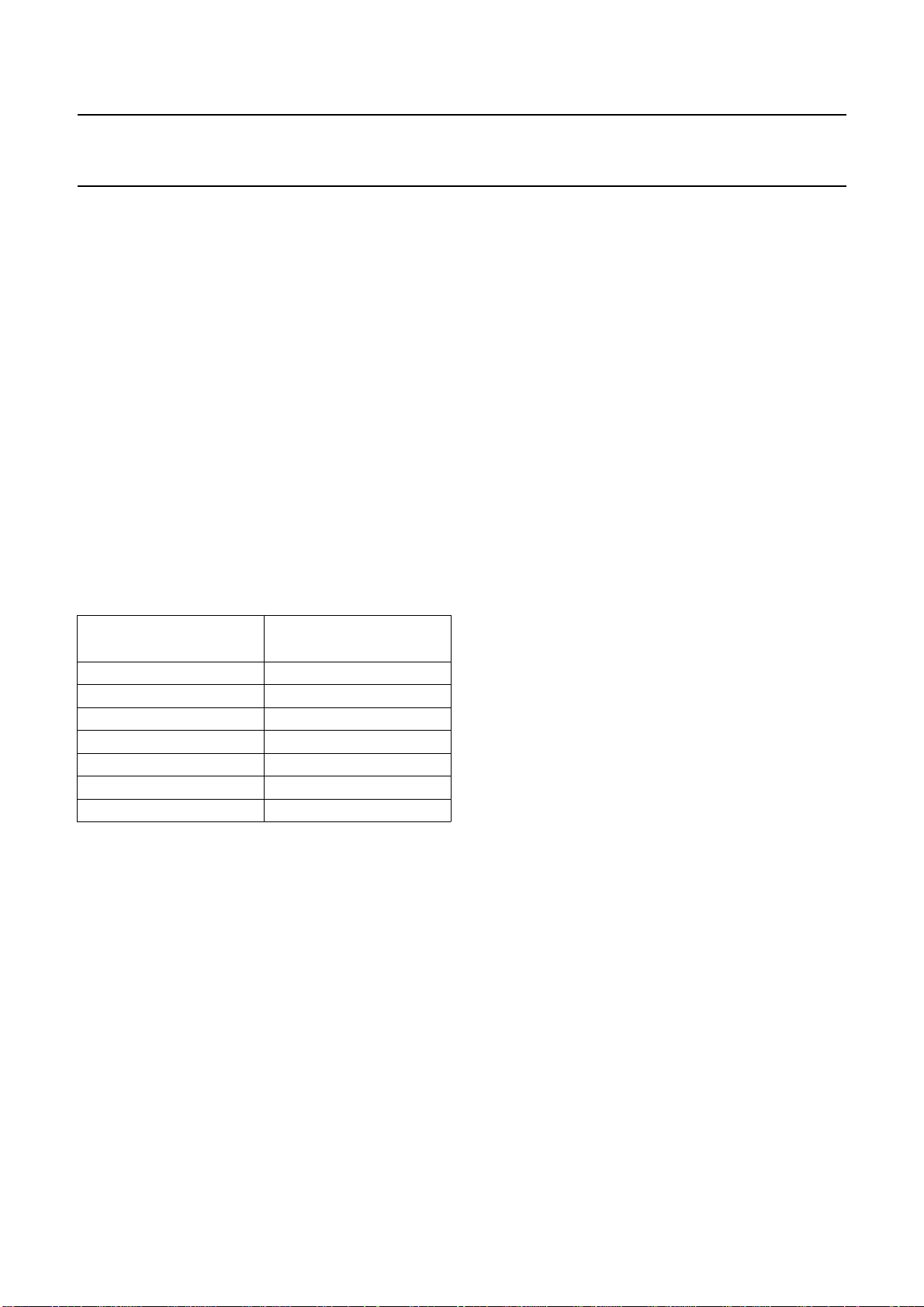
Table 2 Interrupts and vector address
INTERRUPT SOURCE
Reset 000
External INT0 003
Timer 0 00B
External INT1 013
Timer 1 01B
2
Byte I
C-bus 02B
2
Bit I
C-bus 053
7.2.2 O
The SAA5288 does not support the use of off-chip
program memory or off-chip data memory.
“80C51-Based; 8-bit Microcontrollers,
. Using the 80C51 as a reference,
VECTOR ADDRESS
(HEX)
FF-CHIP MEMORY
SAA5288
7.3 Additional features
The following features are provided in addition to the
standard 80C51 features.
7.3.1 I
The external INT1 interrupt is modified to generate an
interrupt on both the rising and falling edges of the INT1
pin, when EX1 bit is set. This facility allows for software
pulse-width measurement for handling of a remote control.
7.3.2 B
For reasons of compatibility with the SAA5290, SAA5291,
SAA5291A and SAA5491 all contain a bit level serial I/O
which supports the I2C-bus. P1.6/SCL and P1.7/SDA are
the serial I/O pins. These two pins meet the I2C-bus
specification concerning the input levels and output drive
capability see
specifications)”
open-drain output configuration. All the four following
modes of the I2C-bus are supported.
• Master transmitter
• Master receiver
• Slave transmitter
• Slave receiver.
Three SFRs support the function of the bit-level I2C-bus
hardware: S1INT, S1BIT and S1SCS and are enabled by
setting register bit TXT8.I2C SELECT to logic 0.
7.3.3 B
The byte level serial I/O supports the I2C-bus protocol.
P1.6/SCL and P1.7/SDA are the serial I/O pins. These two
pins meet the I2C-bus specification concerning the input
levels and output drive capability. Consequently, these two
pins have an open-drain output configuration.
NTERRUPTS
IT LEVEL I
2
C-BUS INTERFACE
“The I2C-bus and how to use it (including
. Consequently, these two pins have an
YTE LEVEL I
2
C-BUS INTERFACE
7.2.3 I
DLE AND POWER-DOWN MODES
Idle and Power-down modes are not supported.
Consequently, the respective bits in PCON are not
available.
7.2.4 UART
FUNCTION
The 80C51 UART is not available. As a consequence the
SCON and SBUF SFRs are removed and the ES bit in the
IE SFR is unavailable.
1997 Jun 24 8
The byte level I2C-bus serial port is identical to the I2C-bus
serial port on the 8xC552. The operation of the subsystem
is described in detail in the 8xC552 data sheet described
in
“80C51-Based; 8-bit Microcontrollers Data Handbook
IC20”
.
Four SFRs support the byte level I2C-bus hardware:
S1CON, S1STA, S1DAT and S1ADR. They are enabled
by setting register bit TXT8. I2C SELECT to logic 1.
7.3.4 LED
SUPPORT
Port pins P0.5 and P0.6 have a 10 mA current sinking
capability to enable LEDs to be driven directly.
Page 9

Philips Semiconductors Preliminary specification
TV microcontroller with full screen
SAA5288
On Screen Display (OSD)
7.3.5 6-BIT PWM DACS
Eight 6-bit DACs are available to allow direct control of analogue sections of the television.
Each low resolution 6-bit DAC is controlled by its associated Special Function Register (PWM0 to PWM7). The PWM
outputs are alternative functions of Port 2 and P3.4. The PWE bit in the SFR for the port corresponding to the PWM
should be set to logic 1 for correct operation of the PWM, e.g. if PWM0 is to be used, P2.1 should be set to logic 1 setting
the port pin to high-impedance.
7.3.5.1 Pulse Width Modulator Registers (PWM0 to PWM7)
Table 3 Pulse Width Modulator Registers (see Table 10 for addresses)
76543210
PWE − PV5 PV4 PV3 PV2 PV1 PV0
Table 4 Description of PWMn bits (n=0to7)
BIT SYMBOL DESCRIPTION
7 PWE If PWE is set to a logic 1, the corresponding PWM is active and controls its assigned
port pin. If PWE is set to la logic 0, the port pin is controlled by the corresponding bit in
the port SFR.
6 − not used
5 PV5 The output of the PWM is a pulse of period 21.33 µs with a pulse HIGH time determined
4 PV4
3 PV3
2 PV2
1 PV1
0 PV0
by the binary value of these 6-bits multiplied by 0.33 µs. PV5 is the most significant bit.
1997 Jun 24 9
Page 10
Philips Semiconductors Preliminary specification
TV microcontroller with full screen
SAA5288
On Screen Display (OSD)
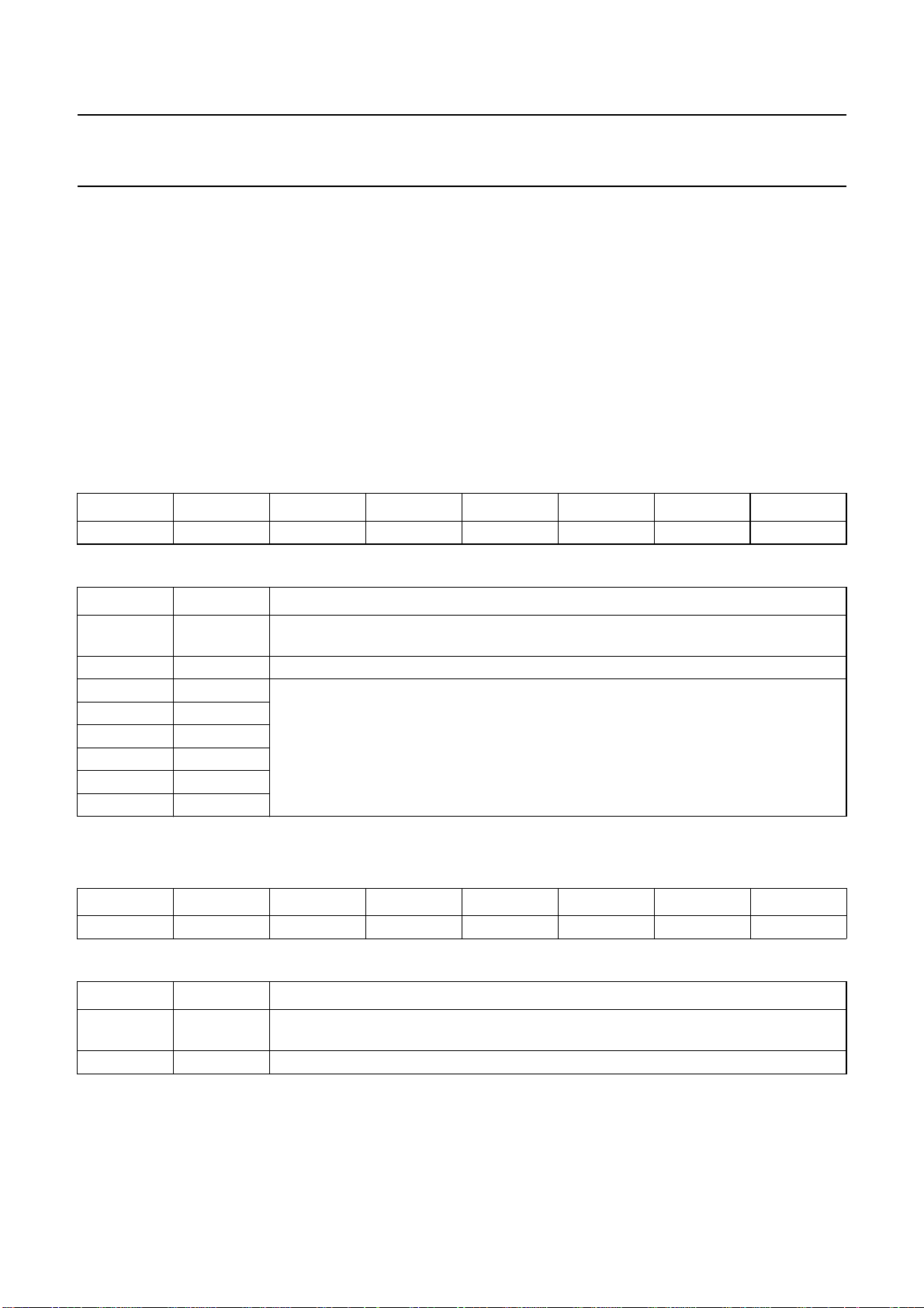
7.3.6 14-BIT PWM DAC
One 14-bit DAC is available to allow direct control of analogue sections of the television. The 14-bit PWM is controlled
using Special Function Registers TDACL and TDACH.
The output of the TPWM is a pulse of period 42.66 µs. The 7 most significant bits, TDACH.TD13 (MSB) to TDACH.TD8
and TDACL.TD7, alter the pulse width between 0 and 42.33 µs, in much the same way as in the 6-bit PWMs. The 7 least
significant bits, TDACL.TD6 to TDACL.TD0 (LSB), extend certain pulses by a further 0.33 µs, e.g. if the 7 least significant
bits are given the value 01H, then 1 in 128 cycles is extended. If the 7 least significant bits are given the value 02H, then
2 in 128 cycles is extended, and so forth.
The TPWM will not start to output a new value until after writing a value to TDACH. Therefore, if the value is to be
changed, TDACL should be written to before TDACH.
7.3.6.1 TPWM High Byte Register (TDACH)
Table 5 TPWM High Byte Register (SFR address D3H)
76543210
PWE − TD13 TD12 TD11 TD10 TD9 TD8
Table 6 Description of TDACH bits
BIT SYMBOL DESCRIPTION
7 PWE If PWE is set to a logic 1, the TPWM is active and controls port line P2.0. If PWE is set
to a logic 0, the port pin is controlled by the corresponding bit in the port SFR.
6 − not used
5 TD13 These 6-bits along with bit TD7 in the TDACL register control the pulse width period.
4 TD12
3 TD11
2 TD10
1 TD9
0 TD8
7.3.6.2 TPWM Low Byte Register (TDACL)
Table 7 TPWM Low Byte Register (SFR address D2H)
76543210
TD7 TD6 TD5 TD4 TD3 TD2 TD1 TD0
Table 8 Description of TDACL bits
BIT SYMBOL DESCRIPTION
7 TD7 This bit is used with bits TD13 to TD8 in the TDACH register to control the pulse width
6 to 0 TD6 to TD0 These 7-bits extend certain pulses by a further 0.33 µs.
TD13 is the most significant bit.
period.
1997 Jun 24 10
Page 11
Philips Semiconductors Preliminary specification
TV microcontroller with full screen
On Screen Display (OSD)
7.3.7 SOFTWARE ADC
Up to 4 successive approximation ADCs can be
implemented in software by making use of the on-chip 8-bit
DAC and multiplexed voltage comparator. The software
ADC uses 4 analog inputs which are multiplexed with P3.0
to P3.3.
Table 9 ADC input channel selection
CH1 CH0 INPUT PIN
0 0 P3.3/ADC3
0 1 P3.0/ADC0
1 0 P3.1/ADC1
1 1 P3.2/ADC2
SAA5288
The control of the ADC is achieved using the Special
Function Registers SAD and SADB.
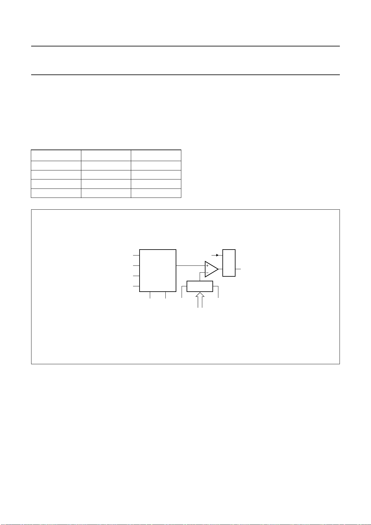
SAD.CH1 and SAD.CH0 select one of the four inputs to
pass to the comparator. The other comparator input
comes from the DAC, whose value is set by SAD.SAD7
(MSB) to SAD.SAD4 and SADB.SAD3 to SADB.SAD0
(LSB). The setting of the value SAD.SAD7 to SAD.SAD4
must be performed at least 1 instruction cycle before the
setting of SAD.ST to ensure comparison is made using the
correct SAD.SAD7 to SAD.SAD4 value.
The output of the comparator is SAD.VHI, and is valid after
1 instruction cycle following the setting of SAD.ST to
logic 1.
handbook, halfpage
P3.0
P3.1
P3.2
P3.3
MULTIPLEXER
8-BIT DAC
CH1, CH0
SAD7 to SAD0
Fig.3 SAD block diagram.
ST C1
1D
REF+REF−
VH1
MGL115
1997 Jun 24 11
Page 12
1997 Jun 24 12
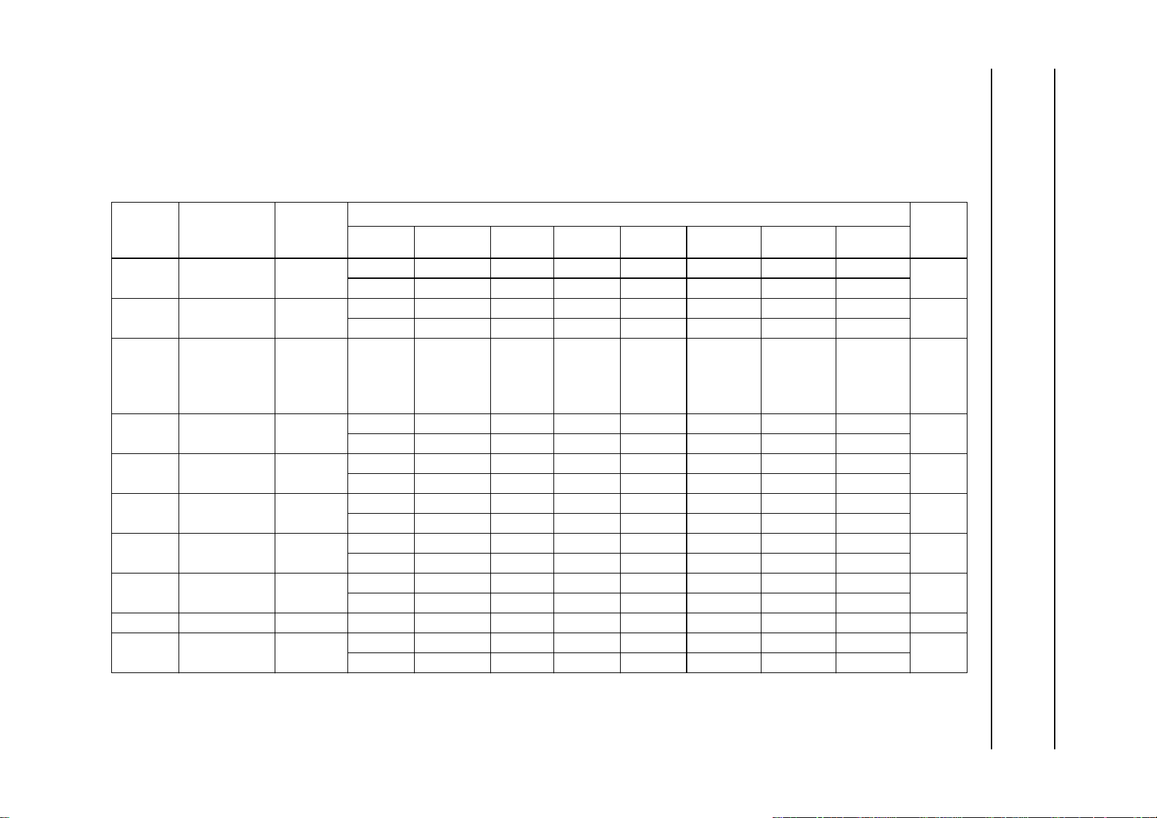
7.4 Microcontroller Interfacing
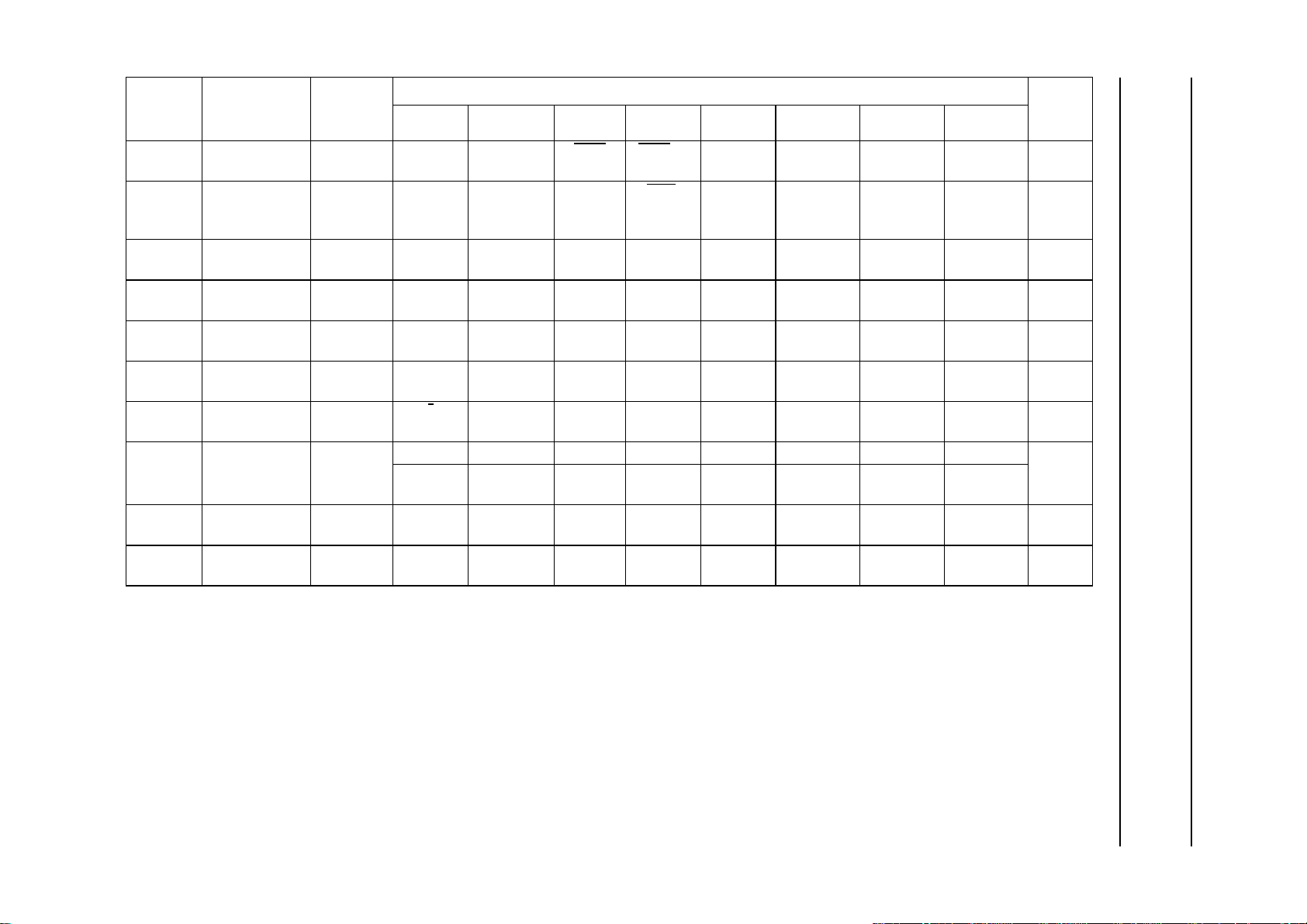
The 80C51 communicates with the peripheral functions using Special Function Registers which are addressed as RAM locations. The registers in the
teletext decoder appear as normal SFRs in the microcontroller memory map, but are written to using an internal serial bus. The SFR map is given in
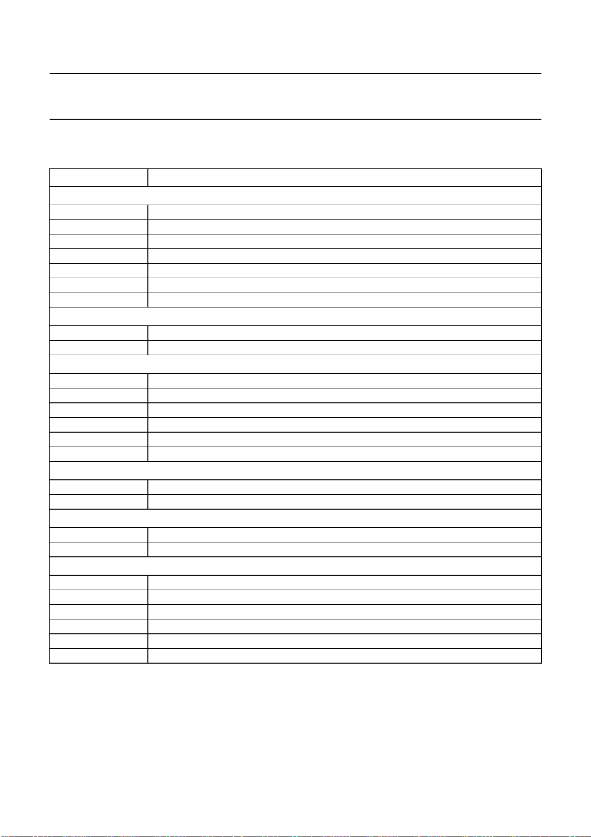
Section 7.4.1 and the SFR bit description is given in Section 7.4.2.
Philips Semiconductors Preliminary specification
TV microcontroller with full screen
On Screen Display (OSD)
7.4.1 S
PECIAL FUNCTION REGISTER MAP
Table 10 Special Function Register map; note 1
BIT ADDRESS, SYMBOL OR ALTERNATIVE PORT FUNCTION RESET
VALUE
(HEX)
SYMBOL NAME
(2)
ACC
Accumulator E0 E7 E6 E5 E4 E3 E2 E1 E0 00
DIRECT
ADDRESS
(HEX)
76543210
−−−−−−−−
(2)
B
B register F0 F7 F6 F5 F4 F3 F2 F1 F0 00
−−−−−−−−
DPTR: Data Pointer
(2 bytes):
DPH High byte 83 −−−−−−−−00
DPL Low byte 82 −−−−−−−−00
(2)(3)
IE
P0
(2)
Interrupt
Enable
A8 AF AE AD AC AB AA A9 A8 00
EA ES1 ES2 * ET1 EX1 ET0 EX0
Port 0 80 87 86 85 84 83 82 81 80 FF
−−−−−−−−
P1
(2)
Port 1 90 97 96 95 94 93 92 91 90 FF
−−−−−−−−
P2
(2)
Port 2 A0 A7 A6 A5 A4 A3 A2 A1 A0 FF
−−−−−−−−
P3
(2)(3)
Port 3 B0 −−−−B3 B2 B1 B0 FF
−−−−−−−−
(3)
PCON
PSW
Power Control 87 − * − * GF1 GF0 −−10
(2)
Program
Status Word
D0 D7 D6 D5 D4 D3 D2 D1 D0 00
CY AC F0 RS1 RS0 OV * P
SAA5288
Page 13

1997 Jun 24 13
SYMBOL NAME
(3)
PWM0
(3)
PWM1
(3)
PWM2
(3)
PWM3
(3)
PWM4
(3)
PWM5
(3)
PWM6
(3)
PWM7
S1ADR
(3)
S1CON
(2)(3)(4)
S1SCS
(2)(3)(5)
S1DAT
(3)(4)
S1INT
(3)(5)
S1STA
(3)(4)
S1BIT
(3)(5)
Pulse Width
Modulator 0
Pulse Width
Modulator 1
Pulse Width
Modulator 2
Pulse Width
Modulator 3
Pulse Width
Modulator 4
Pulse Width
Modulator 5
Pulse Width
Modulator 6
Pulse Width
Modulator 7
Serial I2C-bus
address
Serial I2C-bus
control
Serial I2C-bus
control
Serial I2C-bus
data
Serial I2C-bus
Interrupt
Serial I2C-bus
status
Serial I2C-bus
data
DIRECT
BIT ADDRESS, SYMBOL OR ALTERNATIVE PORT FUNCTION RESET
ADDRESS
(HEX)
76543210
D5 PWE * PV5 PV4 PV3 PV2 PV1 PV0 40
D6 PWE * PV5 PV4 PV3 PV2 PV1 PV0 40
D7 PWE * PV5 PV4 PV3 PV2 PV1 PV0 40
DC PWE * PV5 PV4 PV3 PV2 PV1 PV0 40
DD PWE * PV5 PV4 PV3 PV2 PV1 PV0 40
DE PWE * PV5 PV4 PV3 PV2 PV1 PV0 40
DF PWE * PV5 PV4 PV3 PV2 PV1 PV0 40
D4 PWE * PV5 PV4 PV3 PV2 PV1 PV0 40
DB ADR6 ADR5 ADR4 ADR3 ADR2 ADR1 ADR0 GC 00
D8 DF DE DD DC DB DA D9 D8
CR2 ENSI STA STO SI AA CR1 CR0 00
D8 DF DE DD DC DB DA D9 D8
SDI SCI CLH BB RBF WBF STR ENS E0
DA DAT7 DAT6 DAT5 DAT4 DAT3 DAT2 DAT1 DAT0 00
DA SI −−−−−−−7F
D9 STAT4 STAT3 STAT2 STAT1 STAT0 0 0 0 F8
D9 SDO/SDI −−−−−−−7F
VALUE
(HEX)
Philips Semiconductors Preliminary specification
TV microcontroller with full screen
On Screen Display (OSD)
SAA5288
Page 14

1997 Jun 24 14
BIT ADDRESS, SYMBOL OR ALTERNATIVE PORT FUNCTION RESET
SYMBOL NAME
(2)(3)
SAD
Software ADC
(MSB)
SADB
(2)(3)
Software ADC
(LSB)
DIRECT
ADDRESS
(HEX)
76543210
E8 EF EE ED EC EB EA E9 E8 00
VHI CH1 CH0 ST SAD7 SAD6 SAD5 SAD4
98 9F 9E 9D 9C 9B 9A 99 98 00
−−−−SAD3 SAD2 SAD1 SAD0
SP Stack Pointer 81 8F 8E 8D 8C 8B 8A 89 88 07
(2)
TCON
Timer/counter
88 TF1 TR1 TF0 TR0 IE1 IT1 IE0 IT0 00
control
TDACH TPWM High
D3 PWE * TD13 TD12 TD11 TD10 TD9 TD8 40
byte
TDACL TPWM Low
D2 TD7 TD6 TD5 TD4 TD3 TD2 TD1 TD0 00
byte
TH0 Timer 0 High
8C TH07 TH06 TH05 TH04 TH03 TH02 TH01 TH00 00
byte
TH1 Timer 1 High
8D TH17 TH16 TH15 TH14 TH13 TH12 TH11 TH10 00
byte
TL0 Timer 0 Low
8A TL07 TL06 TL05 TL04 TL03 TL02 TL01 TL00 00
byte
TL1 Timer 1 Low
8B TL17 TL16 TL15 TL14 TL13 TL12 TL11 TL10 00
byte
TMOD Timer/counter
mode
(3)
TXT0
Teletext
Register 0
89 GATE C/
TM1M0GATEC/TM1M000
Timer 1 Timer 0
C0 * * AUTO
FRAME
* DISPLAY
STATUS
DISABLE
FRAME
**00
ROW
ONLY
(3)
TXT1
TXT4
TXT5
(3)
(3)
Teletext
Register 1
Teletext
Register 4
Teletext
Register 5
C1 * * * * * FIELD
POLARITYHPOLARITYVPOLARITY
C4 * * EAST/
WEST
C5 BKGND
OUT
BKGND IN COR
OUT
DISABLE
DBL HT
B MESH
ENABLE
COR IN TEXT
OUT
C MESH
ENABLE
TEXT IN PICTURE
TRANS
ENABLE
ON OUT
SHADOW
ENABLE
PICTURE
ON IN
VALUE
(HEX)
00
00
03
Philips Semiconductors Preliminary specification
TV microcontroller with full screen
On Screen Display (OSD)
SAA5288
Page 15
1997 Jun 24 15
SYMBOL NAME
(3)
TXT6
(3)
TXT7
(3)
TXT8
(3)
TXT9
(3)
TXT10
(3)
TXT11
(3)
TXT12
TXT13
(2)(3)
(3)
TXT16
(3)
TXT17
Teletext
Register 6
Teletext
Register 7
T eletext
Register 8
Teletext
Register 9
Teletext
Register 10
Teletext
Register 11
Teletext
Register 12
Teletext
Register 13
Teletext
Register 16
Teletext
Register 17
DIRECT
BIT ADDRESS, SYMBOL OR ALTERNATIVE PORT FUNCTION RESET
ADDRESS
(HEX)
C6 BKGND
C7 STATUS
76543210
OUT
ROW
BKGND IN COR
OUT
CURSORONREVEAL
COR IN TEXT
OUT
TOP/
BOTTOM
DOUBLE
HEIGHT
TEXT IN PICTURE
ON OUT
BOX ON24BOX ON
1−23
PICTURE
ON IN
BOX ON
0
TOP
C8 I2C
** *****00
SELECT
C9 CURSOR
FREEZE
CLEAR
MEMORY
*R4R3R2R1R000
CA * * C5 C4 C3 C2 C1 C0 00
CB D7 D6 D5 D4 D3 D2 D1 D0 00
CC * ROM VERR4ROM
VER R3
ROM
VER R2
ROM
VER R1
ROM VERR0TXT ON * 0XXXX
B8 BF BE BD BC BB BA B9 B8 00
* PAGE
CLEARING
525
DISPLAY
* * * * OSD I/F
busy
CF * Y2 Y1 Y0 * * X1 X0 00
B9 * * * FORCE
625
FORCE
525
SCREEN
COL2
SCREEN
COL1
SCREEN
COL0
VALUE
(HEX)
03
00
X00B
00
Philips Semiconductors Preliminary specification
TV microcontroller with full screen
On Screen Display (OSD)
Notes
1. The asterisk (*) indicates these bits are inactive and must be written to logic 0 for future compatibility.
2. SFRs are bit addressable.
3. SFRs are modified or added to the 80C51 SFRs.
4. This register is used for Byte Orientated I2C-bus, TXT8. I2C SELECT = 1.
5. This register is used for Bit Orientated I2C-bus, TXT8. I2C SELECT = 0.
SAA5288
Page 16
Philips Semiconductors Preliminary specification
TV microcontroller with full screen
On Screen Display (OSD)
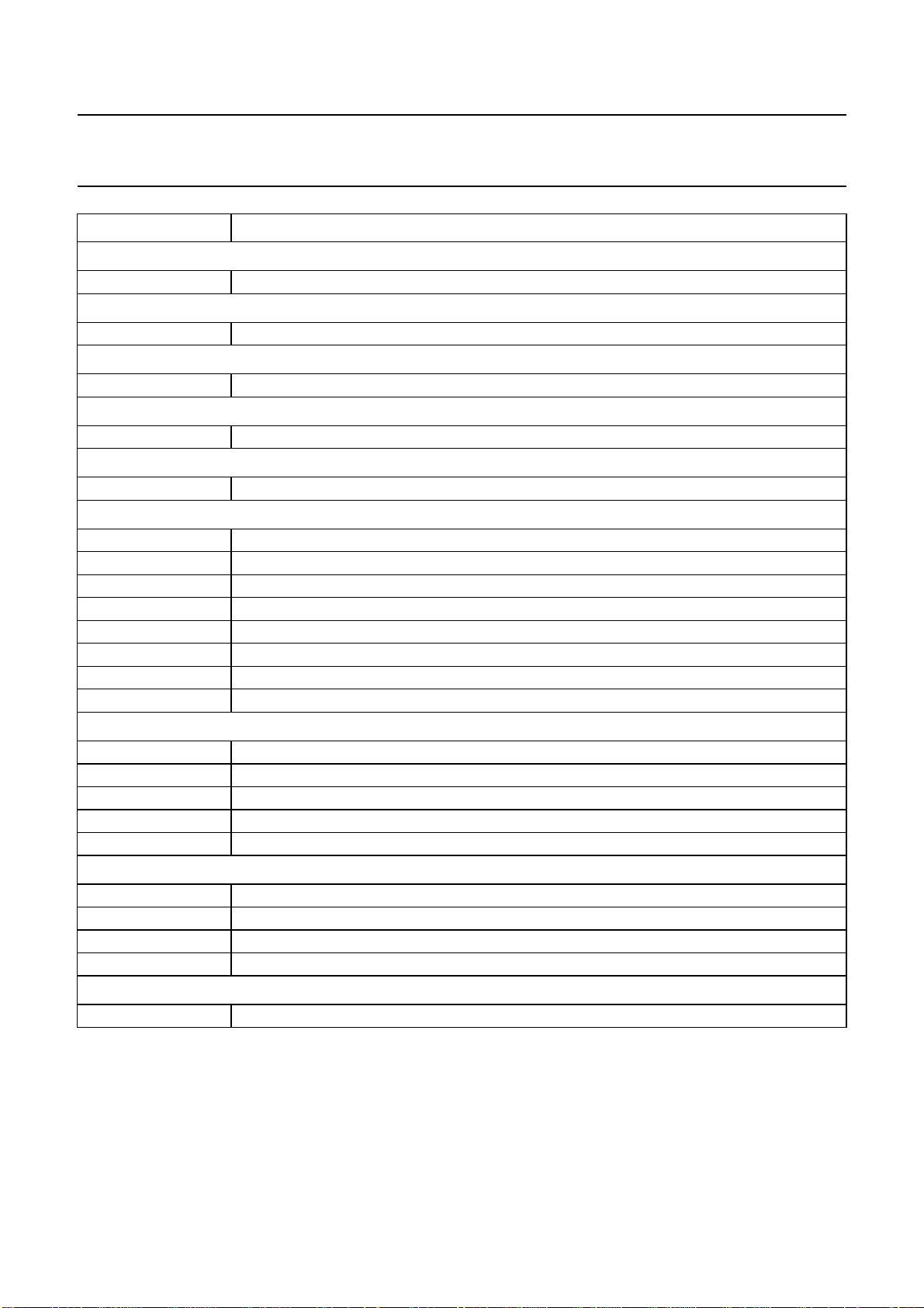
7.4.2 SPECIAL FUNCTION REGISTERS BIT DESCRIPTION
Table 11 SFR bit descriptions
REGISTER FUNCTION
Interrupt Enable Register (IE)
EA disable all interrupts (logic 0) or use individual interrupt enable bits (logic 1)
2
ES1 bit I
ES2 byte I
ET1 enable Timer 1 overflow interrupt (logic 1)
EX1 enable external interrupt 1 (logic 1)
ET0 enable Timer 0 overflow interrupt (logic 1)
EX0 enable external interrupt 0 (logic 1)
Power Control Register (PCON)
GF1 general purpose flag 1
GF0 general purpose flag 0
Program Status Word (PSW)
CY carry flag
AC auxiliary carry flag
F0 flag 0
RS1, RS0 register bank select control bits
OV overflow flag
P parity flag
C-bus interrupt enable (logic 1)
2
C-bus interrupt enable (logic 1)
SAA5288
6-bit Pulse Width Modulator Control Registers (PWM0 to PWM7)
PWE activate this PWM and take control of respective port pin (logic 1)
PV5 to PV0 binary value sets high time of PWM output
Serial Interface Slave Address Register (S1ADR)
ADR6 to ADR0 I
GC enables response to the I
Serial Interface Control Register (S1CON)
CR2 to CR0 clock rate bits
ENSI I
STA start condition flag
STO stop condition flag
SI interrupt flag
AA assert acknowledge flag
2
C-bus slave address to which the device will respond
2
C-bus general call address
2
C-bus interface enable
1997 Jun 24 16
Page 17
Philips Semiconductors Preliminary specification
TV microcontroller with full screen
On Screen Display (OSD)
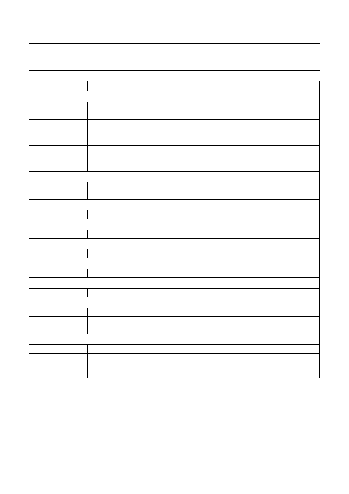
REGISTER FUNCTION
Serial Interface Data Register (S1DAT)
2
DAT7 to DAT0 I
Serial Interface Status Register (S1STA) - READ only
STAT4 to STAT0 I
Serial Interface Data Register (S1BIT) - READ
SDI I2C-bus data bit input
Serial Interface Data Register (S1BIT) - WRITE
SDO I2C-bus data bit output
Serial Interface Interrupt Register (S1INT)
SI I2C-bus interrupt flag
Serial Interface Control Register (S1SCS) - READ
SDI serial data input at SDA
SCI serial clock input at SCL
CLH clock LOW-to-HIGH transition flag
BB bus busy flag
RBF read bit finished flag
WBF write bit finished flag
STR clock stretching enable (logic 1)
ENS enable serial I/O (logic 1)
C-bus data
2
C-bus interface status
SAA5288
Serial Interface Control Register (S1SCS) - WRITE
SDO serial data output at SDA
SCO serial clock output at SCL
CLH clock LOW-to-HIGH transition flag
STR clock stretching enable (logic 1)
ENS enable serial I/O (logic 1)
Software ADC Control Register (SAD)
VHI comparator output indicating that analogue input voltage greater than DAC voltage (logic 1)
CH1 and CH0 ADC input channel selection bits, see Table 11
ST initiate voltage comparison (logic 1); this bit is automatically reset to logic 0
SAD7 to SAD4 4 MSB’s of DAC input value
Software ADC Control Register (SADB)
SAD3 to SAD0 4 LSB’s of DAC input value
1997 Jun 24 17
Page 18
Philips Semiconductors Preliminary specification
TV microcontroller with full screen
On Screen Display (OSD)
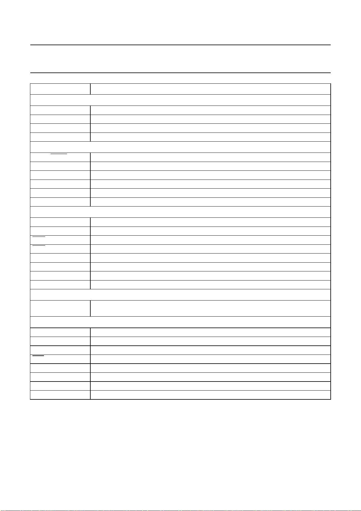
REGISTER FUNCTION
Timer/Counter Control Register (TCON)
TF1 Timer 1 overflow flag
TR1 Timer 1 run control bit
TF0 Timer 0 overflow flag
TR0 Timer 0 run control bit
IE1 Interrupt 1 edge flag
IT1 Interrupt 1 type control bit
IE0 Interrupt 0 edge flag
IT0 Interrupt 0 type control bit
14-bit PWM MSB Register (TDACH)
PWE activate this 14-bit PWM and take over port pin (logic 1)
TD13 to TD8 6 MSBs of 14-bit number to be output by the 14-bit PWM
14-bit PWM LSB Register (TDACL)
TD7 to TD0 8 LSBs of 14-bit number to be output by the 14-bit PWM
SAA5288
Timer 0 High byte (TH0)
TH07 to TH00 8 MSBs of Timer 0 16-bit counter
Timer 1 High byte (TH1)
TH17 to TH10 8 MSBs of Timer 1 16-bit counter
Timer 0 Low byte (TL0)
TL07 to TL00 8 LSBs of Timer 0 16-bit counter
Timer 1 Low byte (TL1)
TL17 to TL10 8 LSBs of Timer 1 16-bit counter
Timer/Counter Mode Control Register (TMOD)
GATE gating control
C/
T counter or timer selector
M1, M0 mode control bits
Teletext Register 0 (TXT0) - WRITE only
AUTO FRAME FRAME output switched off automatically if any video displayed (logic 1)
DISPLAY STATUS
ROW ONLY
DISABLE FRAME FRAME output always low (logic 1)
display row 24 only (logic 1)
1997 Jun 24 18
Page 19
Philips Semiconductors Preliminary specification
TV microcontroller with full screen
SAA5288
On Screen Display (OSD)
REGISTER FUNCTION
Teletext Register 1 (TXT1) - WRITE only
FIELD POLARITY VSYNC in first half of the line (logic 0) or second half of the line (logic 1) at start of even field
H POLARITY HSYNC input positive-going (logic 0) or negative-going (logic 1)
V POLARITY VSYNC input positive-going (logic 0) or negative-going (logic 1)
PRD4 to PRD0 page request data
Teletext Register 4 (TXT4) - WRITE only
EAST/
WEST western languages selected (logic 0) or Eastern languages selected (logic 1)
DISABLE DBL HGHT disable display of double height teletext control codes (logic 1) in OSD boxes
B MESH ENABLE enable meshing of area with black background (logic 1)
C MESH ENABLE enable meshing of area with other background colours (logic 1)
TRANS ENABLE set black background to transparent i.e. video is displayed (logic 1)
SHADOW ENABLE enable south-east shadowing (logic 1)
Teletext Register 5 (TXT5) - WRITE only
BKGND OUT background colour displayed outside teletext boxes (logic 1)
BKGND IN background colour displayed inside teletext boxes (logic 1)
COR OUT COR output active outside teletext boxes (logic 1)
COR IN COR output active inside teletext boxes (logic 1)
TEXT OUT text displayed outside teletext boxes (logic 1)
TEXT IN text displayed inside teletext boxes (logic 1)
PICTURE ON OUT video picture displayed outside teletext boxes (logic 1)
PICTURE ON IN video picture displayed inside teletext boxes (logic 1)
Teletext Register 6 (TXT6) - WRITE only
See TXT5 this register has the same meaning as TXT5 but is only invoked if either newsflash (C5) or
subtitle (C6) bit in row 25 of the basic page memory is set
Teletext Register 7 (TXT7) - WRITE only
STATUS ROW TOP display row 24 below (logic 0) or above (logic 1) teletext page
CURSOR ON display cursor at location pointed to by TXT9 and TXT10 (logic 1)
REVEAL display characters in areas with the conceal attribute set (logic 1)
TOP/BOTTOM display rows 0 to 11 (logic 0) or 12 to 23 (logic 1) when the double height bit is set
DOUBLE HEIGHT display each character as twice normal height (logic 1)
BOX ON 24 enable teletext boxes in memory row 24 (logic 1)
BOX ON 1-23 enable teletext boxes in memory rows 1 to 23 (logic 1)
BOX ON 0 enable teletext boxes in memory row 0 (logic 1)
1997 Jun 24 19
Page 20
Philips Semiconductors Preliminary specification
TV microcontroller with full screen
SAA5288
On Screen Display (OSD)
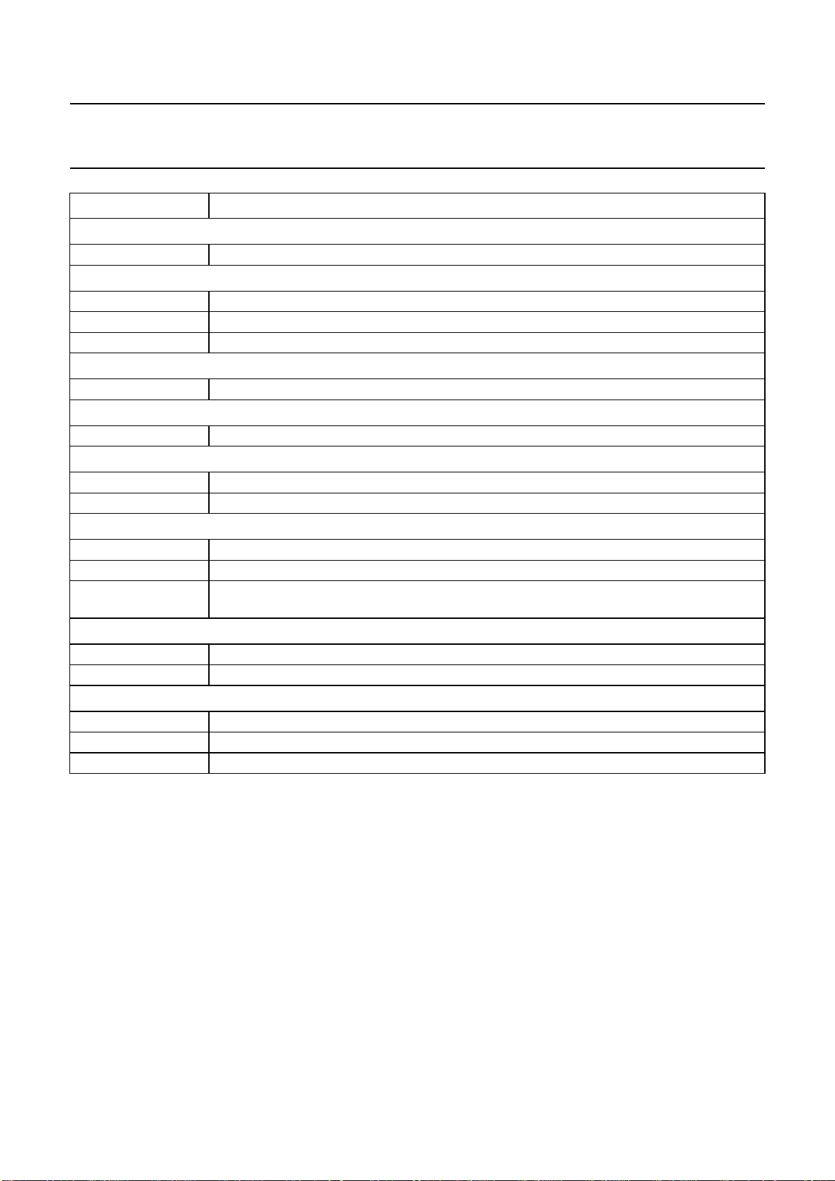
REGISTER FUNCTION
Teletext Register 8 (TXT8)
2
C SELECT select bit I2C-bus (logic 0) or byte I2C-bus (logic 1)
I
Teletext Register 9 (TXT9) - WRITE only
CURSOR FREEZE locks current cursor position (logic 1)
CLEAR MEMORY write 20H into every location in display memory (logic 1)
R4 to R0 memory row to be accessed by TXT11
Teletext Register 10 (TXT10) - WRITE only
C5 to C0 memory column to be accessed by TXT11
Teletext Register 11 (TXT11)
D7 to D0 data byte written to, or read from display memory
Teletext Register 12 (TXT12) - READ only
ROM VER R4 to R0 mask programmable identification for character set
DISPLAY ON power has been applied to the display hardware (logic 1)
Teletext Register 13 (TXT13)
PAGE CLEARING set when software requested page clear in progress
525 DISPLAY set to logic 1 when 525-line syncs are driving the display
OSD I/F Busy OSD interface busy; logic 1 indicates that TXT Registers 0 to 16 can not currently be
accessed
Teletext Register 16 (TXT16) - WRITE only
Y2 to Y0 sets vertical position of display area
X1 to X0 sets horizontal position of display area
Teletext Register 17 (TXT17) - Write only
FORCE 625 force display to 625-line mode
FORCE 525 force display to 525-line mode
SCREEN COL 2 to 0 defines colour displayed instead of TV picture and black background
1997 Jun 24 20
Page 21
Philips Semiconductors Preliminary specification
TV microcontroller with full screen
On Screen Display (OSD)
7.5 The display
7.5.1 I
The capabilities of the display are based on the
requirements of level 1 teletext, with some enhancements
for use with locally generated on screen displays.
The display consists of 25 rows each of 40 characters,
with the characters displayed being those from rows
0 to 24 of the basic page memory. If the TXT.7 STATUS
ROW TOP bit is set row 24 is displayed at the top of the
screen, followed by row 0, but normally memory rows are
displayed in numerical order.
The display memory stores 8-bit character codes which
correspond to a number of displayable characters and
control characters, which are normally displayed as
spaces. The character set of the device is described in
more detail in Section 8.
7.5.2 C
Each character is defined by a matrix 12 pixels wide and
10 pixels high. When displayed, each pixel is1⁄12ms wide
and 1 TV line, in each field, high.
NTRODUCTION
HARACTER MATRIX
SAA5288
7.5.3 P
Columns 0 to 9 of row 25 of the memory are treated by the
display as if they contain display control information from
teletext page headers. The bits which affect the display are
shown in Table 12. Columns 0 to 4 are not used.
If C5 (newsflash) or C6 (subtitle) is set the display uses the
display mode defined in register TXT6. C7 (suppress
header) causes the header row (row 0) to be displayed as
if every character was a space. C10 (inhibit display)
displays every character on all rows as if it was a space.
C12 to C14 (language control bits) cause certain character
codes to be interpreted differently (see Section 7.5.5).
Table 12 Page attributes
COLUMN
AGE ATTRIBUTES
PAGE ATTRIBUTE FIELD
76543210
50000C6C500
6 0 0 0 0 C10 0 0 C7
7 0 0 0 0 C14 C13 C12 0
8 00000000
9 00000000
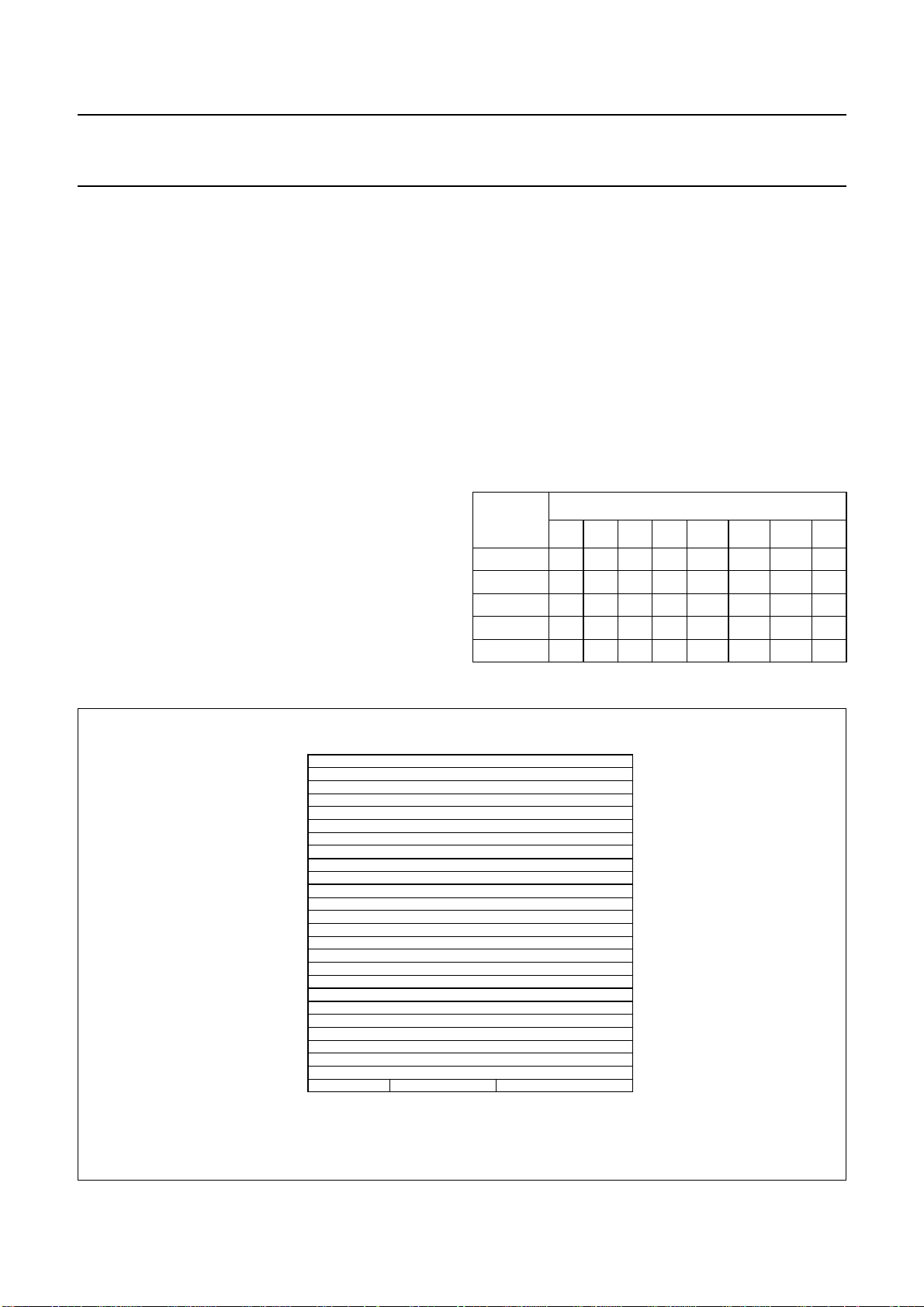
handbook, full pagewidth
ROW 0
1
2
3
4
5
6
7
8
9
10
11
12
13
14
15
16
17
18
19
20
21
22
23
24
page attributes
25
09 23
Fig.4 Display page organisation.
390 DISPLAY PAGE MEMORY
MGL116
1997 Jun 24 21
Page 22

Philips Semiconductors Preliminary specification
TV microcontroller with full screen
On Screen Display (OSD)
7.5.4 EAST/WEST SELECTION
In common with their predecessors, these devices store
teletext pages as a series of 8-bit character codes which
are interpreted as either control codes (to change colour,
invoke flashing etc.) or displayable characters. When the
control characters are excluded, this gives an addressable
set of 212 characters at any given time.
More characters than this were required to give the
language coverage required from the first version of the
device. The TXT4. East/West bit was introduced to allow
the meanings of character codes D0H to FFH to be
changed, depending on where in Europe the device was to
be used. This bit is still used with the other language
variants, although the name East/
much sense.
7.5.5 N
The interpretation of some character codes between 20H
and 7FH depends on the C12 to C14 language control bits
stored in row 25 of the display page.
The interpretation of the C12 to C14 language control bits
is dependant on the East/West bit.
7.6 The twist attribute
In many of the character sets, the ‘twist’ serial attribute
(code 1BH) can be used to switch to an alternative basic
character code table, e.g. to change from the Hebrew
alphabet to the Arabic alphabet on an Arabic/Hebrew
device. For some national option languages the alternative
code table is the default, and a twist control character will
switch to the first code table.
The display hardware on the devices allows one language
to invoke the alternative code table by default when the
East/
is a logic 1. In all of the character sets defined so far, the
language which invokes the alternative code table is the
same for either setting of the East/West bit.
7.6.1 O
In the character sets, character codes 80H to 9FH are
OSD symbols. An editor is available to allow these
characters to be redefined by the customer.
ATIONAL OPTION CHARACTERS
West register bit is a logic 0 and another when the bit
N SCREEN DISPLAY SYMBOLS
West may not make
SAA5288
7.6.2 L
The devices have a readable register TXT12 which
contains a 5-bit identification code TXT12.ROM VER R4 to
TXT12.ROM VER R0 which is intended for use in
identifying which character set the device is using.
7.6.3 525When used with 525-line display syncs, the devices modify
their displays such that the bottom line is omitted from
each character cell. The character sets have been
designed to be readable under these circumstances and
anyone designing OSD symbols is advised to consider this
mode of operation.
7.6.4 C
Character codes 00H to 1FH, B0H to B7H and
BCH to BFH are interpreted as control characters which
can be used to change the colour of the characters, the
background colour, the size of characters, and various
other features. All control characters are normally
displayed as spaces.
The alphanumerics colour control characters (00H to 07H)
are used to change colour of the characters displayed.
The graphics control characters (10H to 17H) change the
colour of the characters and switch the display into a mode
where the codes in columns 2, 3, 6 and 7 of the character
table (see the character table above) are displayed as the
block mosaic characters in columns 2a, 3a, 6a and 7a.
The display of mosaics is switched off using one of the
alphanumerics colour control characters.
The ‘new background’ character (1DH) the background
colour of the display sets the background colour equal to
the current foreground colour. The ‘black background’
character (1CH) changes the background colour to black
independently of the current foreground colour.
The background colour control characters in the upper half
of the code table (B0H to B7H) are additions to the normal
display control characters which allow the background
colour to be changed to any colour with a single control
character and independently of the foreground colour.
The background colour is changed from the position of the
background colour control character.
ANGUAGE GROUP IDENTIFICATION
LINE OPERATION
ONTROL CHARACTERS
1997 Jun 24 22
Page 23
Philips Semiconductors Preliminary specification
TV microcontroller with full screen
On Screen Display (OSD)
Displayable characters between a ‘flash’ (08H) and a
‘steady’ (09H) control character will flash on and off.
Displayable characters between a ‘conceal display’ (18H)
character and an alphanumerics or graphics control
character are displayed as spaces, unless the
TXT7.REVEAL bit is set.
The ‘contiguous graphics’ (19H) and ‘separated graphics’
(1AH) characters control the way in which mosaic shapes
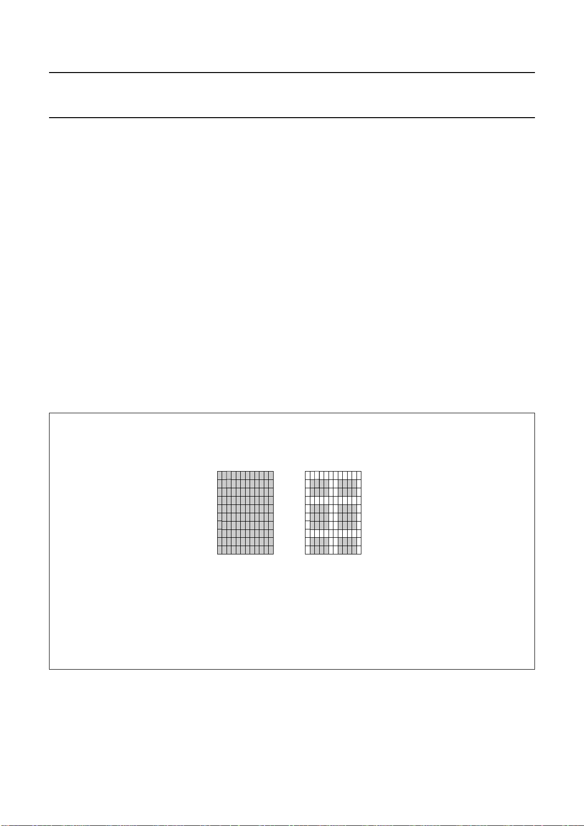
are displayed. The difference between the two is shown in
Fig.5.
Control characters encountered between a ‘hold graphics’
(1EH) control character and a ‘release graphics’ (1FH)
control character are displayed as the last character
displayed in graphics mode, rather than as spaces.
From the hold graphics character until the first character
displayed in graphics mode the held character is a space.
The ‘start box’ (0BH) and ‘end box’ (0AH) characters are
used to define teletext boxes. Two start box characters are
required to begin a teletext box, with the box starting
between the 2 characters. The box ends after an end box
character has been encountered.
SAA5288
The display can be set up so that different display modes
are invoked inside and outside teletext boxes e.g. text
inside boxes but TV outside. This is described in
Section 7.6.5.
The ‘normal size’ (0CH), ‘double height’ (0DH), ‘double
width’ (0EH) and ‘double size’ (0FH) control characters are
used to change the size of the characters displayed. If any
double height (or double size) characters are displayed on
a row the whole of the next row is displayed as spaces.
Double height display is not possible on either row 23 or
row 24.
The character in the position occupied by the right hand
half of a double width (or double size) character is ignored,
unless it is a control character in which case it takes effect
on the next character displayed. This allows double width
to be used to produce a display in which blank spaces do
not appear when character attributes are changed.
The size implying OSD (BCH to BFH) control characters
have been included in this device to allow OSD messages
to be generated easily. These characters are described in
full later in this document.
handbook, halfpage
mosaics character 7FH
contiguous
mosaics character 7FH
Fig.5 Contiguous and separated mosaics.
separated
MGL117
1997 Jun 24 23
Page 24
Philips Semiconductors Preliminary specification
TV microcontroller with full screen
On Screen Display (OSD)
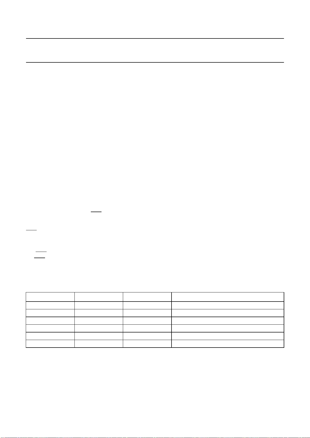
7.6.5 DISPLAY MODES
The device signals the TV’s display circuits to display the
R, G and B outputs of the device, rather than the video
picture, by outputting a logic 1 on the VDS output. The way
in which this signal is switched is controlled by the bits in
the TXT5 and TXT6 SFRs. There are 3 control functions:
text on, background on and picture on. Separate sets of
bits are used inside and outside teletext boxes so that
different display modes can be invoked. Also, different
SFRs are used depending on whether the newsflash (C5)
or subtitle (C6) bits in row 25 of the basic page memory are
set (SFR TXT6) or not (SFR TXT5). This allows the
software to set up the type of display required on
newsflash and subtitle pages (e.g. text inside boxes, TV
picture outside) this will be invoked without any further
software intervention when such a page is acquired.
When teletext box control characters are present in the
page memory, whichever is relevant of the ‘Boxes On Row
0’, ‘Boxes On Row 1 - 23’ and ‘Boxes On Row 24’ SFR bits
in TXT17 must be set if the display mode is to change in
the box. These bits are present to allow boxes in certain
areas of the screen to be disabled so that teletext boxes
can be used for the display of
danger of subtitles in boxes, which may also be in the page
memory, being displayed. The use of teletext boxes for
OSD messages has been superseded in this device by the
OSD box concept, described later, but these bits remain to
allow teletext boxes to be used, if required.
The COR bits in the TXT5 and TXT6 SFRs control when
the COR output of the device is activated (pulled-down).
This output is intended to act on the TV’s display circuits to
reduce the contrast of the video display when it is active.
OSD messages without the
SAA5288
The result of contrast reduction is to improve the
readability of the text in a mixed text and video display.
The bits in the TXT5 and TXT6 SFRs allow the display to
be set up so that, for example, the areas inside teletext
boxes will be contrast reduced when a subtitle is being
displayed but that the rest of the screen will be displayed
as normal video.
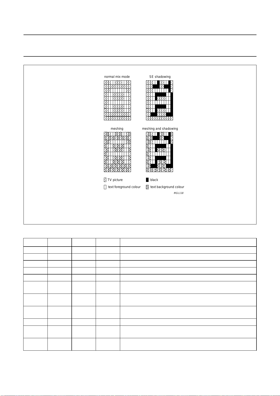
Setting the shadow TXT4.SHADOW ENABLE bit will add
a ‘south east’ shadow to the text, significantly enhancing
its readability in mix mode. Shadowing is shown in Fig.6.
The readability of text can also be enhanced using
‘meshing’. Meshing causes the VDS signal to switch so
that when the text background colour should be displayed
every other pixel is displayed from the video picture. Text
foreground pixels are always displayed.
The TXT4.BMESH bit enables meshing on areas of the
screen within the text display area with black as the
background colour.
The TXT4.CMESH bit has the same effect on areas with
other background colours. Meshing can only be invoked in
areas displayed in text mode i.e. where the TXT5.TEXT IN
and TXT5.BKGND IN bits are both set to logic 1, and in
OSD boxes. Meshed text can also be shadowed. Meshing
is illustrated in Fig.6.
The TXT4.TRANS bit causes areas of black background
colour to become transparent i.e. video is displayed
instead of black background. Black background
transparency can also only be invoked in areas displayed
in text mode i.e. where the TXT5.TEXT IN and
TXT5.BKGND IN bits are both set to logic 1, and in OSD
boxes.
Table 13 Display control bits
PICTURE ON TEXT ON BACKGROUND ON EFFECT
0 0 X text mode, black screen
0 1 0 text mode, background always black
0 1 1 text mode
1 0 X TV mode
1 1 0 mixed text and TV mode
1 1 1 text mode, TV picture outside text area
1997 Jun 24 24
Page 25
Philips Semiconductors Preliminary specification
,
,
,
,
,
,
,
TV microcontroller with full screen
On Screen Display (OSD)
handbook, halfpage
normal mix mode SE shadowing
meshing
SAA5288
meshing and shadowing
TV picture
text foreground colour
black
text background colour
MGL118
Fig.6 Meshing and shadowing.
Table 14 Enhanced display mode selection
SHADOW TRANS BMESH CMESH DISPLAY
0 0 0 0 normal, unshadowed, unmeshed text
0 0 0 1 text with coloured backgrounds meshed, black background solid
0 0 1 0 text with coloured backgrounds solid, black background meshed
0 0 1 1 text with all backgrounds meshed
0 1 X 0 text with coloured backgrounds solid, black background transparent
0 1 X 1 text with coloured backgrounds meshed, black background
transparent
1 0 0 1 shadowed text with coloured backgrounds meshed, black
background solid
1 0 1 0 shadowed text with coloured backgrounds solid, black background
meshed
1 0 1 1 shadowed text with all backgrounds meshed
1 1 X 0 shadowed text with coloured backgrounds solid, black background
transparent
1 1 X 1 shadowed text with coloured backgrounds meshed, black
background transparent
1997 Jun 24 25
Page 26
Philips Semiconductors Preliminary specification
TV microcontroller with full screen
On Screen Display (OSD)
7.7 On Screen Display boxes
The size implying OSD control characters (BCH to BFH)
are intended to allow OSD messages to be displayed.
OSD boxes are not the same as teletext boxes created
using the teletext boxing control characters
(0AH and 0BH).
When one of these characters occurs the display size
changes appropriately (to normal size for BCH, double
height for BDH, double width for BEH and double size for
BFH) and an OSD box starts from the next character
position (‘set after’). The OSD box ends either at the end
of the row of text or at the next size implying OSD
character. When an OSD box is ended using another size
implying OSD character the box ends at the position of the
control character (‘set at’). This arrangement allows
displays to be created without blank spaces at the ends of
the OSD boxes.
To prevent teletext control characters from affecting the
display of the OSD message the flash, teletext box,
conceal, separated graphics, twist and hold graphics
functions are all reset at the start of an OSD box, as they
are at the start of the row. In order to allow the most
commonly used display attributes to be set-up before the
box starts the foreground colour, background colour and
mosaics on/off attributes are not reset.
The text within an OSD box is always displayed in text
mode i.e. as if the Text On and Bkgnd On bits are both set
to a logic 1. The type of display produced inside an OSD
box is, therefore, dependant on the states of the
TXT4.SHADOW ENABLE, TXT4.TRANS ENABLE,
TXT4.BMESH ENABLE and TXT4.CMESH ENABLE
register bits, as described previously. OSD boxes can only
be displayed in TV mode i.e. when the Picture On SFR bit
is a logic 1 and the Text On SFR bit is a logic 0, both inside
and outside text boxes and for both normal and
newsflash/subtitle pages. The display of OSD boxes is not
affected by the C7, suppress header, and C10, inhibit
display, control bits stored in row 25 of the page memory.
SAA5288
7.8 Screen colour
The register bits TXT17.SCREEN COL2-0 can be used to
define a colour to be displayed in place of the TV picture
and the black background colour. If the bits are all set to 0,
the screen colour is defined as ‘transparent’ and the TV
picture and background colour are displayed as normal.
Screen colour is displayed from 10.5 to 62.5 µs after the
active edge of the HSync input and on TV lines 23 to 310
inclusive, for a 625-line display, and lines 17 to 260
inclusive for a 525-line display.
When the screen colour has been redefined, no TV picture
is displayed so the Frame de-interlace output can be
activated, if the SFR bits controlling FRAME are set up to
allow this.
Table 15 Screen colours
SCREEN
COL 2
0 0 0 transparent
001red
0 1 0 green
0 1 1 yellow
1 0 0 blue
1 0 1 magenta
1 1 0 cyan
1 1 1 white
7.9 Cursor
If the TXT7.CURSOR ON bit is set, a cursor is displayed.
The cursor operates by reversing the background and
foreground colours in the character position pointed to by
the active row and column bits in the TXT9 and TXT10
SFRs.
Setting the TXT9.CURSOR FREEZE bit, causes the
cursor to stay in its current position, no matter what
happens to the active row and column positions. This
means that the software can read data from the memory
(e.g. TOP table information) without affecting the position
of the cursor.
SCREEN
COL 1
SCREEN
COL 0
SCREEN
COLOUR
1997 Jun 24 26
Page 27
Philips Semiconductors Preliminary specification
TV microcontroller with full screen
On Screen Display (OSD)
7.10 Other display features
Setting the TXT7.DOUBLE HEIGHT bit causes the normal
height of all display characters to be doubled and the
whole of the display area to be occupied by half of the
display rows. Characters normally displayed double height
will be displayed quadruple height when this bit is set.
Rows 12 to 24 can be enlarged, rather than rows 0 to 11,
by setting the TXT7.TOP/BOTTOM bit.
This feature can be used for either a user controlled
‘enlarge’ facility or to provide very large characters for the
OSD.
The display of rows 0 to 23 can be disabled by setting the
TXT0.DISPLAY STATUS ROW ONLY bit.
The Fastext prompt row (packet 24) can be displayed from
the extension packet memory by setting the
TXT0.DISPLAY X/24 bit. When this bit is set the data
displayed on display row 24 is taken from row 0 in the
extension packet memory.
When the display from extension packet block option is
enabled, the display will revert to row 24 of the basic page
memory if bit 3 of the link control byte in packet 27 is set.
7.11 Display timing
SAA5288
The HSync and VSync signals are derived from the signals
driving the deflection coils of the TV. Locking the display to
the signals from the scan circuits allows the device to give
a stable display under almost all signal conditions.
The polarity of the input signals which the device is
expecting can be set using the TXT1.H polarity and
TXT1.V polarity bits. If the polarity bit is a logic 0, a positive
going signal is expected and if it is a logic 1, a negative
going signal is expected.
7.12 Horizontal timing
Every time an HSync pulse is received the display
resynchronizes to its leading edge. To get maximum
display stability, the HSync input must have fast edges,
free of noise to ensure that there is no uncertainty in the
timing of the signal to which the display synchronisation
circuits must lock.
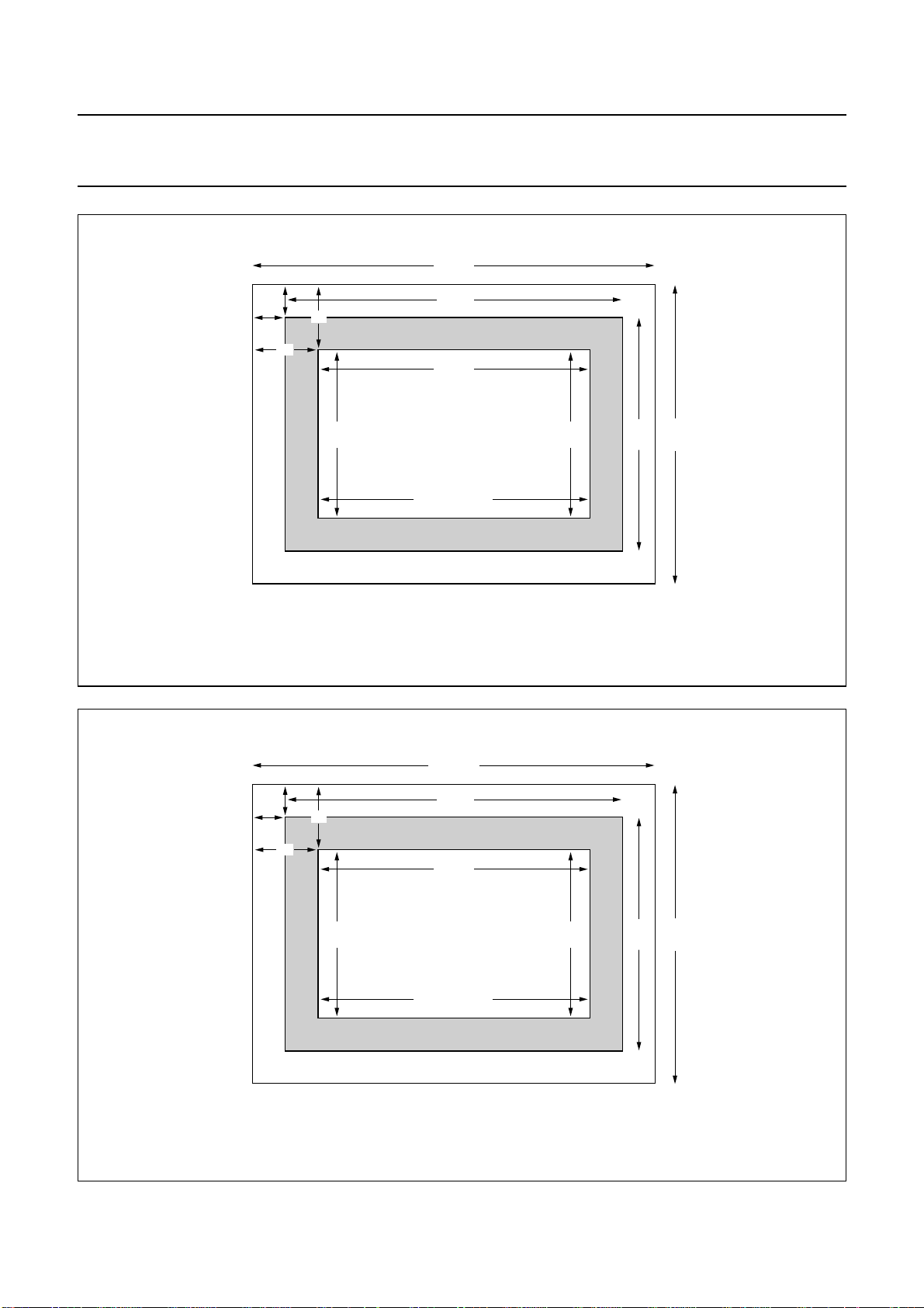
The display area starts 17.2 µs into the line and lasts for
40 µs. The display area will be in the centre of the screen
if the HSync pulse is aligned with line flyback signal.
Therefore, it is better to derive HSync directly from the line
flyback or from an output of the line output transformer
than from, say, slicing the sandcastle signal as this would
introduce delays which would shift the display to the right.
The display synchronises to the device’s HSync and
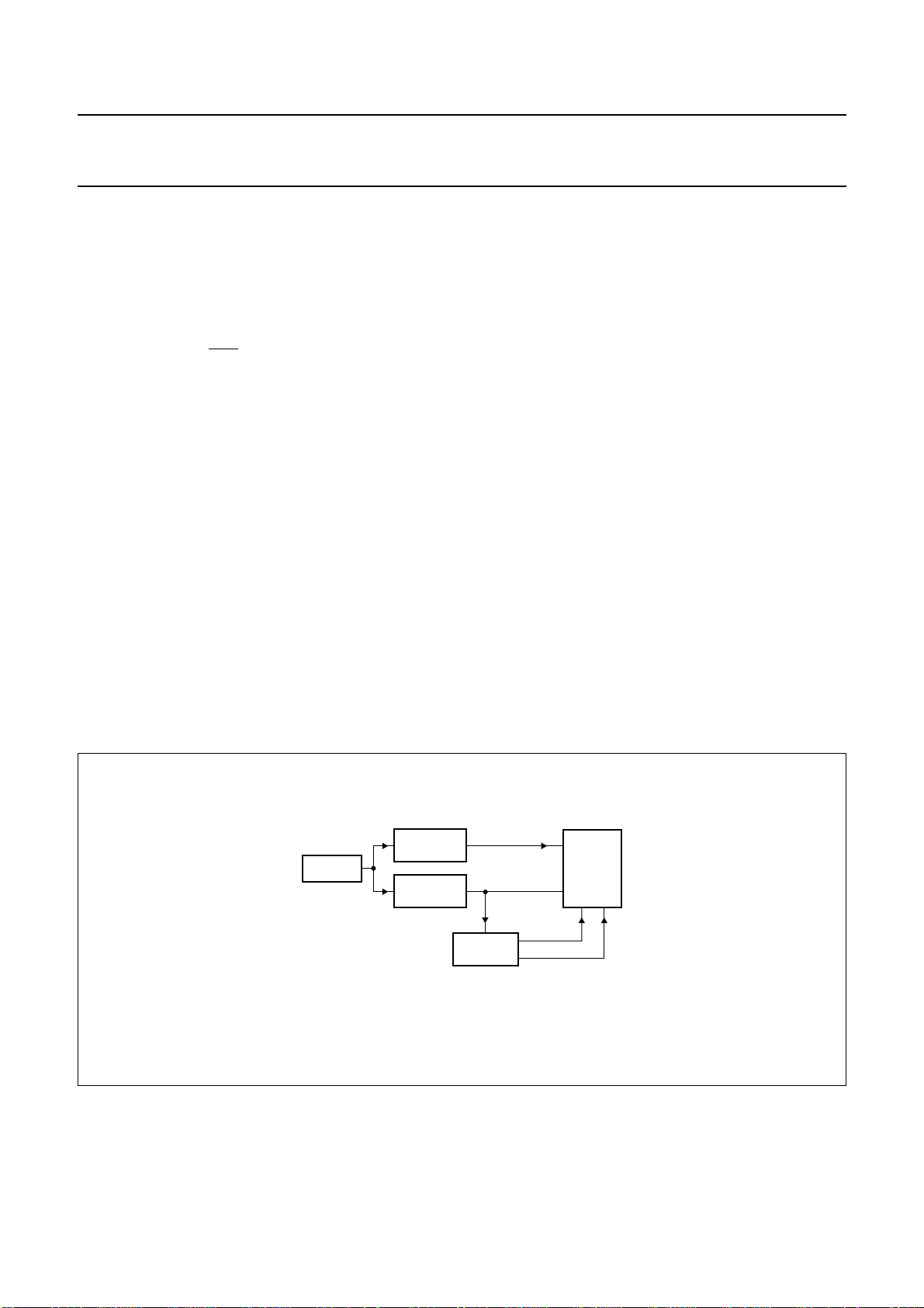
VSync inputs. A typical configuration is shown in Fig.7.
handbook, halfpage
CVBS
TUNER/IF
VIDEO
DECODING
SYNC
CIRCUITS
Fig.7 Timing configuration.
RGB
HSYNC, VSYNC
SAA5288
CRT
DISPLAY
RGB, VDS
FRAME
MGL120
1997 Jun 24 27
Page 28
Philips Semiconductors Preliminary specification
TV microcontroller with full screen
On Screen Display (OSD)
7.13 Vertical timing
The vertical display timing also resynchronizes to every
sync pulse received. This means that the device can
produce a stable display on both 625 and 525-line
screens. Display starts on the 41st line of each field and
continues for 250 lines, or until the end of the field.
Normally, television displays are interlaced, i.e. only every
other TV line is displayed on each field. It is normal to
de-interlace teletext displays to prevent the displayed
characters flickering up and down. In many TV designs this
is achieved by modulating the vertical deflection current
slightly in such a way that odd fields are shifted up and
even fields are shifted down on the screen so that
lines 1 and 314, 2 and 315 etc. are overlaid. The FRAME
output is provided to facilitate this.
If the active edge of Vsync occurs in the first half of a TV
line this is an even field and the FRAME output should be a
logic 0 for this field. Similarly, if VSync is in the second half
of the line this is an odd field and FRAME should be a
logic 1. The algorithm used to derive FRAME is such that
a consistent output will be obtained no matter where the
VSync signal is relative to the HSync signal, even if VSync
occurs at the start and mid-points of a line.
Setting the TXT0.DISABLE FRAME bit forces the FRAME
output to a logic 0. Setting the TXT0.AUTO FRAME bit
causes the FRAME output to be active when just text is
being displayed but to be forced to 0 when any video is
being displayed. This allows the de-interlacing function to
take place with virtually no software intervention.
Some TV architectures do not use the FRAME output but
accomplish the de-interlacing function in the vertical
deflection IC, under software control, by delaying the start
of the scan for one field by half a line, so that lines in this
field are moved up by one TV line. In such TVs, VSync
may occur in the first half of the line at the start of an odd
field and in the second half of the line at the start of an even
field. In order to obtain correct de-interlacing in these
circumstances, theTXT1.FIELD POLARITY must be set to
reverse the assumptions made by the vertical timing
circuits on the timing of VSync in each field. The start of the
display may be delayed by a line. The ‘Field Polarity’ bit
does not affect the FRAME output.
SAA5288
7.14 Display position
The position of the display relative to the HSync and
VSync inputs can be varied over a limited range to allow
for optimum TV set-up.
The horizontal position is controlled by the X0 and X1 bits
in SFR TXT16. Table 16 gives the time from the active
edge of the HSync signal to the start of the display area for
each setting of X0 and X1.
Table 16 Display horizontal position
X1 X0
0 0 17.2
0 1 16.2
1 0 15.2
1 1 14.2
The line on which the display area starts depends on
whether the display is 625-line or 525-line and on the
setting of the Y0 to Y2 bits in SFR TXT16. Table 17 gives
the first display line for each setting of Y0 to Y2, for both
625 and 525-line display.
On the other field, the display starts on the equivalent line.
Table 17 Display vertical position
Y2 Y1 Y0
0 0 0 42 28
0 0 1 44 30
0 1 0 46 32
0 1 1 48 34
1 0 0 34 20
1 0 1 36 22
1 1 0 38 24
1 1 1 40 26
HSYNC DISPLAY
(µs)
FIRST LINE FOR DISPLAY
625-LINE 525-LINE
1997 Jun 24 28
Page 29
Philips Semiconductors Preliminary specification
TV microcontroller with full screen
On Screen Display (OSD)
handbook, full pagewidth
23
lines
10.5
µs
∆X
∆Y
25
rows
64 µs
52 µs
40 µs
TEXT DISPLAY AREA
40 characters
TV PICTURE AREA
FIELD SCANNING AREA
250
lines
287
lines
MGL122
312
lines
SAA5288
handbook, full pagewidth
17
lines
10.5
µs
∆X
∆Y
Fig.8 625-line display format.
63.55 µs
52 µs
40 µs
25
rows
TEXT DISPLAY AREA
40 characters
TV PICTURE AREA
FIELD SCANNING AREA
225
lines
243
lines
MGL123
263
lines
Fig.9 525-line display format.
1997 Jun 24 29
Page 30
Philips Semiconductors Preliminary specification
TV microcontroller with full screen
SAA5288
On Screen Display (OSD)
7.15 Clock generator
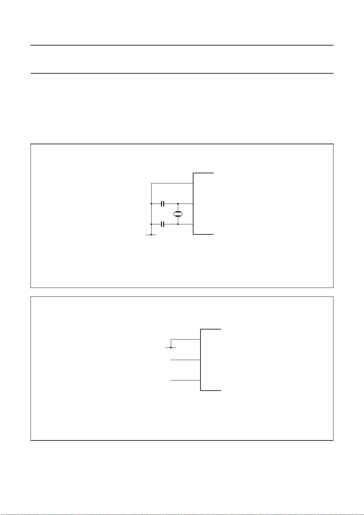
The oscillator circuit is a single-stage inverting amplifier in a Pierce oscillator configuration. The circuitry between OSCIN
and OSCOUT is basically an inverter biased to the transfer point. A crystal must be used as the feedback element to
complete the oscillator circuitry. It is operated in parallel resonance. OSCIN is the high gain amplifier input and OSCOUT
is the output.
To drive the device externally OSCIN is driven from an external source and OSCOUT is left open-circuit.
handbook, halfpage
OSCGND
(1)
C1
C2
V
SS
OSCIN
(1)
OSCOUT
MLC110
(1) The values of C1 and C2 depend on the crystal specification: C1 = C2 = 2CL.
Fig.10 Oscillator circuit.
handbook, halfpage
external clock
not connected
OSCGND
V
SS
OSCIN
OSCOUT
Fig.11 Oscillator circuit driven from external source.
MLC111
1997 Jun 24 30
Page 31
Philips Semiconductors Preliminary specification
TV microcontroller with full screen
SAA5288
On Screen Display (OSD)
8 CHARACTER SETS
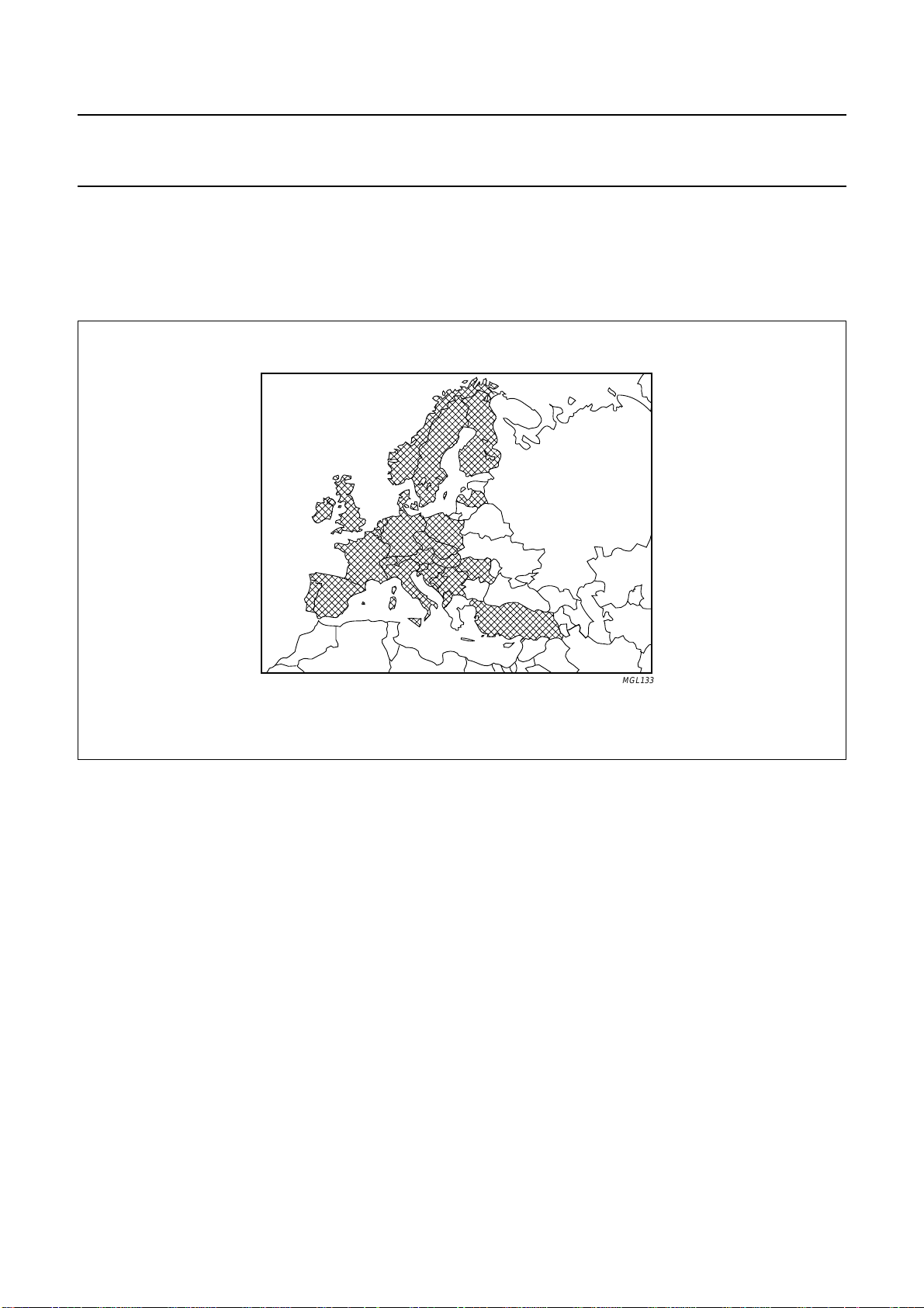
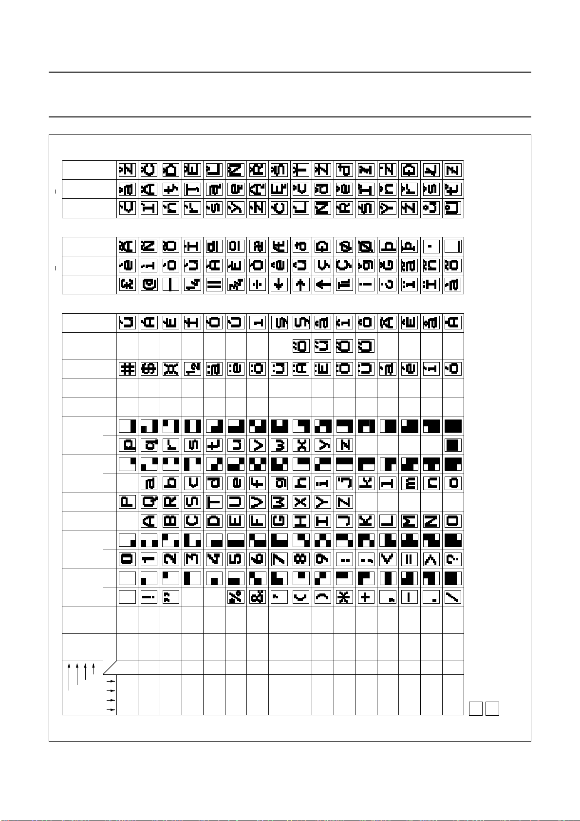
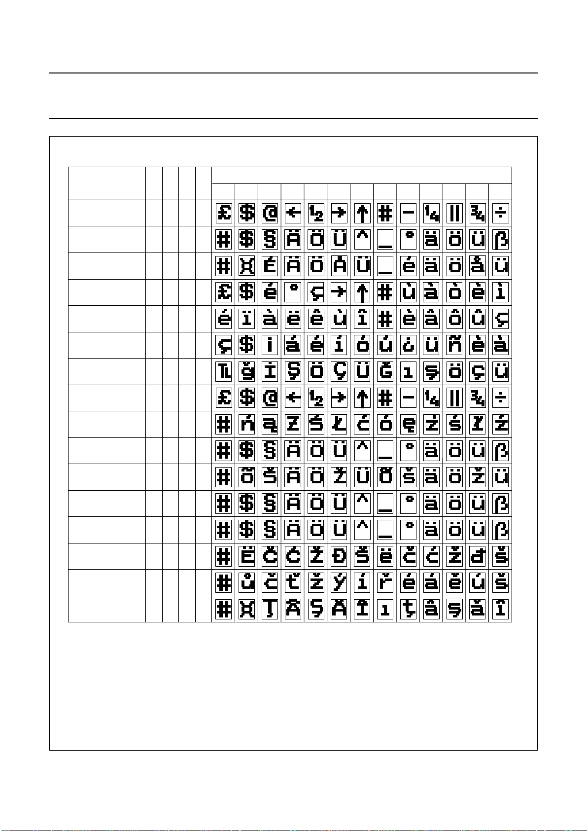
The two Pan-European character sets are shown in Figs.13 and 14. The character sets for Russian, Greek/Turkish,
Arabic/English/French, Thai and Arabic/Hebrew are available on request.
8.1 Pan-European
handbook, full pagewidth
Fig.12 Pan-European geographical coverage.
MGL133
1997 Jun 24 31
Page 32
Philips Semiconductors Preliminary specification
TV microcontroller with full screen
On Screen Display (OSD)
1
1
1
1
0
1
1
1
1
0
1
1
0
1
1
0
0
0
1
1
0
1
1
0
0
0
1
1
0
1
1
0
0
0
1
1
DEF
DEF
B
A
back-
nat
nat
black
ground
OSD
OSD
opt
opt
back
red
ground
OSDOSD
back-
green
ground
OSDOSD
back-
yellow
ground
OSDOSD
back-
ground
OSDOSD
blue
back-
ground
magenta
OSDOSD
back-
E/W = 0 E/W = 1
1
1
1
1
1
1
1
1
1
1
0
1
0
1
0
1
0
1
1
0
1
0
1
0
1
0
0
0
cyan
ground
OSDOSD
back-
white
ground
OSDOSD
OSDOSD
OSDOSD
OSDOSD
SAA5288
MGL124
size
OSD
OSD
height
double
normal
OSDOSD
OSDOSD
OSDOSD
nat
opt
nat
opt
nat
opt
nat
opt
nat
opt
nat
opt
width
double
OSDOSD
nat
nat
opt
opt
OSD
size
double
OSDOSD
nat
OSD
handbook, full pagewidth
opt
Fig.13 Pan-European basic character set.
0
1
0
0
1
0
0
0
0
0
0
0
6
b
7
b
I
T
B
0 1 22a3 3a4 5 6 6a77a8 9 C
alpha -
column
r
o
w
4
0
b
b
5
b
1
b
2
b
3
S
b
black
graphics
black
alpha -
numerics
0
0 0 0 0
red
graphics
red
numerics
10 0 0 1
green
graphics
green
alpha -
numerics
2
0 0 1 0
nat
opt
yellow
graphics
yellow
alpha -
numerics
30 0 1 1
nat
opt
blue
graphics
blue
alpha -
numerics
40 1 0 0
graphics
magenta
alpha -
magenta
numerics
5
0 1 0 1
cyan
graphics
cyan
alpha -
numerics
60 1 1 0
white
graphics
white
alpha -
numerics
70 1 1 1
1997 Jun 24 32
display
conceal
flash
8
1 0 0 0
graphics
contiguous
91 0 0 1 steady
graphics
separated
A1 0 1 0 end box
B1 0 1 1 start box
black
back -
ground
height
normal
C1 1 0 0
new
back -
ground
height
double
D1 1 0 1
hold
graphics
width
double
E1 1 1 0
release
graphics
size
double
F1 1 1 1
customer definable On-Screen Display character
character dependent on the language of page, refer to National Option characters
nat
opt
OSD
Page 33
Philips Semiconductors Preliminary specification
TV microcontroller with full screen
On Screen Display (OSD)
handbook, full pagewidth
LANGUAGE
ENGLISH
GERMAN
SWEDISH
ITALIAN
FRENCH
SPANISH
TURKISH
E/W
C12 C13 C14
(1)
(1)
(1)
(1)
(1)
(1)
(1)
0
000
0
001
0
010
0
011
0
100
10
01
1100
23
24 40
SAA5288
CHARACTER
5B 5C 5D 5E 5F 60 7B 7C 7D 7E
ENGLISH
POLISH
SERBO-CROAT
CZECH
RUMANIAN
(2)
(1)
(1)
(1)
(2)
(2)
(1)
(1)
111
0
0010
001GERMAN
1
010ESTONIAN
1
011GERMAN
1
100GERMAN
1
(1)
101
1
110
1
11
11
MGL125
(1) This language conforms to the EBU document SP492 or where superseded ETSI document pr ETS 300 706 with respect to C12/C13/C14
definition.
(2) This language is included for backward compatibility with previous generation of Philips teletext decoders.
Fig.14 National option characters.
1997 Jun 24 33
Page 34
Philips Semiconductors Preliminary specification
TV microcontroller with full screen
On Screen Display (OSD)
8.2 Russian
handbook, full pagewidth
SAA5288
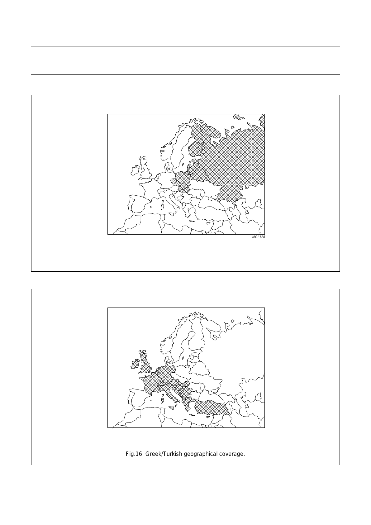
MGL128
8.3 Greek/Turkish
handbook, full pagewidth
Fig.15 Russian geographical coverage.
MGL129
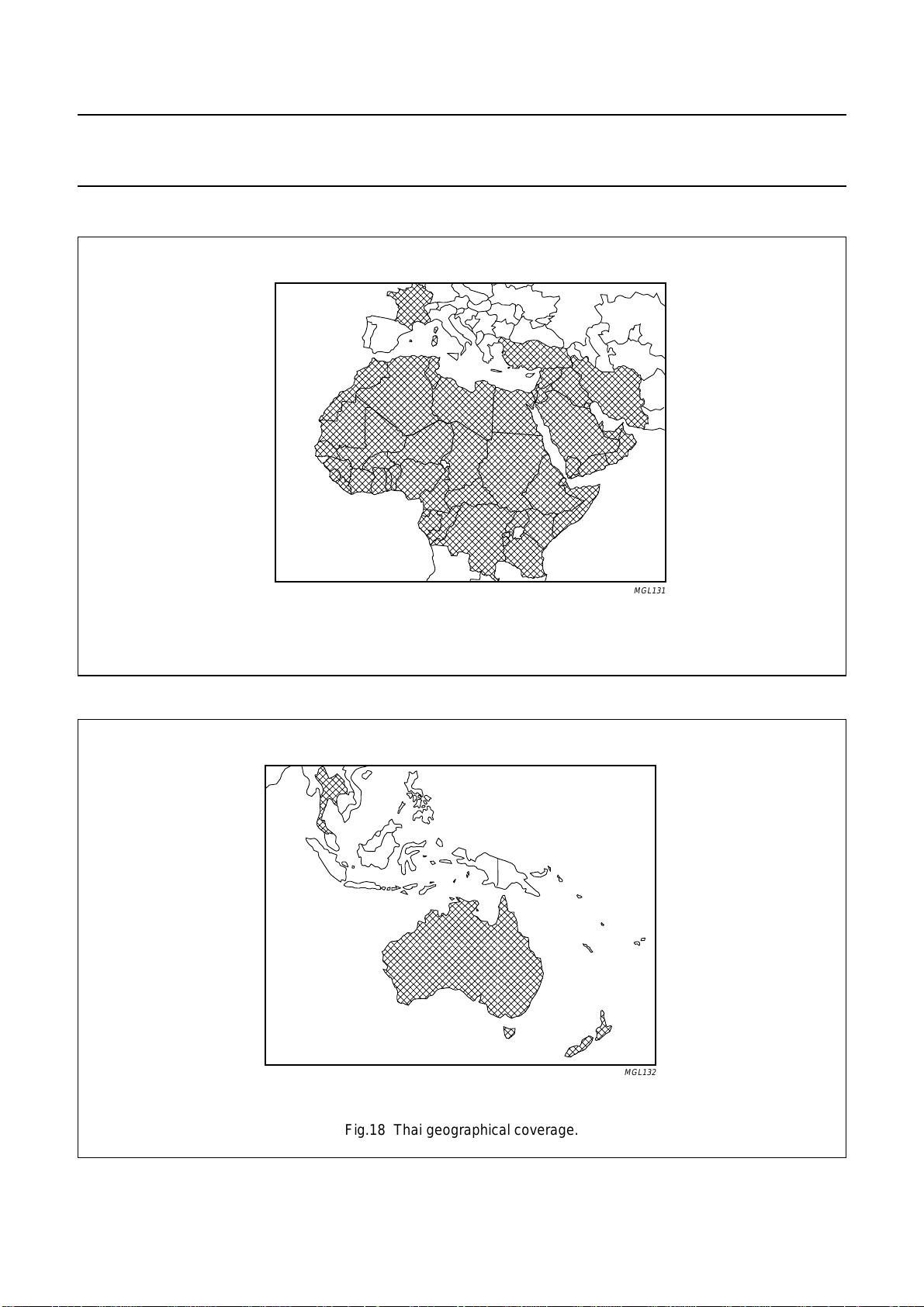
Fig.16 Greek/Turkish geographical coverage.
1997 Jun 24 34
Page 35
Philips Semiconductors Preliminary specification
,,,,,
,,,,,
,,,,,
TV microcontroller with full screen
On Screen Display (OSD)
8.4 Arabic/English/French
handbook, full pagewidth
SAA5288
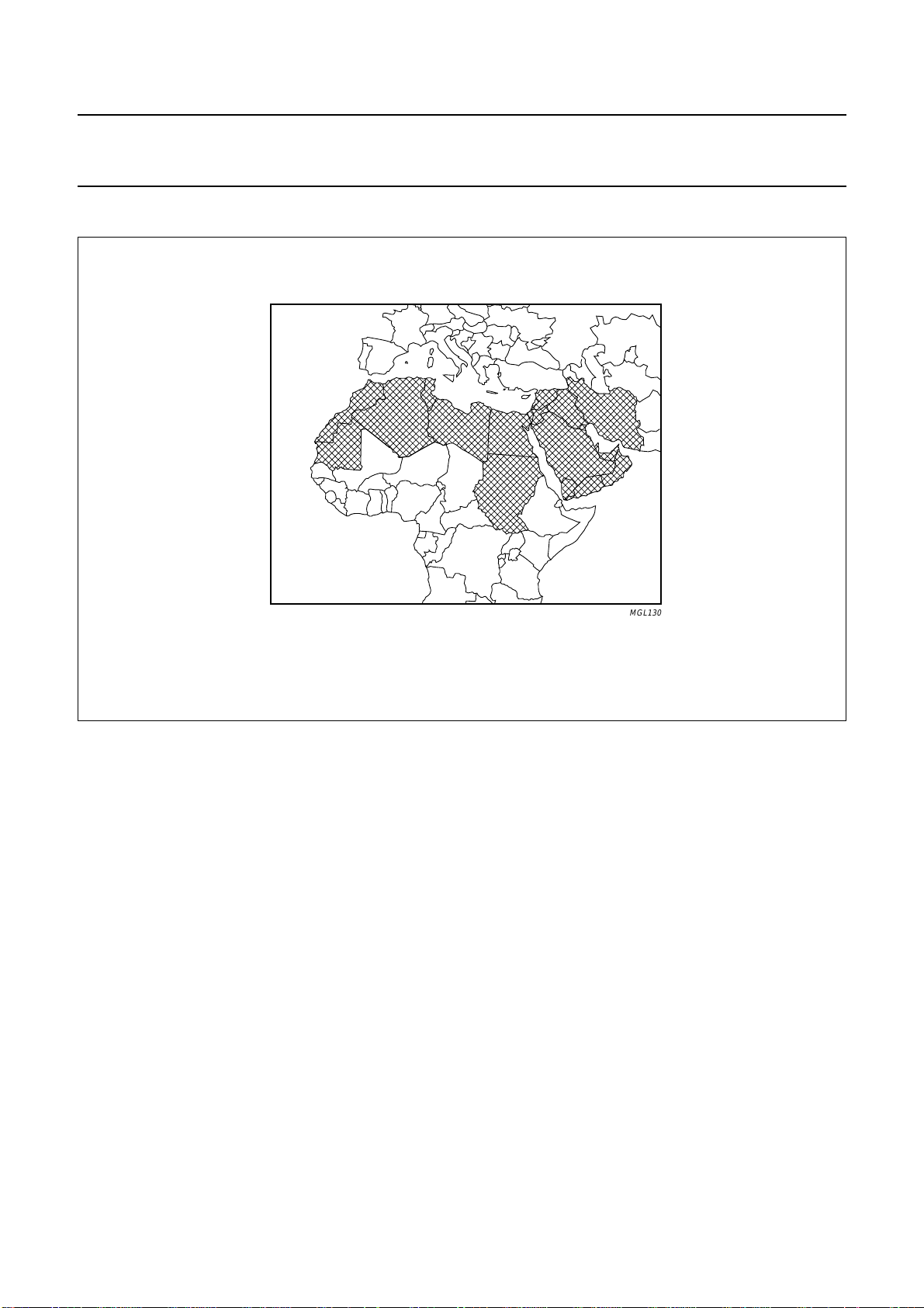
MGL131
8.5 Thai
handbook, full pagewidth
Fig.17 Arabic/English/French geographical coverage.
MGL132
1997 Jun 24 35
Fig.18 Thai geographical coverage.
Page 36
Philips Semiconductors Preliminary specification
TV microcontroller with full screen
On Screen Display (OSD)
8.6 Arabic/Hebrew
book, full pagewidth
SAA5288
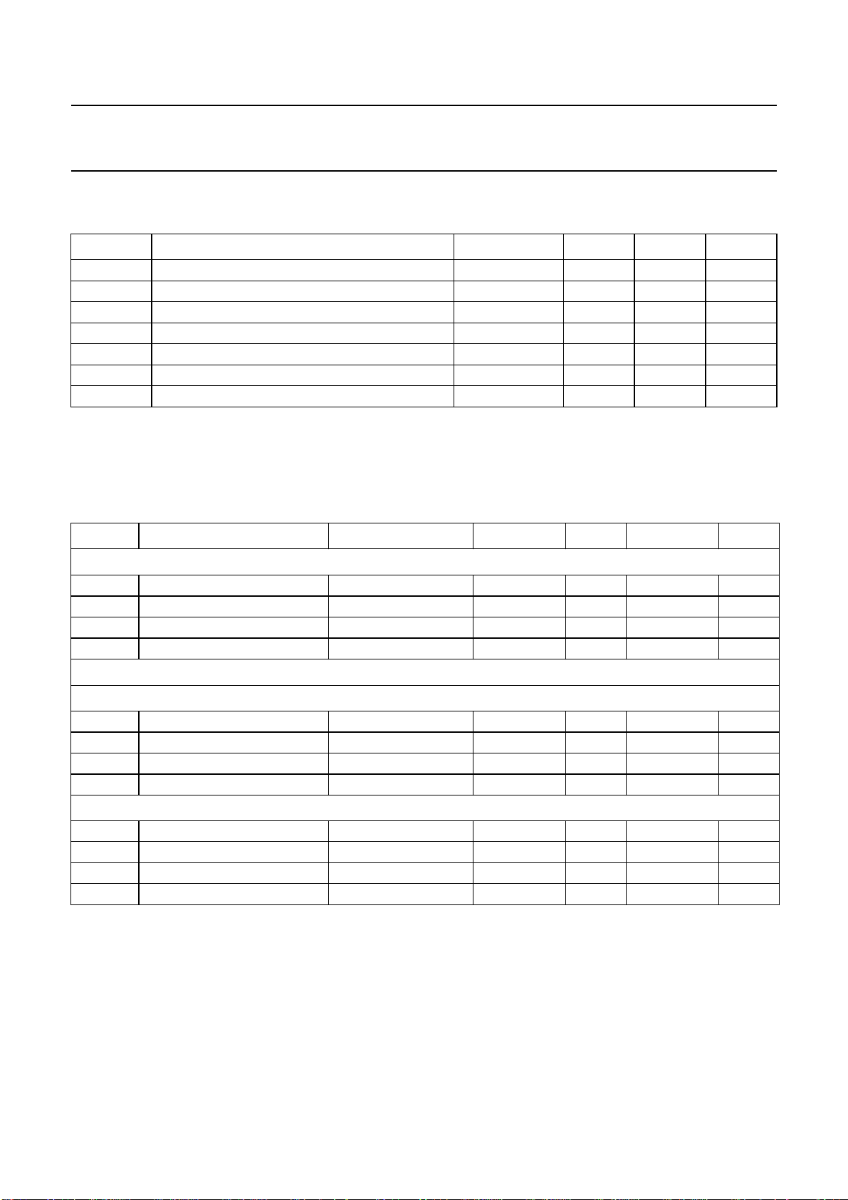
Fig.19 Arabic/Hebrew geographical coverage.
MGL130
1997 Jun 24 36
Page 37
Philips Semiconductors Preliminary specification
TV microcontroller with full screen
SAA5288
On Screen Display (OSD)
9 LIMITING VALUES
In accordance with the Absolute Maximum Rating System (IEC 134).
SYMBOL PARAMETER CONDITIONS MIN. MAX. UNIT
V
DD
V
I
V
O
I
O
I
IOK
T
amb
T
stg
Note
1. This value has an absolute maximum of 6.5 V independent of V
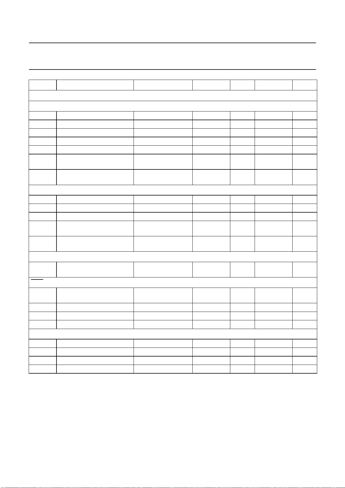
10 CHARACTERISTICS
VDD=5V±10%; VSS=0V; T
SYMBOL PARAMETER CONDITIONS MIN. TYP. MAX. UNIT
supply voltage (all supplies) −0.3 +6.5 V
input voltage (any input) note 1 −0.3 VDD+ 0.5 V
output voltage (any output) note 1 −0.3 VDD+ 0.5 V
output current (each output) −±10 mA
DC input or output diode current −±20 mA
operating ambient temperature −20 +70 °C
storage temperature −55 +125 °C
.
DD
= −20 to +70 °C; unless otherwise specified.
amb
Supplies
V
DD
I
DDM
I
DDA
I
DDT
supply voltage 4.5 5.0 5.5 V
microcontroller supply current − 15 30 mA
analog supply current − 815 mA
display supply current − 15 30 mA
Digital inputs
RESET
V
IL
V
IH
I
LI
C
I
LOW-level input voltage −0.3 − 0.2VDD− 0.1 V
HIGH-level input voltage 0.7V
input leakage current VI= 0 to V
input capacitance −−4pF
HSYNC AND VSYNC
V
th(f)
V
th(r)
V
hys
C
I
switching threshold falling 0.2V
switching threshold rising −−0.8V
hysteresis voltage − 0.33VDD− V
input capacitance −−4pF
DD
DD
− VDD+ 0.3 V
−10 − +10 µA
DD
−− V
DD
V
1997 Jun 24 37
Page 38
Philips Semiconductors Preliminary specification
TV microcontroller with full screen
SAA5288
On Screen Display (OSD)
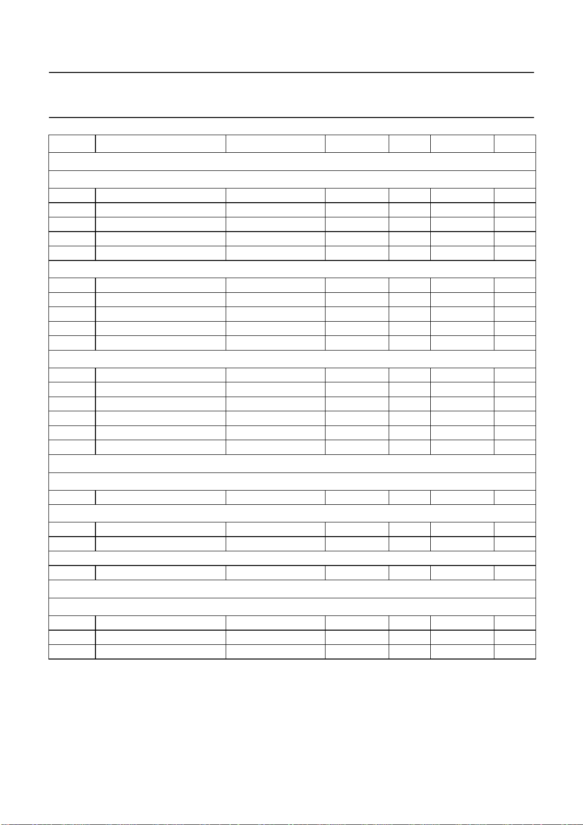
SYMBOL PARAMETER CONDITIONS MIN. TYP. MAX. UNIT
Digital outputs
R, G AND B; note 1
V
OL
V
OH
output impedance −−150 Ω
Z
O
C
L
I
O
t
r
t
f
VDS
V
OL
V
OH
C
L
t
r
t
f
R, G, B AND VDS
t
skew
COR (OPEN-DRAIN OUTPUT)
V
OH
V
OL
I
OL
C
L
FRAME
V
OH
V
OL
I
OL
C
L
LOW-level output voltage IOL= 2 mA 0 − 0.2 V
HIGH-level output voltage IOH= −2mA V
RGBREF
− 0.3 V
RGBREFVRGBREF
+ 0.4 V
load capacitance −−50 pF
DC output current −−−4mA
output rise time between 10 and 90%;
=50pF
C
L
output fall time between 90 and 10%;
−−20 ns
−−20 ns
CL=50pF
LOW-level output voltage IOL= 1.6 mA 0 − 0.2 V
HIGH-level output voltage IOH= −1.6 mA VDD− 0.3 − VDD+ 0.4 V
load capacitance −−50 pF
output rise time between 10 and 90%;
−−20 ns
CL=50pF
output fall time between 90 and 10%;
−−20 ns
CL=50pF
skew delay between any two
−−20 ns
pins
HIGH-level pull-up output
−−VDDV
voltage
LOW-level output voltage IOL= 2 mA 0 − 0.5 V
LOW-level output current −−2mA
load capacitance −−25 pF
HIGH-level output voltage IOL= 8 mA 0 − 0.5 V
LOW-level output voltage IOL= −8mA VDD− 0.5 − V
DD
V
LOW-level output current −8 − +8 mA
load capacitance −−100 pF
1997 Jun 24 38
Page 39
Philips Semiconductors Preliminary specification
TV microcontroller with full screen
SAA5288
On Screen Display (OSD)
SYMBOL PARAMETER CONDITIONS MIN. TYP. MAX. UNIT
Digital input/outputs
P0.0 TO P0.4, P0.7, P1.0 TO P1.5, P2.0 TO P2.7 AND P3.0 TO P3.4
V
IL
V
IH
C
I
V
OL
C
L
P0.5 AND P0.6
V
IL
V
IH
C
I
V
OL
C
L
P1.6 AND P1.7
V
IL
V
IH
C
I
V
OL
C
L
t
f
Analog inputs
LOW-level input voltage −0.3 − 0.2VDD− 0.1 V
HIGH-level input voltage 0.2VDD+ 0.9 − VDD+ 0.3 V
input capacitance −−4pF
LOW-level output voltage IOL= 3.2 mA 0 − 0.45 V
load capacitance −−50 pF
LOW-level input voltage −0.3 − 0.2VDD− 0.1 V
HIGH-level input voltage 0.2VDD+ 0.9 − VDD+ 0.3 V
input capacitance −−4pF
LOW-level output voltage IOL=10mA 0 − 0.45 V
load capacitance −−50 pF
LOW-level input voltage −0.3 − +1.5 V
HIGH-level input voltage 3.0 − VDD+ 0.3 V
input capacitance −−5pF
LOW-level output voltage IOL= 3 mA 0 − 0.5 V
load capacitance −−400 pF
output fall time between 3 and 1 V −−200 ns
IREF
R
gnd
resistor to ground − 27 − kΩ
RGBREF; note 1
V
I
I
I
input voltage −0.3 − V
DC input current −−12 mA
ADC0, ADC1 and ADC2
V
IL
LOW-level input voltage −0.3 − V
Crystal oscillator
OSCIN
V
IL
V
IH
C
I
LOW-level input voltage −0.3 − 0.2VDD− 0.1 V
HIGH-level input voltage 0.7V
input capacitance −−10 pF
1997 Jun 24 39
DD
DD
DD
− VDD+ 0.3 V
V
V
Page 40
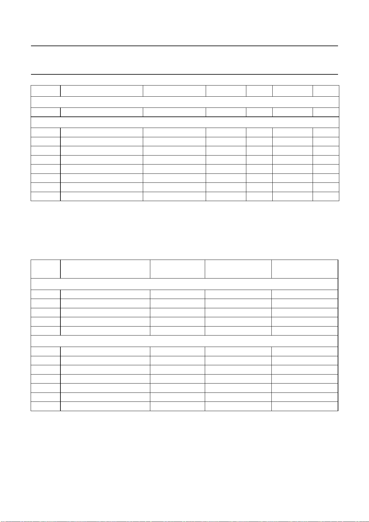
Philips Semiconductors Preliminary specification
TV microcontroller with full screen
SAA5288
On Screen Display (OSD)
SYMBOL PARAMETER CONDITIONS MIN. TYP. MAX. UNIT
OSCOUT
C
O
CRYSTAL SPECIFICATION; note 2
f
xtal
C
L
C1 series capacitance T
C0 parallel capacitance T
R
r
T
xtal
X
j
X
d
Notes
1. All RGB current is sourced from the RGBREF pin. The maximum effective series resistance between RGBREF and
the R, G and B pins is 150 Ω.
2. Crystal order number 4322 143 05561.
output capacitance −−10 pF
nominal frequency − 12 − MHz
load capacitance − 32 − pF
=25°C − 18.5 − fF
amb
=25°C − 4.9 − pF
amb
resonance resistance T
=25°C − 35 −Ω
amb
temperature range −20 +25 +70 °C
adjustment tolerance T
=25°C −−±50 × 10
amb
drift −−±30 × 10
−6
−6
2
11 CHARACTERISTICS FOR THE I
SYMBOL PARAMETER INPUT OUTPUT
C-BUS INTERFACE
I2C-BUS
SPECIFICATION
SCL timing
t
HD;STA
t
LOW
t
HIGH
t
rC
t
fC
START condition hold time ≥4.0 µs note 1 ≥4.0 µs
SCL LOW time ≥4.7 µs note 1 ≥4.7 µs
SCL HIGH time ≥4.0 µs ≥4.0 µs; note 2 ≥4.0 µs
SCL rise time ≤1.0 µs note 3 ≤1.0 µs
SCL fall time ≤0.3 µs ≤0.3 µs; note 4 ≤0.3 µs
SDA timing
t
SU;DAT1
t
HD;DAT
t
SU;STA
t
SU;STO
t
BUF
t
rD
t
fD
data set-up time ≥250 ns note 1 ≥250 ns
data hold time ≥0 ns note 1 ≥0ns
repeated START set-up time ≥4.7 µs note 1 ≥4.7 µs
STOP condition set-up time ≥4.0 µs note 1 ≥4.0 µs
bus free time ≥4.7 µs note 1 ≥4.7 µs
SDA rise time ≤1.0 µs note 3 ≤1.0 µs
SDA fall time ≤0.3 µs ≤0.3 µs; note 4 ≤0.3 µs
Notes
2
1. This parameter is determined by the user software. It must comply with the I
C-bus specification.
2. This value gives the auto-clock pulse length which meets the I2C-bus specification for the special crystal frequency.
Alternatively, the SCL pulse must be timed by software.
3. The rise time is determined by the external bus line capacitance and pull-up resistor. It must be less than 1 µs.
4. The maximum capacitance on bus lines SDA and SCL is 400 pF.
1997 Jun 24 40
Page 41
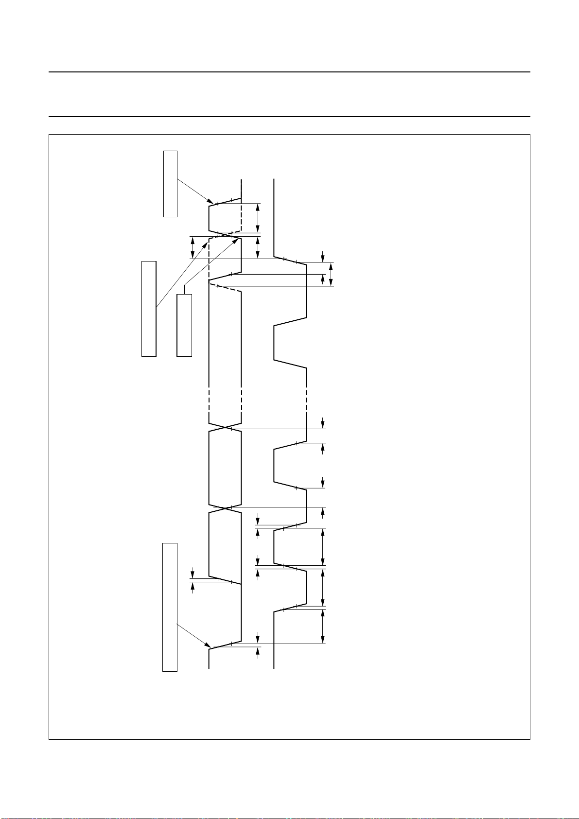
Philips Semiconductors Preliminary specification
TV microcontroller with full screen
On Screen Display (OSD)
DD
0.7VDD0.3V
START condition
BUF
t
SU;STA
t
repeated START condition
STOP condition
SU;STO
t
DD
0.7VDD0.3V
MLC104
SU;DAT3
t
SU;DAT2
t
SAA5288
fC
t
rD
t
rC
t
fD
t
START or repeated START condition
SDA
(input / output)
SCL
(input / output)
HD;DAT
t
SU;DAT1
t
HIGH
t
LOW
t
HD;STA
t
handbook, full pagewidth
C-bus interface timing.
2
Fig.20 I
1997 Jun 24 41
Page 42
Philips Semiconductors Preliminary specification
TV microcontroller with full screen
On Screen Display (OSD)
12 QUALITY SPECIFICATIONS
This device will meet Philips Semiconductors General Quality Specification for Business group
Circuits SNW-FQ-611-Part E”;“Quality Reference Handbook, order number 9398 510 63011”
requirements are shown in Tables 18 to 20.
Table 18 Acceptance tests per lot; note 1
TEST REQUIREMENTS
Mechanical cumulative target: <80 ppm
Electrical cumulative target: <80 ppm
Table 19 Processability tests (by package family); note 2
TEST REQUIREMENTS
solderability <7% LTPD
mechanical <15% LTPD
solder heat resistance <15% LTPD
Table 20 Reliability tests (by process family); note 3
SAA5288
“Consumer Integrated
. The principal
TEST CONDITIONS REQUIREMENTS
operational life 168 hours at T
humidity life temperature, humidity, bias 1000 hours, 85 °C, 85% RH
(or equivalent test)
temperature cycling
performance
Table 21 Reliability tests (by device type)
TEST CONDITIONS REQUIREMENTS
ESD and latch-up ESD Human body model 100 pF, 1.5 kΩ 2000 V
Notes to Table 16 to 18
1. ppm = fraction of defective devices, in parts per million.
2. LTPD = Lot Tolerance Percent Defective.
3. FPM = fraction of devices failing at test condition, in Failures Per Million.
T
ESD Machine model 200 pF, 0 Ω 200 V
latch-up 100 mA, 1.5 × V
stg(min)
to T
= 150 °C <1000 FPM at Tj=70°C
j
stg(max)
<2000 FPM
<2000 FPM
(absolute maximum)
DD
1997 Jun 24 42
Page 43
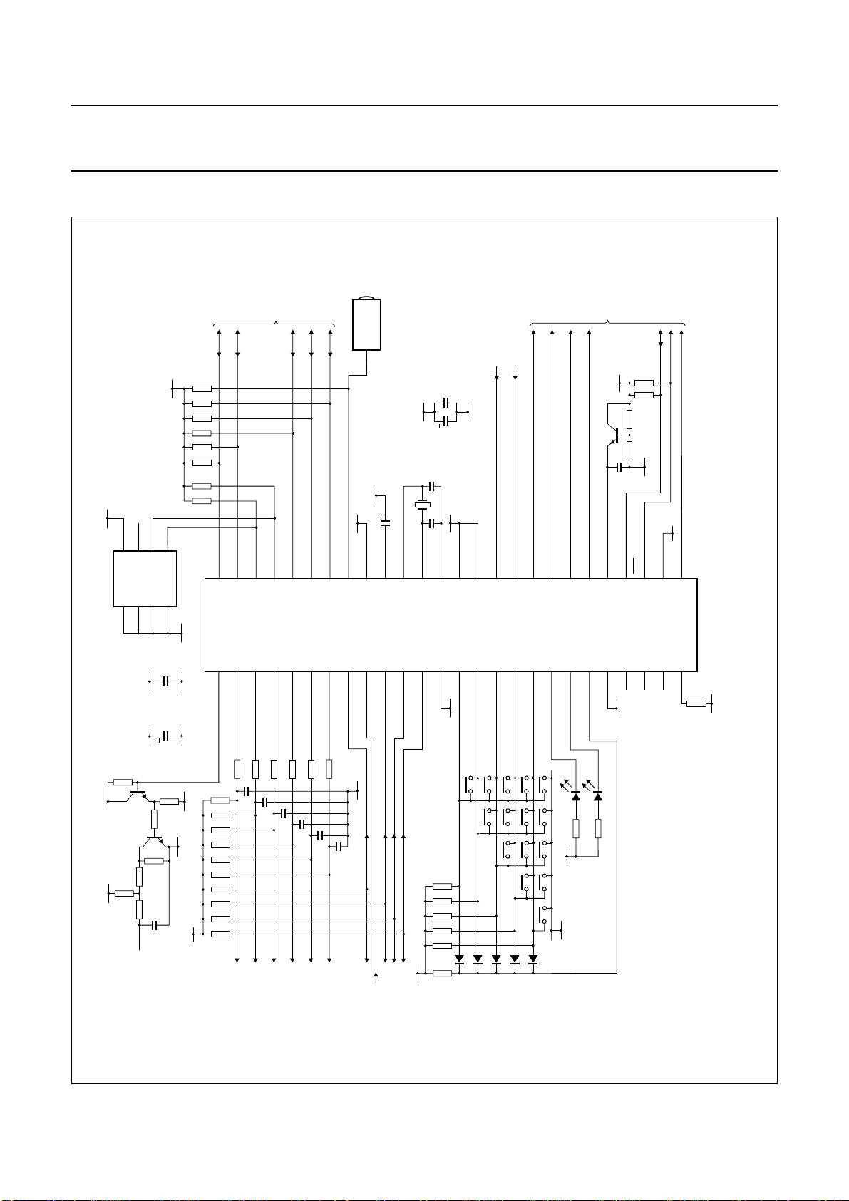
Philips Semiconductors Preliminary specification
TV microcontroller with full screen
On Screen Display (OSD)
13 APPLICATION INFORMATION
TV
control
signals
DD
V
DD
V
DD
V
dbook, full pagewidth
A0
SCL
RC
EEPROM
PCF8582E
A2
A1
DD
V
DD
V
SDA
SS
V
100 nF
47 µF
P1.4
P1.7/SDA
P1.6/SCL
P1.3/T1
P1.2/INT0
P1.5
51
50
52
SS
V
1
SS
V
SS
V
P2.1/PWM03P2.2/PWM14P2.3/PWM25P2.4/PWM36P2.5/PWM47P2.6/PWM58P2.7/PWM6
P2.0/TPWM
4948474645
2
P1.1/T0
P1.0/INT1
IR
RECEIVER
field flyback
line flyback
100 nF
47 µF
22 pF
OSCGND
SS
V
DD
V
DDDVDDA
V
VSYNC
HSYNC
VDS
R
G
B
DD
V
DD
V
DD
V
DDM
V
444342414039383736353433323130
2.2 µF
RESET
12 MHz
XTALOUT
XTALIN
SAA5288
9
P3.0/ADC0
P3.1/ADC1
SS
V
101112
P3.2/ADC2
13
SSD
V
P3.3/ADC3
14151617181920
P0.0
P0.1
P0.2
P0.3
P0.4
SS
V
P0.5
P0.6
21
P0.7
to TV's
display
circuits
DD
V
V
P3.4/PWM7
COR
RGBREF
292728
2223242625
i.c.
i.c.
SSD
V
SS
V
SAA5288
SS
SS
V
SSD
V
i.c.
IREF FRAME
MGL126
27 kΩ
SS
V
Fig.21 Application diagram.
DD
V
40 V
PH2369
tune
V
SS
V
SS
V
DD
V
hue
contrast
saturation
brightness
volume (L)
volume (R)
V
AFC
1997 Jun 24 43
1 kΩ
DD
V
SS
V
DD
V
Page 44
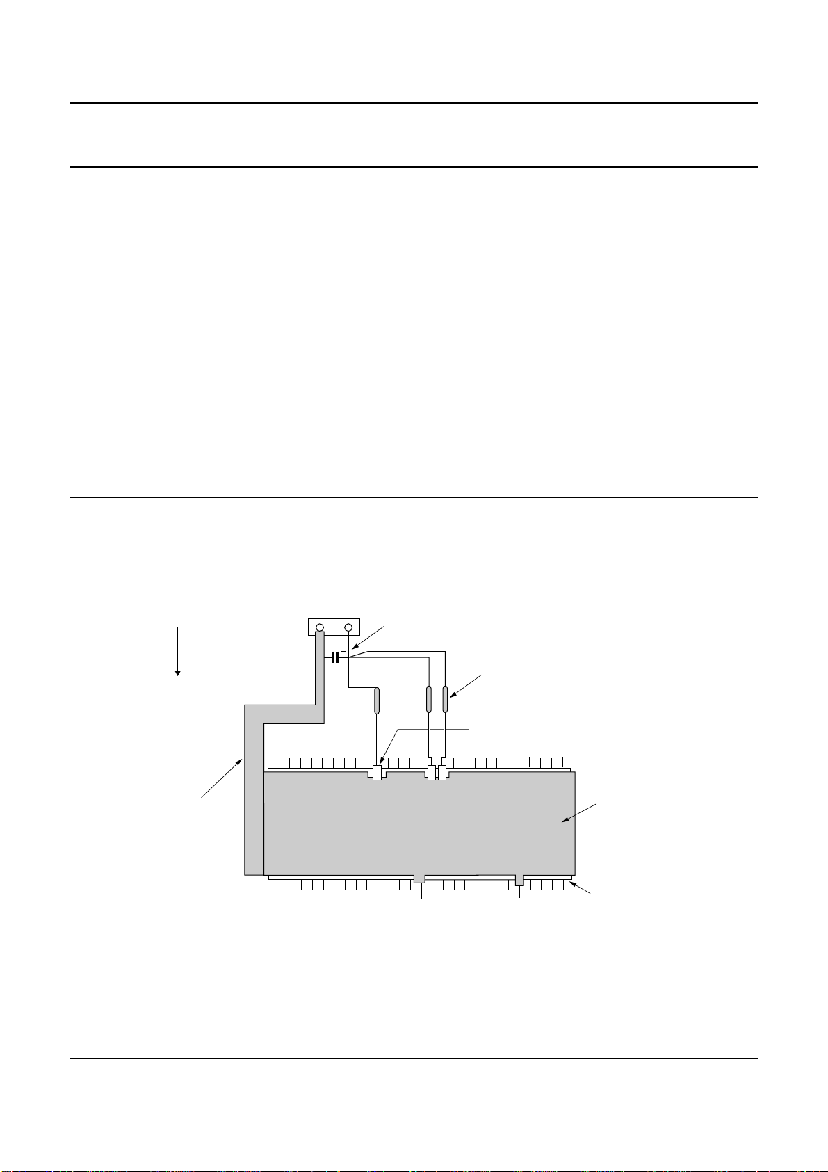
Philips Semiconductors Preliminary specification
TV microcontroller with full screen
On Screen Display (OSD)
14 EMC GUIDELINES
If possible, a ground plane under the whole IC should be
present, i.e. no signal tracks running underneath the IC as
shown in Fig.22.
The ground plane under the IC should be connected by the
widest possible connection back to the ground connection
of the PCB, and electrolytic decoupling capacitor. It should
preferably not connect to other grounds on the way and no
wire links should be present in this connection. The use of
wire links increases ground bounce by introducing
inductance into the ground, thereby reducing the
electrolytic capacitor’s decoupling efficiency.
The supply pins should be decoupled at the pin, to the
ground plane under the IC. This is easily accomplished
when using SM capacitors (which are also most effective
at high frequencies).
SAA5288
Each supply pin should be connected separately to the
power connection of the PCB, preferably via at least one
wire link which:
1. May be replaced by a ferrite or inductor at a later point
if necessary
2. Will introduce a small amount of inductance.
Signals connected to the +5 V supply e.g. via pull-up
resistors, should be connected to the +5 V supply before
the wire link to the IC (i.e. not the IC side). This will prevent
if from being polluted and conduct or radiate noise onto
signal lines, which may then radiate themselves.
OSCGND should connect only to the crystal load
capacitors (and not GND).
handbook, full pagewidth
under-IC GND plane
GND connection
note: no wire links
other
GND
connections
GND
+5 V
V
electrolytic decoupling capacitor (2 µF)
SM decoupling capacitors (10 to 100 nF)
SSD
V
DDA
DDM
V
DDD
V
wire links
V
SSA
under-IC GND plane
IC
MGL127
Fig.22 Power supply and GND connections for SOT247-1.
1997 Jun 24 44
Page 45
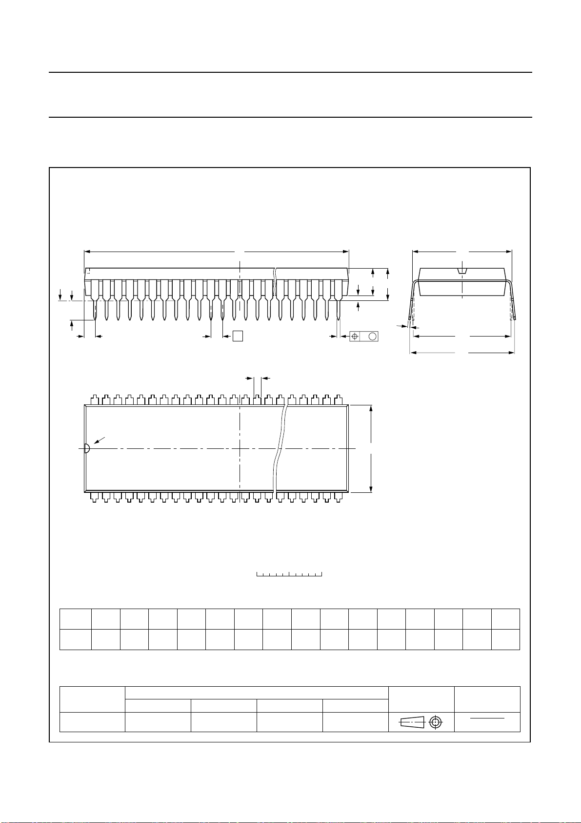
Philips Semiconductors Preliminary specification
TV microcontroller with full screen
On Screen Display (OSD)
15 PACKAGE OUTLINE
SDIP52: plastic shrink dual in-line package; 52 leads (600 mil)
D
seating plane
L
Z
e
SAA5288
SOT247-1
M
E
A
2
A
A
1
w M
b
1
c
(e )
M
1
H
52
pin 1 index
1
DIMENSIONS (mm are the original dimensions)
A
A
A
UNIT b
mm
max.
5.08 0.51 4.0
12
min.
max.
b
1.3
0.8
0.53
0.40
b
27
E
26
0 5 10 mm
scale
cEe M
1
0.32
0.23
(1) (1)
D
47.9
47.1
14.0
13.7
1
L
M
E
3.2
15.80
2.8
15.24
17.15
15.90
e
w
H
0.181.778 15.24
Z
max.
1.73
(1)
Note
1. Plastic or metal protrusions of 0.25 mm maximum per side are not included.
OUTLINE
VERSION
SOT247-1
IEC JEDEC EIAJ
REFERENCES
1997 Jun 24 45
EUROPEAN
PROJECTION
ISSUE DATE
90-01-22
95-03-11
Page 46

Philips Semiconductors Preliminary specification
TV microcontroller with full screen
On Screen Display (OSD)
16 SOLDERING
16.1 Introduction
There is no soldering method that is ideal for all IC
packages. Wave soldering is often preferred when
through-hole and surface mounted components are mixed
on one printed-circuit board. However, wave soldering is
not always suitable for surface mounted ICs, or for
printed-circuits with high population densities. In these
situations reflow soldering is often used.
This text gives a very brief insight to a complex technology.
A more in-depth account of soldering ICs can be found in
our
“IC Package Databook”
16.2 Soldering by dipping or by wave
The maximum permissible temperature of the solder is
260 °C; solder at this temperature must not be in contact
with the joint for more than 5 seconds. The total contact
time of successive solder waves must not exceed
5 seconds.
(order code 9398 652 90011).
SAA5288
The device may be mounted up to the seating plane, but
the temperature of the plastic body must not exceed the
specified maximum storage temperature (T
printed-circuit board has been pre-heated, forced cooling
may be necessary immediately after soldering to keep the
temperature within the permissible limit.
16.3 Repairing soldered joints
Apply a low voltage soldering iron (less than 24 V) to the
lead(s) of the package, below the seating plane or not
more than 2 mm above it. If the temperature of the
soldering iron bit is less than 300 °C it may remain in
contact for up to 10 seconds. If the bit temperature is
between 300 and 400 °C, contact may be up to 5 seconds.
stg max
). If the
1997 Jun 24 46
Page 47
Philips Semiconductors Preliminary specification
TV microcontroller with full screen
SAA5288
On Screen Display (OSD)
17 DEFINITIONS
Data sheet status
Objective specification This data sheet contains target or goal specifications for product development.
Preliminary specification This data sheet contains preliminary data; supplementary data may be published later.
Product specification This data sheet contains final product specifications.
Limiting values
Limiting values given are in accordance with the Absolute Maximum Rating System (IEC 134). Stress above one or
more of the limiting values may cause permanent damage to the device. These are stress ratings only and operation
of the device at these or at any other conditions above those given in the Characteristics sections of the specification
is not implied. Exposure to limiting values for extended periods may affect device reliability.
Application information
Where application information is given, it is advisory and does not form part of the specification.
18 LIFE SUPPORT APPLICATIONS
These products are not designed for use in life support appliances, devices, or systems where malfunction of these
products can reasonably be expected to result in personal injury. Philips customers using or selling these products for
use in such applications do so at their own risk and agree to fully indemnify Philips for any damages resulting from such
improper use or sale.
19 PURCHASE OF PHILIPS I
Purchase of Philips I
components in the I2C system provided the system conforms to the I2C specification defined by
Philips. This specification can be ordered using the code 9398 393 40011.
2
C COMPONENTS
2
C components conveys a license under the Philips’ I2C patent to use the
1997 Jun 24 47
Page 48

Philips Semiconductors – a worldwide company
Argentina: see South America
Australia: 34 Waterloo Road, NORTH RYDE, NSW 2113,
Tel. +61 2 9805 4455, Fax. +61 2 9805 4466
Austria: Computerstr. 6, A-1101 WIEN, P.O. Box 213,
Tel. +43 1 60 101, Fax. +43 1 60 101 1210
Belarus: Hotel Minsk Business Center, Bld. 3, r. 1211, Volodarski Str. 6,
220050 MINSK, Tel. +375 172 200 733, Fax. +375 172 200 773
Belgium: see The Netherlands
Brazil: see South America
Bulgaria: Philips Bulgaria Ltd., Energoproject, 15th floor,
51 James Bourchier Blvd., 1407 SOFIA,
Tel. +359 2 689 211, Fax. +359 2 689 102
Canada: PHILIPS SEMICONDUCTORS/COMPONENTS,
Tel. +1 800 234 7381
China/Hong Kong: 501 Hong Kong Industrial Technology Centre,
72 Tat Chee Avenue, Kowloon Tong, HONG KONG,
Tel. +852 2319 7888, Fax. +852 2319 7700
Colombia: see South America
Czech Republic: see Austria
Denmark: Prags Boulevard 80, PB 1919, DK-2300 COPENHAGEN S,
Tel. +45 32 88 2636, Fax. +45 31 57 0044
Finland: Sinikalliontie 3, FIN-02630 ESPOO,
Tel. +358 9 615800, Fax. +358 9 61580920
France: 4 Rue du Port-aux-Vins, BP317, 92156 SURESNES Cedex,
Tel. +33 1 40 99 6161, Fax. +33 1 40 99 6427
Germany: Hammerbrookstraße 69, D-20097 HAMBURG,
Tel. +49 40 23 53 60, Fax. +49 40 23 536 300
Greece: No. 15, 25th March Street, GR 17778 TAVROS/ATHENS,
Tel. +30 1 4894 339/239, Fax. +30 1 4814 240
Hungary: see Austria
India: Philips INDIA Ltd, Shivsagar Estate, A Block, Dr. Annie Besant Rd.
Worli, MUMBAI 400 018, Tel. +91 22 4938 541, Fax. +91 22 4938 722
Indonesia: see Singapore
Ireland: Newstead, Clonskeagh, DUBLIN 14,
Tel. +353 1 7640 000, Fax. +353 1 7640 200
Israel: RAPAC Electronics, 7 Kehilat Saloniki St, PO Box 18053,
TEL AVIV 61180, Tel. +972 3 645 0444, Fax. +972 3 649 1007
Italy: PHILIPS SEMICONDUCTORS, Piazza IV Novembre 3,
20124 MILANO, Tel. +39 2 6752 2531, Fax. +39 2 6752 2557
Japan: Philips Bldg 13-37, Kohnan 2-chome, Minato-ku, TOKYO 108,
Tel. +81 3 3740 5130, Fax. +81 3 3740 5077
Korea: Philips House, 260-199 Itaewon-dong, Yongsan-ku, SEOUL,
Tel. +82 2 709 1412, Fax. +82 2 709 1415
Malaysia: No. 76 Jalan Universiti, 46200 PETALING JAYA, SELANGOR,
Tel. +60 3 750 5214, Fax. +60 3 757 4880
Mexico: 5900 Gateway East, Suite 200, EL PASO, TEXAS 79905,
Tel. +9-5 800 234 7381
Middle East: see Italy
Netherlands: Postbus 90050, 5600 PB EINDHOVEN, Bldg. VB,
Tel. +31 40 27 82785, Fax. +31 40 27 88399
New Zealand: 2 Wagener Place, C.P.O. Box 1041, AUCKLAND,
Tel. +64 9 849 4160, Fax. +64 9 849 7811
Norway: Box 1, Manglerud 0612, OSLO,
Tel. +47 22 74 8000, Fax. +47 22 74 8341
Philippines: Philips Semiconductors Philippines Inc.,
106 Valero St. Salcedo Village, P.O. Box 2108 MCC, MAKATI,
Metro MANILA, Tel. +63 2 816 6380, Fax. +63 2 817 3474
Poland: Ul. Lukiska 10, PL 04-123 WARSZAWA,
Tel. +48 22 612 2831, Fax. +48 22 612 2327
Portugal: see Spain
Romania: see Italy
Russia: Philips Russia, Ul. Usatcheva 35A, 119048 MOSCOW,
Tel. +7 095 755 6918, Fax. +7 095 755 6919
Singapore: Lorong 1, Toa Payoh, SINGAPORE 1231,
Tel. +65 350 2538, Fax. +65 251 6500
Slovakia: see Austria
Slovenia: see Italy
South Africa: S.A. PHILIPS Pty Ltd., 195-215 Main Road Martindale,
2092 JOHANNESBURG, P.O. Box 7430 Johannesburg 2000,
Tel. +27 11 470 5911, Fax. +27 11 470 5494
South America: Rua do Rocio 220, 5th floor, Suite 51,
04552-903 São Paulo, SÃO PAULO - SP, Brazil,
Tel. +55 11 821 2333, Fax. +55 11 829 1849
Spain: Balmes 22, 08007 BARCELONA,
Tel. +34 3 301 6312, Fax. +34 3 301 4107
Sweden: Kottbygatan 7, Akalla, S-16485 STOCKHOLM,
Tel. +46 8 632 2000, Fax. +46 8 632 2745
Switzerland: Allmendstrasse 140, CH-8027 ZÜRICH,
Tel. +41 1 488 2686, Fax. +41 1 481 7730
Taiwan: Philips Semiconductors, 6F, No. 96, Chien Kuo N. Rd., Sec. 1,
TAIPEI, Taiwan Tel. +886 2 2134 2865, Fax. +886 2 2134 2874
Thailand: PHILIPS ELECTRONICS (THAILAND) Ltd.,
209/2 Sanpavuth-Bangna Road Prakanong, BANGKOK 10260,
Tel. +66 2 745 4090, Fax. +66 2 398 0793
Turkey: Talatpasa Cad. No. 5, 80640 GÜLTEPE/ISTANBUL,
Tel. +90 212 279 2770, Fax. +90 212 282 6707
Ukraine: PHILIPS UKRAINE, 4 Patrice Lumumba str., Building B, Floor 7,
252042 KIEV, Tel. +380 44 264 2776, Fax. +380 44 268 0461
United Kingdom: Philips Semiconductors Ltd., 276 Bath Road, Hayes,
MIDDLESEX UB3 5BX, Tel. +44 181 730 5000, Fax. +44 181 754 8421
United States: 811 East Arques Avenue, SUNNYVALE, CA 94088-3409,
Tel. +1 800 234 7381
Uruguay: see South America
Vietnam: see Singapore
Yugoslavia: PHILIPS, Trg N. Pasica 5/v, 11000 BEOGRAD,
Tel. +381 11 625 344, Fax.+381 11 635 777
For all other countries apply to: Philips Semiconductors, Marketing & Sales Communications,
Building BE-p, P.O. Box 218, 5600 MD EINDHOVEN, The Netherlands, Fax. +31 40 27 24825
© Philips Electronics N.V. 1997 SCA54
All rights are reserved. Reproduction in whole or in part is prohibited without the prior written consent of the copyright owner.
The information presented in this document does not form part of any quotation or contract, is believed to be accurate and reliable and may be changed
without notice. No liability will be accepted by the publisher for any consequence of its use. Publication thereof does not convey nor imply any license
under patent- or other industrial or intellectual property rights.
Internet: http://www.semiconductors.philips.com
Printed in The Netherlands 547047/00/01/pp48 Date of release: 1997 Jun 24 Document order number: 9397 750 01856
 Loading...