

Page 1

INTEGRATED CIRCUITS
DATA SH EET
SAA5290
One page Economy Teletext/TV
microcontroller
Preliminary specification
File under Integrated Circuits, IC02
Philips Semiconductors
February 1995
Page 2

Philips Semiconductors Preliminary specification
One page Economy Teletext/TV
microcontroller
FEATURES
General
• Complete one page teletext decoder and TV
microcontroller in a single 52-pin package
• Eastern European, Western European and Turkish
language variants covered in one device
• Double size, double width and double height character
capability for On-Screen Display (OSD)
• Enhanced display features including meshing and
shadowing
• Separate display and acquisition timing for increased
flexibility
• Minimum peripheral component count
• 525 line and 625 line display synchronization
• Standby mode through power-down of teletext and
analog hardware.
Microcontroller
• 16 kbytes masked ROM (16 kbytes EEPROM variant for
product development)
• 256 bytes of on-chip RAM
• Six 6-bit Pulse Width Modulators (PWM) and one 14-bit
precision PWM
• 4-bit Digital-to-Analog Converter (DAC) and comparator
with a 3-input multiplexer allowing implementation of 3
Analog-to-Digital Converters (ADC) in software
• 2 high current (10 mA) open-drain outputs
• Interrupt logic 0 triggered on rising and falling edges,
providing pulse-width measurement for remote control
decoding
2
• Master and slave bit-level I
C-bus hardware.
SAA5290
DESCRIPTION
The SAA5290 is a single-chip one page teletext decoder
and television control microcontroller. The device will
decode 625-line based World System Teletext
transmissions and provides television control functions
and On-Screen Display (OSD) functions.
The teletext decoder hardware is a derivative of the
SAA5254 (IVT1.1X), and the TV control functionality
provided by an on-chip industrial standard 80C51
microcontroller. A single-page static RAM is included
on-board providing a complete one page teletext decoder
and OSD memory.
The SAA5290 is available as a mask-programmed ROM
version. An EEPROM version is also available for product
development. Both versions are available in an SDIP52
package.
ORDERING INFORMATION
TYPE NUMBER MEMORY
SAA5290ZP/nnn
SAA5290ZP/NVI
Notes
1. nnn is a three-digit number referencing the microcontroller program ROM mask.
2. I is a digit number referring to the language variant of the SAA5290ZP/NV.
February 1995 2
(1)
(2)
ROM SDIP52 plastic shrink dual in-line package; 52 leads (600 mil) SOT247-1
EEPROM SDIP52 plastic shrink dual in-line package; 52 leads (600 mil) SOT247-1
NAME DESCRIPTION VERSION
PACKAGE
Page 3
Philips Semiconductors Preliminary specification
One page Economy Teletext/TV
SAA5290
microcontroller
QUICK REFERENCE DATA
SYMBOL PARAMETER MIN. TYP. MAX. UNIT
V
DD
I
DDM
I
DDA
I
DDT
f
xtal
T
amb
BLOCK DIAGRAM
handbook, full pagewidth
2
CVBS0
CVBS1
23, 24
supply voltage 4.5 5.0 5.5 V
microcontroller supply current − 25 40 mA
analog supply current − 35 50 mA
teletext supply current − 20 30 mA
crystal frequency − 12 − MHz
operating ambient temperature −20 − +70 °C
BLACK IREF
25
DATA SLICER
V
V
DDA
26
TELETEXT
ACQUISITION
38
DDT
V
DDM
44
39
DISPLAY
TIMING
37
VSYNC
36
HSYNC
27
FRAME
OSCIN
OSCOUT
OSCGND
RESET
41
42
40
43
V
SSD1
ACQUISITION
TIMING
OSCILLATOR
80C51
MICRO-
CONTROLLER
2813
SSD2
V
V
data
address
22
SSA
ADC0 to ADC2
SAA5290
16K x 8
ANALOG-TOCONVERTER
PORT 3
5
9 to 12, 30
P3.0 to P3.4/
ROM
DIGITAL
PAGE
RAM
256 x 8
MODULATOR
PORT 2
8
1 to 8
P2.0 to P2.7
PWM
RAM
PULSE
WIDTH
P1.0 to P1.7 / INT0,
INT1, T0, T1, SDA, SCL
INTERFACE
PORT 1
8
45 to 52
DISPLAY
TEXT
TIMER/
CTRS/ I C
2
3
34, 33, 32
PORT 0
8
14 to 21
P0.0 to P0.7
R, G, B
35
VDS
29
COR
31
RGBREF
MLC102
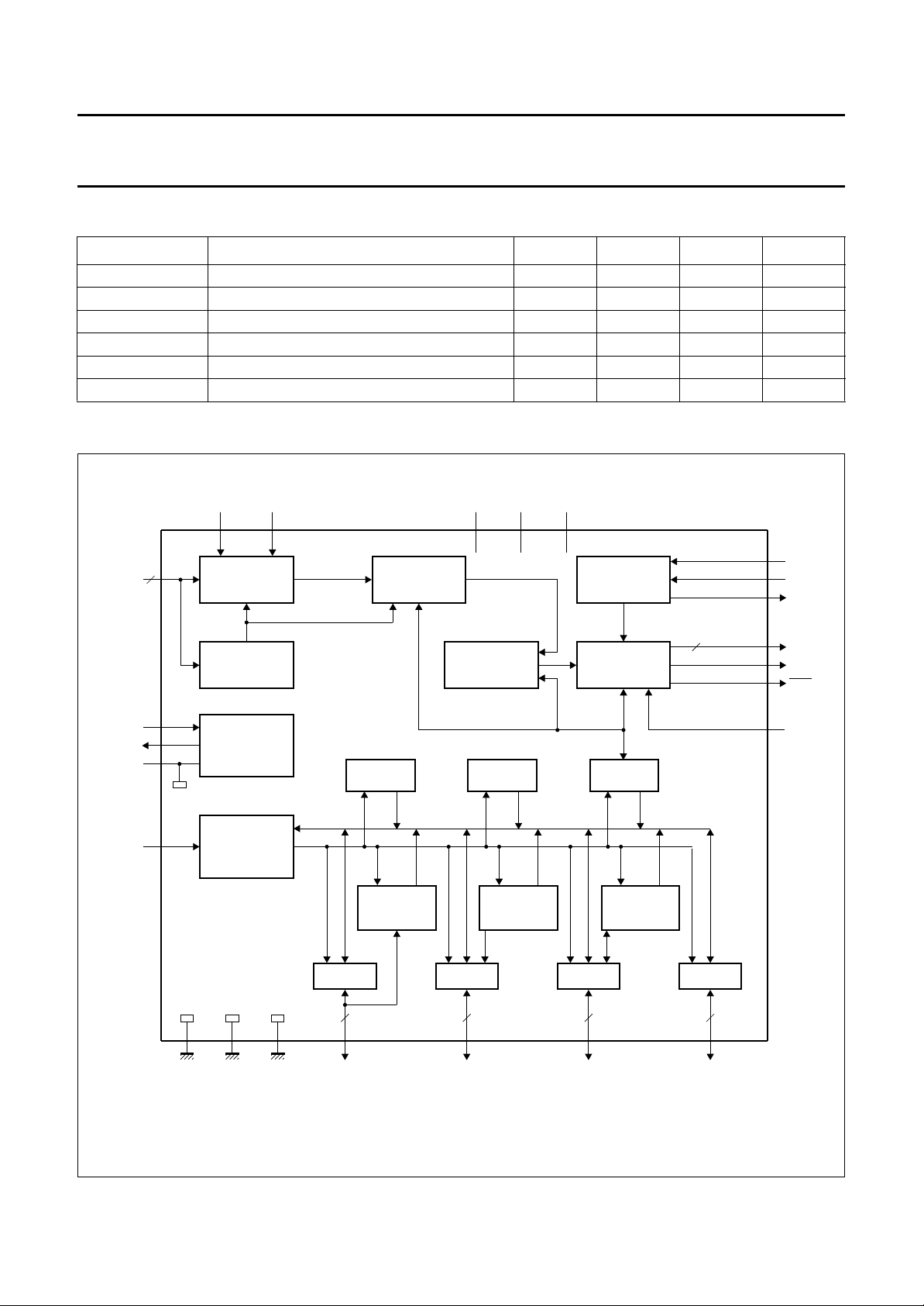
Fig.1 Block diagram.
February 1995 3
Page 4

Philips Semiconductors Preliminary specification
One page Economy Teletext/TV
SAA5290
microcontroller
PINNING
SYMBOL PIN DESCRIPTION
P2.0/TPWM 1 PORT 2: 8-bit open-drain bidirectional port with alternative functions. P2.0/TPWM is the
P2.1/PWM0 2
P2.2/PWM1 3
P2.3/PWM2 4
P2.4/PWM3 5
P2.5/PWM4 6
P2.6/PWM5 7
P2.7 8
P3.0/ADC0 9 PORT 3: 5-bit open-drain bidirectional port with alternative functions. P3.0/ADC0 to
P3.1/ADC1 10
P3.2/ADC2 11
P3.3 12
P3.4 30
V
SSD1
P0.0 14 PORT 0: 8-bit open-drain bidirectional port. P0.5 and P0.6 have 10 mA current sinking
P0.1 15
P0.2 16
P0.3 17
P0.4 18
P0.5 19
P0.6 20
P0.7 21
V
SSA
CVBS0 23 Composite video input. A positive-going 1 V (peak-to-peak) input is required, connected
CVBS1 24
BLACK 25 Video black level storage input. This pin should be connected to V
IREF 26 Reference current input for analog circuits, connected to V
FRAME 27 De-interlace output synchronized with the VSYNC pulse to produce a non-interlaced
V
SSD2
COR 29 Open-drain, active LOW output which allows selective contrast reduction of the TV
RGBREF 31 DC input voltage to define the output HIGH level on the RGB pins.
B 32 Dot rate character output of the BLUE colour information.
G 33 Dot rate character output of the GREEN colour information.
R 34 Dot rate character output of the RED colour information.
VDS 35 Video/data switch push-pull output for dot rate fast blanking.
HSYNC 36 Horizontal sync dedicated input for a TTL-level version of the horizontal sync pulse. The
13 digital ground 1 for teletext and microcontroller circuits.
22 analog ground.
28 Digital ground 2.
output for the 14-bit high precision PWM. P2.1/PWM0 to P2.6/PWM5 are the outputs for
the 6-bit PWMs 0 to 5.
P3.2/ADC2 are the inputs for the software ADC facility.
capability at 0.5 V for direct drive of LEDs.
via a 100 nF capacitor.
via a 100 nF
SSA
capacitor.
via a 27 kΩ resistor.
SSA
display by adjustment of the vertical deflection currents.
picture to enhance a mixed mode display.
polarity of this pulse is programmable by register bit TXT1.H POLARITY.
February 1995 4
Page 5

Philips Semiconductors Preliminary specification
One page Economy Teletext/TV
SAA5290
microcontroller
SYMBOL PIN DESCRIPTION
VSYNC 37 Vertical sync dedicated input for a TTL-level version of the vertical sync pulse. The
polarity of this pulse is programmable by register bit TXT1.V POLARITY.
V
DDA
V
DDT
OSCGND 40 Crystal oscillator ground.
OSCIN 41 12 MHz crystal oscillator input.
OSCOUT 42 12 MHz crystal oscillator output.
RESET 43 If the reset input is HIGH for 2 machine cycles (24 oscillator periods) while the oscillator
V
DDM
P1.0/INT1 45 PORT 1: 8-bit open-drain bidirectional port with alternative functions. P1.0/INT1 is
P1.1/T0 46
P1.2/INT0 47
P1.3/T1 48
P1.6/SCL 49
P1.7/SDA 50
P1.4 51
P1.5 52
38 +5 V analog power supply.
39 +5 V teletext power supply.
is running, the SAA5290 is reset. This pin should be connected to V
capacitor.
44 +5 V microcontroller power supply.
external interrupt 1 which can be triggered on the rising and falling edge of the pulse.
P1.1/T0 is the counter/timer 0. P1.2/INT0 is external interrupt 0. P1.3/T1 is the
counter/timer 1. P1.6/SCL is the serial clock input for I
data port for the I2C-bus.
via a 2.2 µF
DDM
2
C-bus. P1.7/SDA is the serial
February 1995 5
Page 6
Philips Semiconductors Preliminary specification
One page Economy Teletext/TV
microcontroller
handbook, halfpage
P2.0/TPWM
P2.1/PWM0
P2.2/PWM1
P2.3/PWM2
P2.4/PWM3
P2.5/PWM4
P2.6/PWM5
P2.7
P3.0/ADC0
P3.1/ADC1
P3.2/ADC2
P3.3
V
SSD1
P0.0
P0.1
P0.2
P0.3
1
2
3
4
5
6
7
8
9
10
11
12
13
14
15
16
17
SAA5290
52
51
50
49
48
47
46
45
44
43
42
41
40
39
38
37
36
P1.5
P1.4
P1.7/SDA
P1.6/SCL
P1.3/T1
P1.2/INT0
P1.1/T0
P1.0/INT1
V
DDM
RESET
OSCOUT
OSCIN
OSCGND
V
DDT
V
DDA
VSYNC
HSYNC
SAA5290
18
P0.4
19
P0.5
20
P0.6
21
P0.7
V
22
SSA
IREF
23
24
25
26
MLC103
CVBS0
CVBS1
BLACK
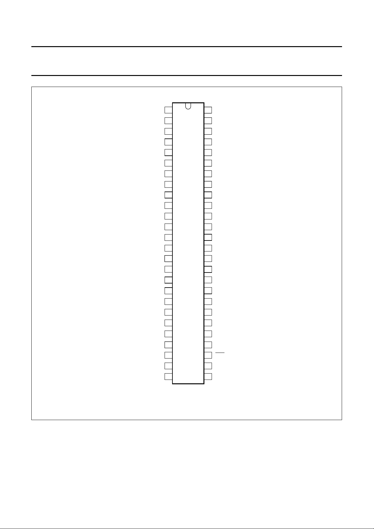
Fig.2 Pin configuration.
35
34
33
32
31
30
29
28
27
VDS
R
G
B
RGBREF
P3.4
COR
V
SSD2
FRAME
February 1995 6
Page 7
Philips Semiconductors Preliminary specification
One page Economy Teletext/TV
microcontroller
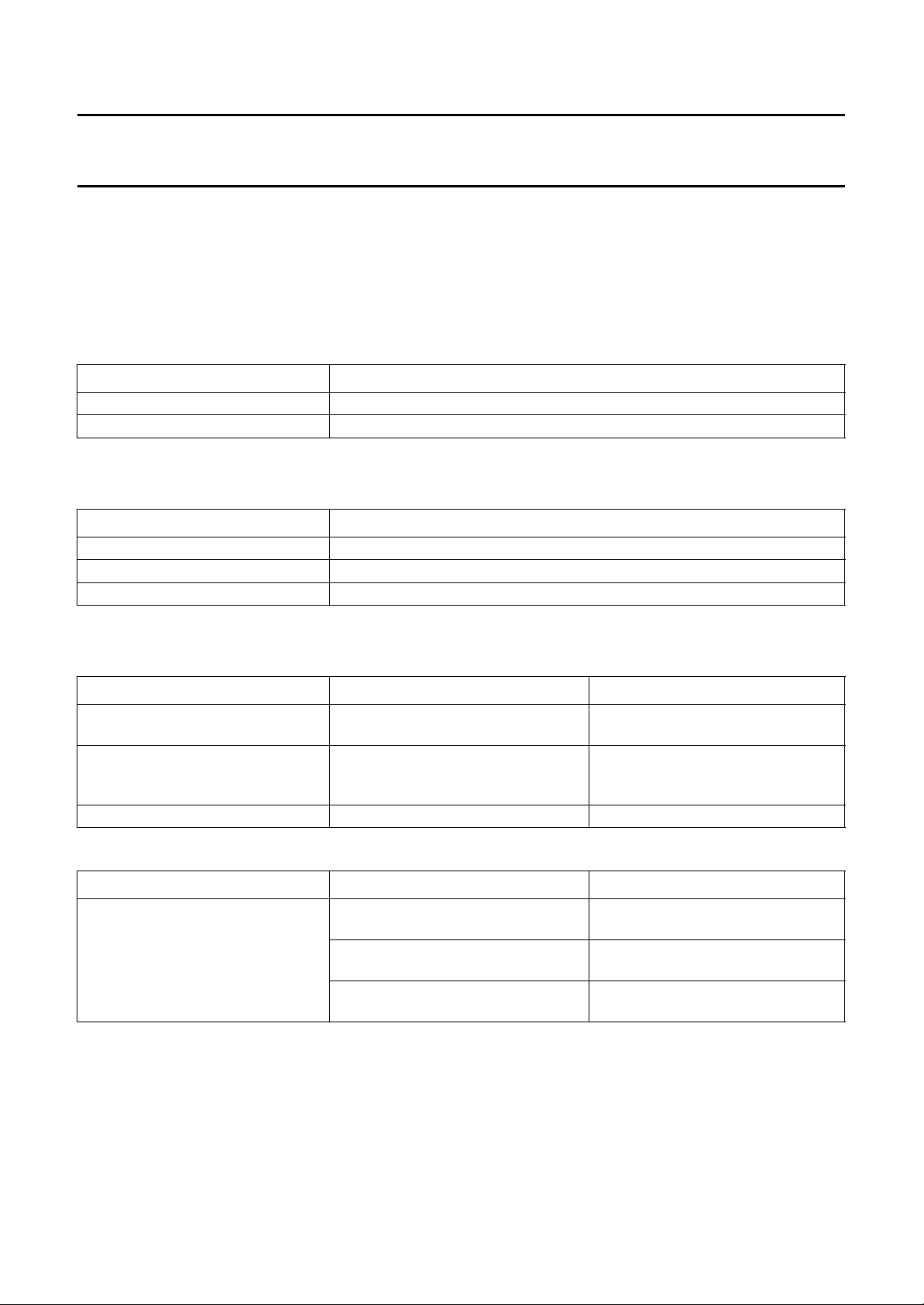
QUALITY AND RELIABILITY
This device will meet Philips Semiconductors General Quality Specification for Business group
Circuits SNW-FQ-611-Part E”
requirements are shown in Tables 1 to 4.
Group A
Table 1 Acceptance tests per lot
TEST REQUIREMENTS
Mechanical cumulative target: <80 ppm
Electrical cumulative target: <80 ppm
Group B
Table 2 Processability tests (by package family)
TEST REQUIREMENTS
Solderability <7% LTPD
Mechanical <15% LTPD
Solder heat resistance <15% LTPD
(see
“Quality Reference Handbook”
, order number 9398 510 63011). The principal
(1)
(1)
SAA5290
“Consumer Integrated
Group C
Table 3 Reliability tests (by process family)
TEST CONDITIONS REQUIREMENTS
Operational life 168 hours at Tj= 150 °C <1500 FPM; equivalent to
<100 FITS at Tj =70°C
Humidity life temperature, humidity, bias
<2000 FPM
1000 hours, 85 °C, 85% RH
(or equivalent test)
Temperature cycling performance T
stg(min)
to T
stg(max)
<2000 FPM
Table 4 Reliability tests (by device type)
TEST CONDITIONS REQUIREMENTS
ESD and latch-up ESD Human body model
<15% LTPD
2000 V, 100 pF, 1.5 kΩ
ESD Machine model
<15% LTPD
200 V, 200 pF, 0 Ω
latch-up 100 mA, 1.5 × V
DD
<15% LTPD
(absolute maximum)
Notes to Tables 1 to 4
1. ppm = fraction of defective devices, in parts per million.
LTPD = Lot Tolerance Percent Defective.
FPM = fraction of devices failing at test condition, in Failures Per Million.
FITS = Failures In Time Standard.
(1)
(1)
February 1995 7
Page 8

Philips Semiconductors Preliminary specification
One page Economy Teletext/TV
SAA5290
microcontroller
LIMITING VALUES
In accordance with Absolute Maximum Rating System (IEC 134).
SYMBOL PARAMETER CONDITIONS MIN. MAX. UNIT
V
DD
V
I
V
O
I
O
I
IOK
∆V
SS
∆V
DD
T
amb
T
stg
Notes
1. This maximum value has an absolute maximum of 6.5 V independent of V
2. Except in standby mode.
supply voltage (all supplies) −0.3 +6.5 V
input voltage (any input) note 1 −0.3 VDD+ 0.5 V
output voltage (any output) note 1 −0.3 VDD+ 0.5 V
output current (each output) −±10 mA
DC input or output diode current −±20 mA
difference between V
difference between V
SSD
DDM
, V
and OSCGND −±0.1 V
SSA
, V
DDT
and V
DDA
note 2 −±0.1 V
operating ambient temperature −20 +70 °C
storage temperature −55 +125 °C
.
DD
CHARACTERISTICS
VDD=5V±10%; VSS=0V; T
= −20 to +70 °C; unless otherwise specified.
amb
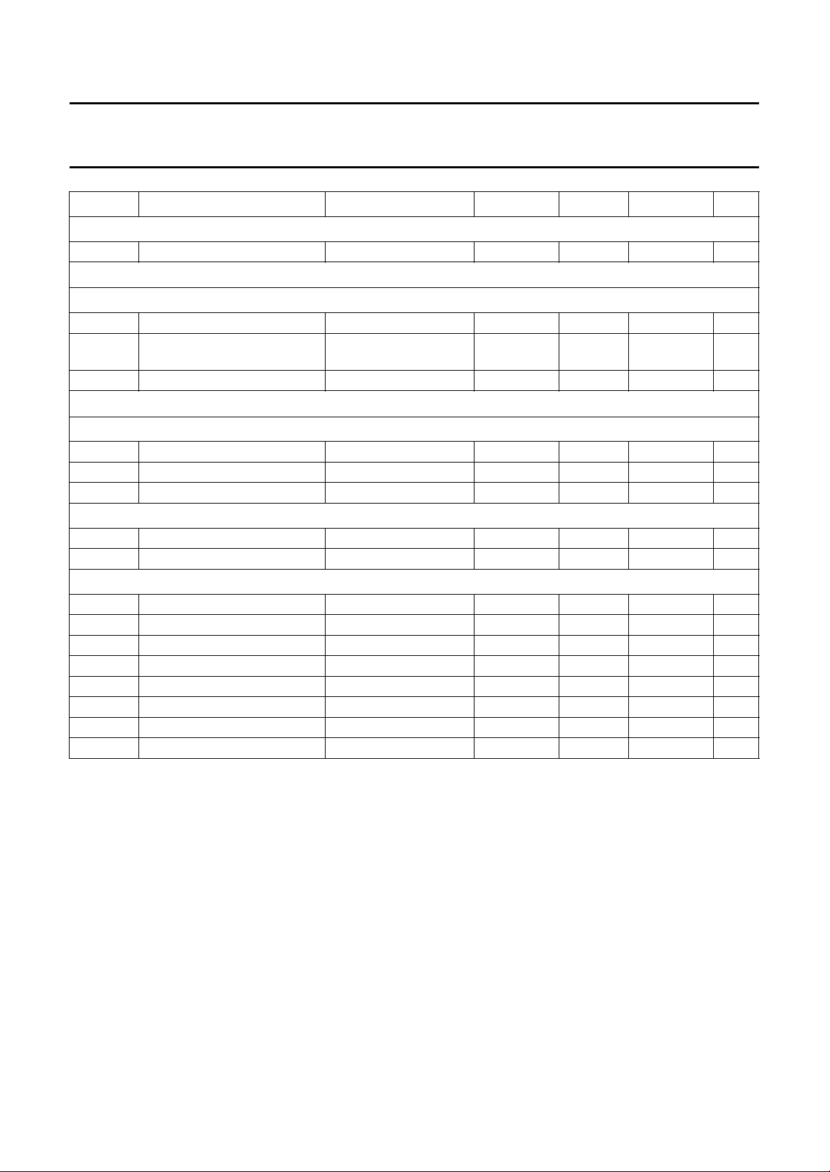
SYMBOL PARAMETER CONDITIONS MIN. TYP. MAX. UNIT
Supplies
V
DD
I
DDM
I
DDA
I
DDT
supply voltage (VDD to VSS) 4.5 5.0 5.5 V
microcontroller supply current − 25 40 mA
analog supply current − 35 50 mA
teletext supply current − 20 30 mA
Digital inputs
RESET
V
IL
V
IH
I
LI
C
I
LOW level input voltage −0.3 − 0.2VDD− 0.1 V
HIGH level input voltage 0.7V
input leakage current VI= 0 to V
DD
−10 − +10 µA
DD
− VDD+ 0.3 V
input capacitance −−4pF
HSYNC AND VSYNC
V
thf
V
thr
V
HYS
C
I
switching threshold falling 0.2V
DD
switching threshold rising −−0.8V
hysteresis voltage − 0.33V
input capacitance −−4pF
−− V
V
− V
DD
DD
February 1995 8
Page 9
Philips Semiconductors Preliminary specification
One page Economy Teletext/TV
SAA5290
microcontroller
SYMBOL PARAMETER CONDITIONS MIN. TYP. MAX. UNIT
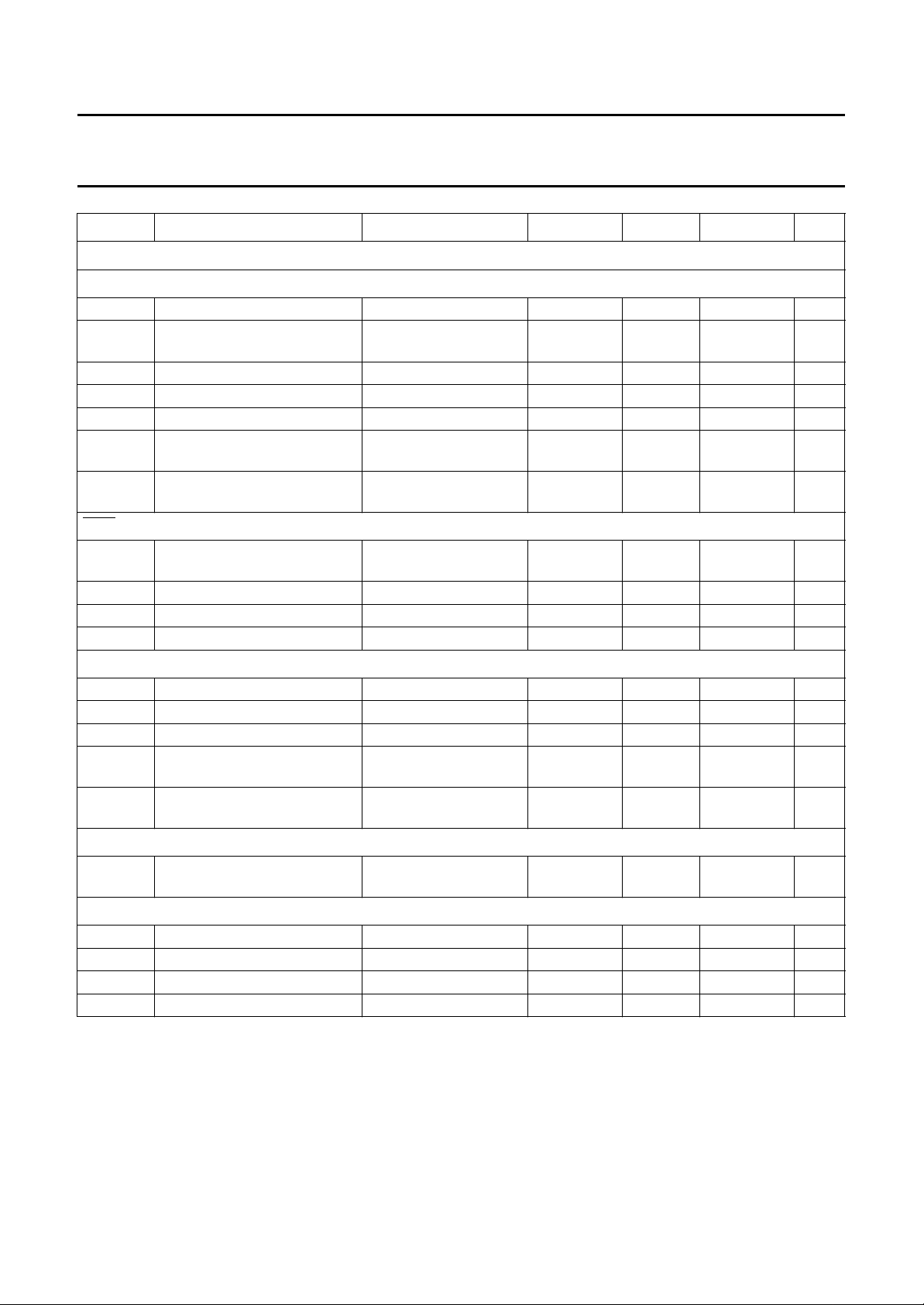
Digital outputs
R, G AND B (note 1)
V
OL
V
OH
| output impedance −−150 Ω
|Z
O
C
L
I
O
t
r
t
f
COR (OPEN-DRAIN OUTPUT)
V
OH
V
OL
I
OL
C
L
VDS
V
OL
V
OH
C
L
t
r
t
f
R, G, B AND VDS
t
skew
FRAME
V
OH
V
OL
I
OL
C
L
LOW level output voltage IOL= 2 mA 0 − 0.2 V
HIGH level output voltage IOH= −2mA V
RGBREF
− 0.3
V
RGBREFVRGBREF
+ 0.4
V
load capacitance −−50 pF
DC output current −−−4mA
output rise time between 10% and 90%;
−−20 ns
CL=50pF
output fall time between 90% and 10%;
−−20 ns
CL=50pF
HIGH level pull-up output
−−VDDV
voltage
LOW level output voltage IOL= 2 mA 0 − 0.5 V
LOW level output current −−2mA
load capacitance −−25 pF
LOW level output voltage IOL= 1.6 mA 0 − 0.2 V
HIGH level output voltage IOH= −1.6 mA VDD− 0.3 − VDD+ 0.4 V
load capacitance −−50 pF
output rise time between 10% and 90%;
−−20 ns
CL=50pF
output fall time between 90% and 10%;
−−20 ns
CL=50pF
skew delay between any two
−−20 ns
pins
HIGH level output voltage IOL= 8 mA 0 − 0.5 V
LOW level output voltage IOL= −8mA VDD− 0.5 − V
DD
V
LOW level output current −8 − +8 mA
load capacitance −−100 pF
February 1995 9
Page 10

Philips Semiconductors Preliminary specification
One page Economy Teletext/TV
SAA5290
microcontroller
SYMBOL PARAMETER CONDITIONS MIN. TYP. MAX. UNIT
Digital input/outputs
P0.0 TO P0.4, P0.7, P1.0 TO P1.5, P2.0 TO P2.7 AND P3.0 TO P3.5
V
IL
V
IH
C
I
V
OL
C
L
P0.5 AND P0.6
V
IL
V
IH
C
I
V
OL
C
L
P1.6 AND P1.7
V
IL
V
IH
C
I
V
OL
C
L
t
f
Analog inputs
LOW level input voltage −0.3 − 0.2VDD− 0.1 V
HIGH level input voltage 0.2VDD+ 0.9 − VDD+ 0.3 V
input capacitance −−4pF
LOW level output voltage IOL= 3.2 mA 0 − 0.45 V
load capacitance −−50 pF
LOW level input voltage −0.3 − 0.2VDD− 0.1 V
HIGH level input voltage 0.2VDD+ 0.9 − VDD+ 0.3 V
input capacitance −−4pF
LOW level output voltage IOL=10mA 0 − 0.45 V
load capacitance −−50 pF
LOW level input voltage −0.3 − +1.5 V
HIGH level input voltage 3.0 − VDD+ 0.3 V
input capacitance −−5pF
LOW level output voltage IOL= 3 mA 0 − 0.5 V
load capacitance −−400 pF
output fall time between 3 and 1 V −−200 ns
CVBS0
V
V
sync
vid(p-p)
AND CVBS1
sync voltage amplitude 0.1 0.3 0.6 V
video input voltage amplitude
0.7 1.0 1.4 V
(peak-to-peak value)
Z
source
V
IH
| input impedance 2.5 5.0 − kΩ
|Z
I
C
I
source impedance −−250 Ω
HIGH level input voltage 3.0 − VDD+ 0.3 V
input capacitance −−10 pF
IREF
R
gnd
resistor to ground − 27 − kΩ
RGBREF (note 1)
V
I
I
I
input voltage −0.3 − V
DD
DC input current −−12 mA
February 1995 10
V
Page 11
Philips Semiconductors Preliminary specification
One page Economy Teletext/TV
SAA5290
microcontroller
SYMBOL PARAMETER CONDITIONS MIN. TYP. MAX. UNIT
ADC0, ADC1
V
IL
Analog input/output
BLACK
C
black
V
black
I
LI
Crystal oscillator
OSCIN
V
IL
V
IH
C
I
OSCOUT
f
osc
C
O
CRYSTAL SPECIFICATION (note 2)
f
xtal
C
L
C1 series capacitance T
C0 parallel capacitance T
R
r
T
xtal
X
j
X
d
Notes
1. All RGB current is sourced from the RGBREF pin. The maximum effective series resistance between RGBREF and
the R, G and B pins is 150 Ω.
2. Crystal order number 4322 143 05561.
AND ADC2
LOW level input voltage −0.3 − V
DD
V
storage capacitor to ground − 100 − nF
black level voltage for nominal
1.8 2.15 2.5 V
sync amplitude
input leakage current −10 − +10 µA
LOW level input voltage −0.3 − 0.2VDD− 0.1 V
HIGH level input voltage 0.7V
DD
− VDD+ 0.3 V
input capacitance −−10 pF
crystal oscillator frequency − 12 − MHz
output capacitance −−10 pF
nominal frequency − 12 − MHz
load capacitance − 32 − pF
=25°C − 18.5 − fF
amb
=25°C − 4.9 − pF
amb
resonance resistance T
=25°C − 35 −Ω
amb
temperature range −20 +25 +70 °C
adjustment tolerance T
=25°C −−±50 × 10
amb
drift −−±30 × 10
−6
−6
February 1995 11
Page 12
Philips Semiconductors Preliminary specification
One page Economy Teletext/TV
microcontroller
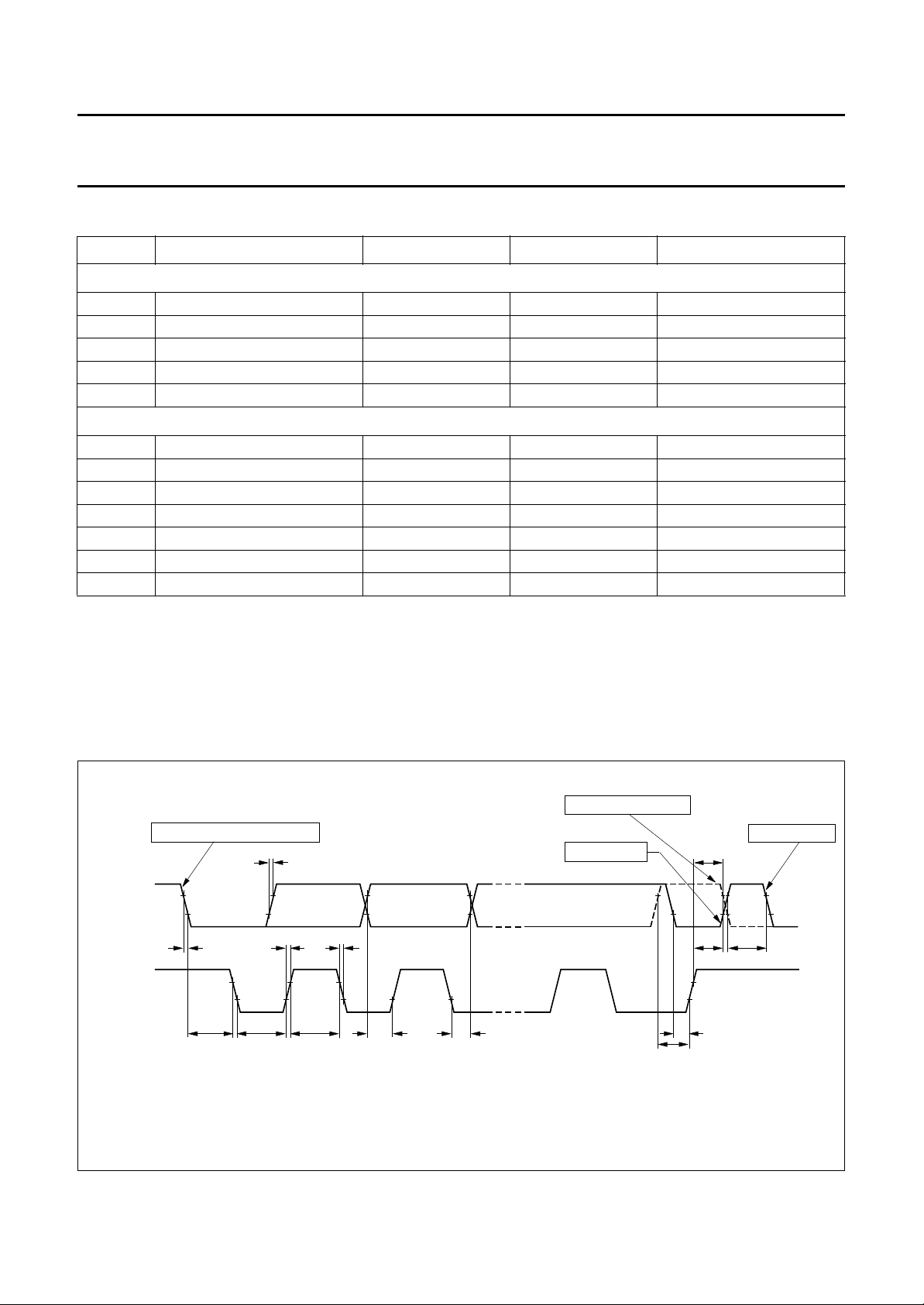
Table 5 Characteristics for the I2C-bus interface
SYMBOL PARAMETER INPUT OUTPUT I
SCL timing
t
HD;STA
t
LOW
t
HIGH
t
rC
t
fC
SDA timing
t
SU;DAT1
t
HD;DAT
t
SU;STA
t
SU;STO
t
BUF
t
rD
t
fD
START condition hold time ≥4.0 µs note 1 ≥4.0 µs
SCL LOW time ≥4.7 µs note 1 ≥4.7 µs
SCL HIGH time ≥4.0 µs ≥4.0 µs; note 2 ≥4.0 µs
SCL rise time ≤1.0 µs note 3 ≤1.0 µs
SCL fall time ≤0.3 µs ≤0.3 µs; note 4 ≤0.3 µs
data set-up time ≥250 ns note 1 ≥250 ns
data hold time ≥0 ns note 1 ≥0ns
repeated START set-up time ≥4.7 µs note 1 ≥4.7 µs
STOP condition set-up time ≥4.0 µs note 1 ≥4.0 µs
bus free time ≥4.7 µs note 1 ≥4.7 µs
SDA rise time ≤1.0 µs note 3 ≤1.0 µs
SDA fall time ≤0.3 µs ≤0.3 µs; note 4 ≤0.3 µs
SAA5290
2
C-BUS SPECIFICATION
Notes
2
1. This parameter is determined by the user software. It must comply with the I
C-bus specification.
2. This value gives the auto-clock pulse length which meets the I2C-bus specification for the special crystal frequency.
Alternatively, the SCL pulse must be timed by software.
3. The rise time is determined by the external bus line capacitance and pull-up resistor. It must be less than 1 µs.
4. The maximum capacitance on bus lines SDA and SCL is 400 pF.
repeated START condition
SDA
(input / output)
SCL
(input / output)
START or repeated START condition
t
rD
t
t
HD;STA
fD
t
rC
t
LOWtHIGH
t
t
SU;DAT2
SU;STA
t
SU;STO
0.7V
0.3V
t
SU;DAT3
STOP condition
t
fC
t
SU;DAT1
t
HD;DAT
t
DD
DD
START condition
0.7V
0.3V
BUF
MLC104
DD
DD
Fig.3 I2C-bus interface timing.
th
February 1995 12
Page 13

Philips Semiconductors Preliminary specification
One page Economy Teletext/TV
microcontroller
FUNCTIONAL DESCRIPTION
Introduction
The SAA5290 is an integrated teletext decoder and
microcontroller. The teletext decoder is derived from the
SAA5254 single page teletext decoder IC, with a number
of enhancements to increase its suitability for on-screen
display applications. The microcontroller is a derivative of
the industry standard 80C51 microcontroller. A block
diagram of the SAA5290 is given in Fig.1.
Microcontroller
The functionality of the microcontroller used on the
SAA5290 is described here with reference to the industry
standard 80C51 microcontroller. A full description of its
functionality can be found in the handbook
8-bit microcontrollers IC20
reference, the changes made for the SAA5290 fall into two
categories, features not supported by the SAA5290 and
features found on the SAA5290 but not supported by the
80C51.
. Using the 80C51 as a
80C51-based
SAA5290
OFF-CHIP MEMORY
The SAA5290 does not support the use of off-chip
program memory or off-chip data memory. This means
that the SAA5290 does not have any of EA,RD, WR, ALE
or PSEN pins. The 4 MOVX instructions which move data
to and from external RAM should not be used.
I
DLE AND POWER-DOWN MODES
Idle and power-down modes are not supported by the
SAA5290. As a consequence, the respective bits in PCON
are not available.
FUNCTION
UART
The 80C51 UART is not available in the SAA5290. As a
consequence the SCON and SBUF SFRs are removed
and the ES bit in the IE SFR is unavailable.
Additional features for the SAA5290
The following features are provided by the SAA5290 in
addition to the standard 80C51 features.
80C51 features not supported by the SAA5290
NTERRUPT PRIORITY
I
The IP SFR is not implemented and all interrupts are
treated with the same priority level. The SAA5290 retains
the normal prioritization of interrupts within a level.
Table 6 Interrupts and their vector addresses
EVENT PROGRAM MEMORY ADDRESS
Reset 000H
External INT0 003H
Timer 0 00BH
External INT1 013H
Timer 1 01BH
2
I
C-bus 053H
INTERRUPTS
The external INT1 interrupt is modified to generate an
interrupt on both the rising and falling edges of the INT1
pin, when EX1 bit is set. This facility allows for software
pulse width measurement for handling of a remote control.
IT LEVEL I
B
The bit-level serial I/O supports the I2C-bus. P1.6/SCL and
P1.7/SDA are the serial I/O pins. These two pins meet the
I2C-bus specification concerning the input levels and
output drive capability. Consequently, these pins have an
open-drain output configuration. All the four following
modes of the I2C-bus are supported.
• Master transmitter
• Master receiver
• Slave transmitter
2
C-BUS INTERFACE
February 1995 13
Page 14

Philips Semiconductors Preliminary specification
One page Economy Teletext/TV
microcontroller
• Slave receiver.
The advantages of the bit-level I2C-bus hardware,
compared with a full software I2C-bus implementation are:
• The hardware can generate the SCL pulse
• Testing a single bit (RBF or WBF respectively) is
sufficient as a check for error-free transmission.
The bit-level I2C-bus hardware operates on serial bit level
and performs the following functions:
• Filtering the incoming serial data and clock signals
• Recognizing the START condition
• Generating a serial interrupt request SI after reception of
a START condition and the first falling edge of the serial
clock
• Recognizing the STOP condition
• Recognizing a serial clock pulse on the SCL line
• Latching a serial bit on the SDA line (SDI)
• Stretching the SCL LOW period of the serial clock to
suspend the transfer of the next serial data bit
• Setting Read Bit Finished (RBF) when the SCL clock
pulse has finished and Write Bit Finished (WBF) if there
is no arbitration loss detected (i.e. SDA = logic 0 while
SDO = logic 1)
• Setting a serial clock LOW-to-HIGH detected (CLH) flag
• Setting a Bus Busy (BB) flag on a START condition and
clearing this flag on a STOP condition
• Releasing the SCL line and clearing the CLH, RBF and
WBF flags to resume transfer to the next serial data bit
• Generating an automatic clock if the single bit data
register S1BIT is used in master mode.
The following functions must be done in software:
• Handling the I2C-bus START interrupts
• Converting serial data to parallel data when receiving
• Converting parallel data to serial data when transmitting
• Comparing the received slave address with its own
address
• Interpreting the acknowledge information
• Guarding the I2C-bus status if RBF or WBF = logic 0.
Additionally, if acting as master:
• Generating START and STOP conditions
• Handling bus arbitration
• Generating serial clock pulses if S1BIT is not used.
SAA5290
LED
SUPPORT
Port pins P0.5 and P0.6 have a 10 mA current sinking
capability to enable LEDs to be driven directly.
PWM DAC
The SAA5290 has six 6-bit PWM DACs and one14-bit
PWM DAC. These allow direct control of other parts of the
television.
The low resolution 6 bit DACs are controlled by their
corresponding SFR (PWM0 to PWM5) and are connected
as alternative outputs of Port P2. The port bit
corresponding to the PWM should be set to logic 1 for
correct operation of the PWM.
Table 7 Special Function Registers PWM0 to PWM5
D7 D6 D5 D4 D3 D2 D1 D0
PWE − PV5 PV4 PV3 PV2 PV1 PV0
If the PWE bit for a particular port is set to logic 1, the PWM
is active and controls its assigned port pin. If the PWE bit
is set to logic 0 the corresponding port pin is controlled by
the bit in the corresponding port register for that port.
The output of the PWM is a pulse of period 21.33 µs with
a duty cycle determined by the binary value, PV5 to PV0,
multiplied by 0.33 µs. The 14 bit PWM is controlled with
SFR registers TDACL and TDACH.
Table 8 Special Function Register TDACL
D7 D6 D5 D4 D3 D2 D1 D0
TD7 TD6 TD5 TD4 TD3 TD2 TD1 TD0
Table 9 Special Function Register TDACH
D7 D6 D5 D4 D3 D2 D1 D0
PWE − TD13 TD12 TD11 TD10 TD9 TD8
If the PWE bit is set to logic 1, the TPWM is active and
controls Port P2.0. If the PWE bit is set to logic 0 the port
pin is controlled by the bit in the corresponding port
register for P2.0.
The output of the TPWM is a pulse of period 42.66 µs with
a duty cycle determined by the binary value, TD13 to TD7,
multiplied by 0.33 µs.
S
Three SFRs support the function of the bit-level I2C-bus
hardware, they are S1INT, S1BIT and S1SCS.
February 1995 14
Page 15

Philips Semiconductors Preliminary specification
One page Economy Teletext/TV
microcontroller
The 7 least significant bits, TD6 to TD0, extend the HIGH
time of a proportion of the pulses by 0.33 µs. If the LSB is
set then 1 in 128 cycles is extended, if bit 1 is set then
1 in 64 cycles is extended, and so on.
OFTWARE ADC
S
Up to 3 successive approximation ADCs can be
implemented in software by making use of the on-board
4-bit DAC and multiplexed voltage comparator. The
software ADC uses 3 analog inputs which are multiplexed
with P3.0 to P3.2.
The control of the ADC is achieved using the SAD SFR.
SAD.5 and SAD.6 select one of the three inputs to pass to
the comparator. The other input comes from the DAC
whose input is set by SAD bits 0 to 3. The output of the
comparator is SAD bit 7 and is valid by the next instruction
after starting the comparison by setting SAD.ST to logic 1.
Microcontroller interfacing
SAA5290
The 80C51 CPU communicates with the peripheral
functions using Special Function Registers (SFRs) which
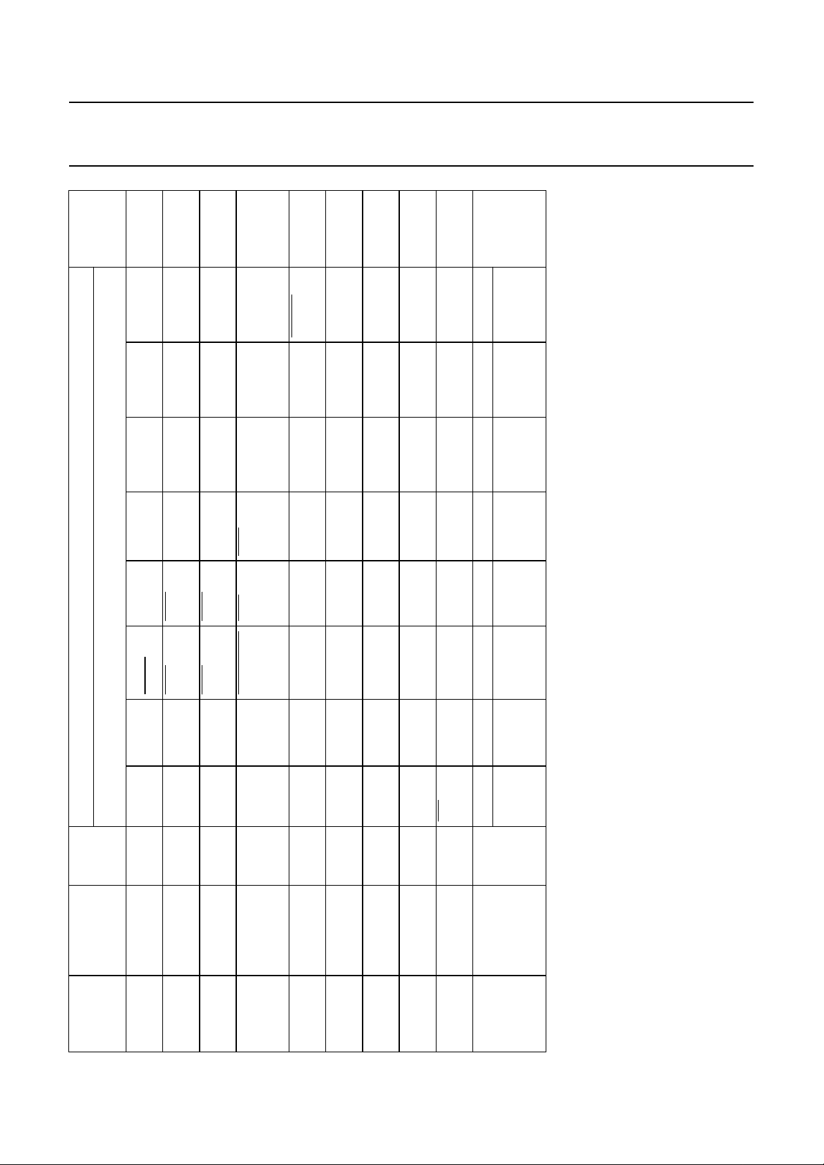
are addressed as RAM locations. The registers in the
teletext decoder appear as normal SFRs in the
microcontroller memory map, but are written to using a
serial bus. This bus is controlled by dedicated hardware
which uses a simple handshake system for software
synchronization. The SFR memory map is given in
Table 10.
February 1995 15
Page 16

Philips Semiconductors Preliminary specification
One page Economy Teletext/TV
microcontroller
(HEX)
VALUE
SAA5290
BIT ADDRESS, SYMBOL OR ALTERNATIVE PORT FUNCTION RESET
Table 10 SAA5290 Special Function Register map (note 1)
MSB LSB
(HEX)
ADDR.
DIRECT
SYMBOL DESCR.
Accumulator E0H E7 E6 E5 E4 E3 E2 E1 E0 00H
(2)
ACC
B register F0H F7 F6 F5 F4 F3 F2 F1 F0 00H
(2)
B
DPTR: Data Pointer
(2 bytes):
DPH High byte 83H −−−−−−−−00H
DPL Low byte 82H −−−−−−−−00H
EA ES1 ∗∗ET1 EX1 ET0 EX0
A8H AF AE AD AC AB AA A9 A8 X0H
Interrupt
Enable
(2)(3)
IE
Port 0 80H 87 86 85 84 83 82 81 80 FFH
(2)
P0
Port 1 90H 97 96 95 94 93 92 91 90 FFH
(2)
P1
Port 2 A0H A7 A6 A5 A4 A3 A2 A1 A0 FFH
(2)
P2
Port 3 B0H −− − B4 B3 B2 B1 B0 XXX11111B
(2)(3)
P3
87H ∗∗ ∗ ∗ GF1 GF0 ∗∗XXXX00XXB
Power
(3)
PCON
February 1995 16
D0H D7 D6 D5 D4 D3 D2 D1 D0 000000X0B
Control
Program
(2)
PSW
CY AC F0 RS1 RS0 0V ∗ P
D5H PWE ∗ PV5 PV4 PV3 PV2 PV1 PV0 −
Status Word
Pulse Width
(3)
PWM0
D6H PWE ∗ PV5 PV4 PV3 PV2 PV1 PV0 −
Modulator 0
Pulse Width
Modulator 1
(3)
PWM1
D7H PWE ∗ PV5 PV4 PV3 PV2 PV1 PV0 −
DCH PWE ∗ PV5 PV4 PV3 PV2 PV1 PV0 −
Pulse Width
Modulator 2
Pulse Width
(3)
(3)
PWM2
PWM3
DDH PWE ∗ PV5 PV4 PV3 PV2 PV1 PV0 −
Modulator 3
Pulse Width
Modulator 4
(3)
PWM4
∗∗∗∗∗∗∗00H
DEH PWE ∗ PV5 PV4 PV3 PV2 PV1 PV0 −
D9H SDI/
C
2
Pulse Width
Modulator 5
Serial I
(3)
(3)
PWM5
S1BIT
SDO
data
Page 17

Philips Semiconductors Preliminary specification
One page Economy Teletext/TV
microcontroller
(HEX)
VALUE
∗∗00H
DISABLE
FRAME
SAA5290
00H
V
POLARITY
H
POLARITY
FIELD
POLARITY
BIT ADDRESS, SYMBOL OR ALTERNATIVE PORT FUNCTION RESET
MSB LSB
(HEX)
ADDR.
DIRECT
CLH BB RBF WBF STR ENS
SCI/
SDO
SDO
E8H EF EE ED EC EB EA E9 E8 00H
VHI CH1 CH0 ST SAD3 SAD2 SAD1 SAD0
88H TF1 TR1 TF0 TR0 IE1 IT1 IE0 IT0 00H
D3H PWE ∗ TD13 TD12 TD11 TD10 TD9 TD8 00H
D2H TD7 TD6 TD5 TD4 TD3 TD2 TD1 TD0 00H
8CH −−−−−−−−00H
SDI/
DAH SI ∗∗∗∗∗∗∗−
D8H DF DE DD DC DB DA D9 D8 −
C
C
2
2
8DH −−−−−−−−00H
8AH −−−−−−−−00H
8BH −−−−−−−−00H
TM1 M0GATEC/T M1 M0 00H
89H GATE C/
DISPLAY
STATUS
ROW
DISABLE
HDR
ROLL
FRAME
∗ AUTO
POS
C0H X24
ONLY
FIELD
C1H ∗ 8-BIT ACQ OFF X26 FULL
C2H ∗∗ ∗ ∗ ∗ SC2 SC1 SC0 00H
C3H ∗∗ ∗ PRD4 PRD3 PRD2 PRD1 PRD0 00H
Serial I
(3)
SYMBOL DESCR.
interrupt
S1INT
Serial I
(2)(3)
S1SCS
control
Software
AtoD
(2) (3)
SAD
Timer/counter
control
(2)
SP Stack Pointer 81H 8F 8E 8D 8C 8B 8A 89 88 07H
TCON
High byte
TDACH TPWM
Low byte
TDACL TPWM
TH0 Timer 0
February 1995 17
High byte
High byte
TH1 Timer 1
Low byte
TL0 Timer 0
Low byte
TL1 Timer 1
mode
Teletext
register 0
(3)
TXT0
TMOD Timer/counter
Teletext
register 1
(3)
TXT1
Teletext
register 2
(3)
TXT2
Teletext
register 3
(3)
TXT3
Page 18
Philips Semiconductors Preliminary specification
One page Economy Teletext/TV
microcontroller
(HEX)
VALUE
00000011B
00H
PICTURE
SHADOW
ENABLE
TRANS
ENABLE
TEXT IN PICTURE
C MESH
ENABLE
00000011B
ON IN
PICTURE
ON IN
ON OUT
ON OUT
TEXT IN PICTURE
BOX ON 0 00H
BOX ON
1-23
BOX ON
24
00H
CVBS1
QUALITY
TXT ON VIDEO
ROM
VER R0
I/FACE
SAA5290
BUSY
BIT ADDRESS, SYMBOL OR ALTERNATIVE PORT FUNCTION RESET
MSB LSB
(HEX)
ADDR.
DIRECT
ENABLE
∗ B MESH
WEST
COR OUT COR IN TEXT
BKGND
C4H ∗∗ EAST/
C5H BKGND
OUT
IN
OUT
OUT
COR OUT COR IN TEXT
BKGND
IN
OUT
C6H BKGND
SNG/DBL
HEIGHT
TOP/
BTM
CONCEAL
/REVEAL
CURSOR
ON
ROW
TOP
C7H STATUS
C8H ∗∗ ∗ ∗ ∗ ∗ ∗ CVBS0/
A0 R4 R3 R2 R1 R0 00H
MEM.
C9H ∗ CLEAR
CAH ∗∗ C5 C4 C3 C2 C1 C0 00H
CBH D7 D6 D5 D4 D3 D2 D1 D0 00H
ROM
VER R1
ROM
VER R2
ROM
VER R3
ROM
VER R4
SYNC
CCH 625/525
∗∗ ∗ ∗ ∗ ∗ ∗ TXT
B8H BF BE BD BC BB BA B9 B8 00H
Teletext
register 4
Teletext
register 5
Teletext
register 6
Teletext
register 7
Teletext
register 8
Teletext
register 9
Teletext
register 10
(3)
SYMBOL DESCR.
TXT4
(3)
TXT5
(3)
TXT6
(3)
TXT7
(3)
TXT8
(3)
TXT9
(3)
TXT10
February 1995 18
Teletext
register 11
(3)
TXT11
Teletext
register 12
(3)
TXT12
Teletext
register 13
(2)(3)
TXT13
Notes
1. The star (∗) indicates these bits are inactive and must be written to logic 0 for future compatibility.
2. SFRs are bit addressable.
3. SFRs are modified or added to the 80C51 SFRs.
Page 19
Philips Semiconductors Preliminary specification
One page Economy Teletext/TV
microcontroller
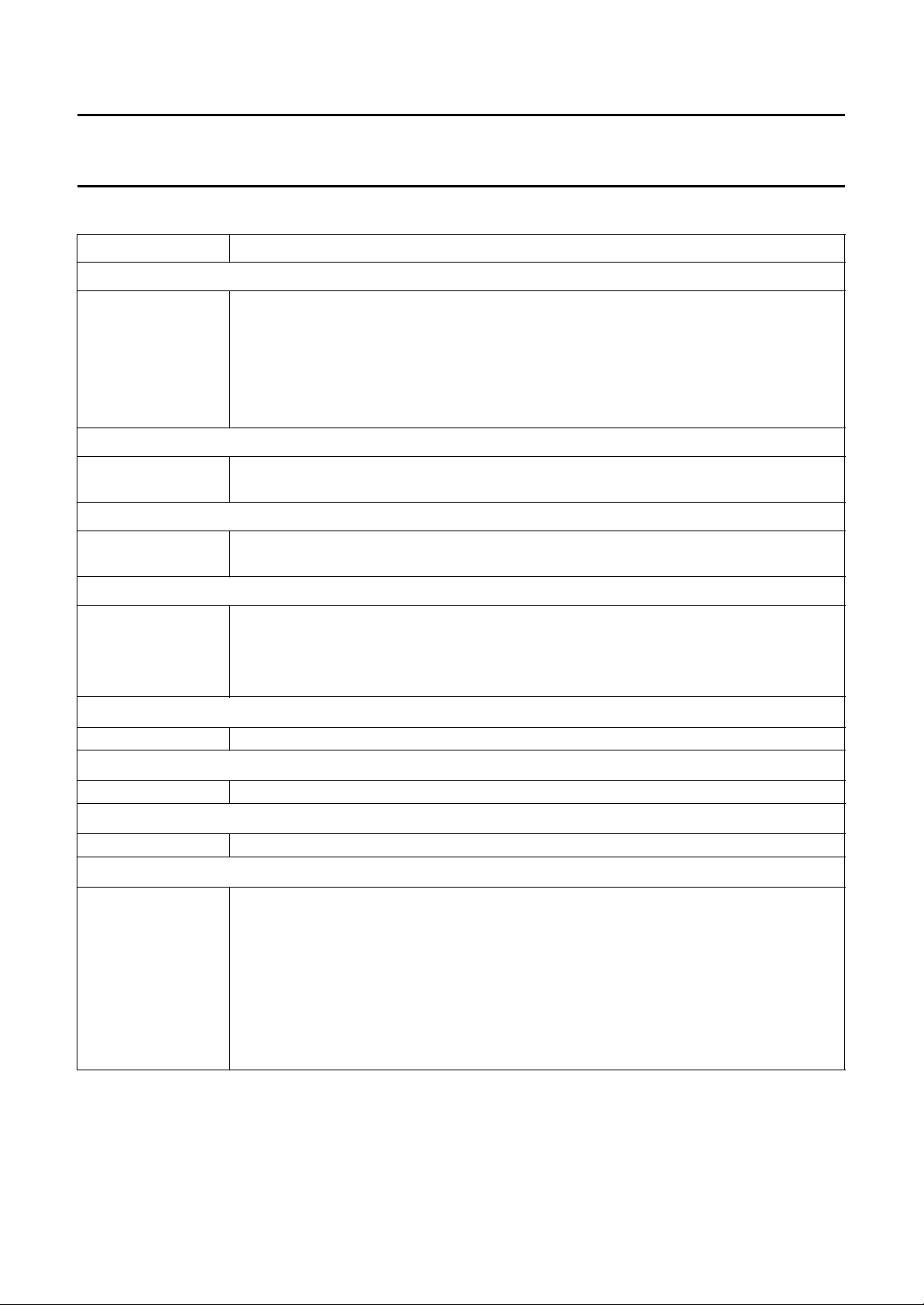
Table 11 SFR description
REGISTER FUNCTION
IE - Interrupt Enable
EA Disable all interrupts (logic 0) or use individual enable bits (logic 1).
2
ES1 I
ET1 Enable Timer 1 overflow interrupt (logic 1).
EX1 Enable external interrupt 1 (logic 1).
ET0 Enable Timer 0 overflow interrupt (logic 1).
EX0 Enable external interrupt 0 (logic 1).
PCON - Power Control
GF0 General purpose flag bit 0.
GF1 General purpose flag bit 1.
PWM0 to PWM5 - 6-bit Pulse Width Modulator control registers
PWE Activate this 6-bit PWM and take over port pin (logic 1).
PV0 to PV5 Value to output by this 6-bit PWM.
C-bus interrupt enable (logic 1).
SAA5290
SAD - Software ADC control
VHI Analog input voltage greater than DAC output voltage (logic 1).
CH0 and CH1 See Table 12.
ST Initiate voltage comparison (logic 1). This is automatically reset.
SAD0 to SAD3 4-bit DAC input value. The DAC output of this value is compared with analog input voltage.
2
S1BIT - Serial I
SDI I
S1BIT - Serial I
SDO I
S1INT - Serial I
SI I
S1SCS - Serial I
C-bus data (READ)
2
C-bus data bit latched-in from SDA on the last rising edge of SCL.
2
C-bus data (WRITE)
2
C-bus data bit output.
2
C-bus interrupt
2
C-bus interrupt flag.
2
C-bus control (READ)
SDI Serial data input at SDA.
SCI Serial clock input at SCL.
CLH Clock LOW-to-HIGH transition flag.
BB Bus busy flag.
RBF Read bit finished flag.
WBF Write bit finished flag.
STR Clock stretching enable (logic 1).
ENS Enable serial I/O (logic 1).
February 1995 19
Page 20
Philips Semiconductors Preliminary specification
One page Economy Teletext/TV
SAA5290
microcontroller
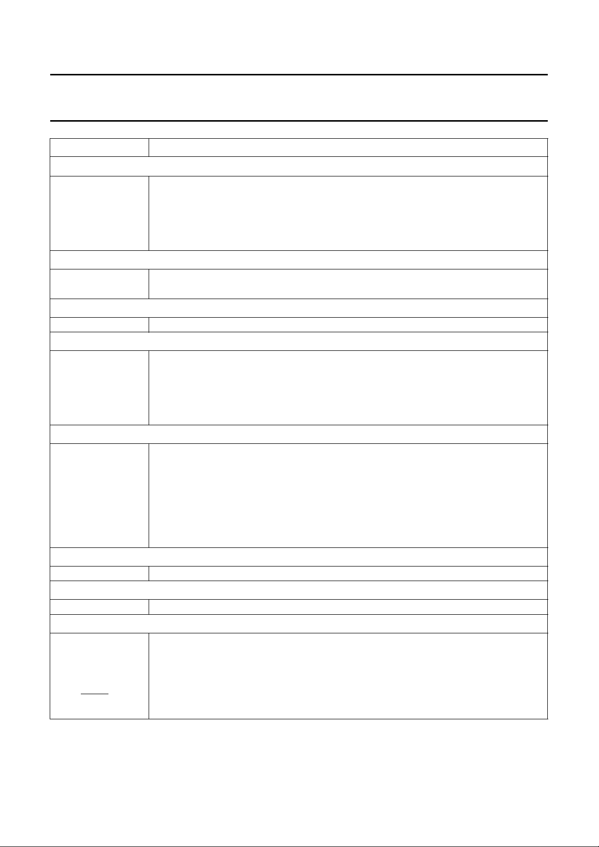
REGISTER FUNCTION
S1SCS - Serial I2C-bus control (WRITE)
SDO Serial data output at SDA.
SCO Serial clock output at SCL.
CLH Clock LOW-to-HIGH transition.
STR Clock stretching enable (logic 1).
ENS Enable serial I/O (logic 1).
TDACH - 14-bit PWM MSB register
PWE Activate this 14-bit PWM and take over port pin (logic 1).
TD8 to TD13 6 LSBs of this value to be output by the 14-bit PWM.
TDACL - 14-bit PWM LSB register
TD0 to TD7 8 LSBs of this value to be output by the 14-bit PWM.
TXT0 - Teletext register 0 (WRITE only)
X24 POSITION Store packet 24 in extension packet memory (logic 0) or page memory (logic 1).
AUTO FRAME Frame output switched off automatically if any video displayed (logic 1).
DISABLE HDR ROLL Do not write rolling headers and time into memory (logic 1).
STATUS ROW ONLY Display only memory row (logic 1).
DISABLE FRAME Frame output always LOW (logic 1).
TXT1 - Teletext register 1 (WRITE only)
8-BIT Data in packets 0 to 24 written into memory without error checking (logic 1).
ACQ OFF Prevent teletext acquisition section writing to memory (logic 1).
X26 Disable automatic processing of packet 26 data (logic 1).
FULL FIELD Accept teletext on TV lines 2 to 22 only (logic 0) or on any line (logic 1).
FIELD POLARITY VSYNC in first half of the line (logic 0) or second half of the line (logic 1) at start of even field.
H POLARITY HSYNC input positive-going (logic 0) or negative-going (logic 1).
V POLARITY VSYNC input positive-going (logic 0) or negative-going (logic 1).
TXT2 - Teletext register 2 (WRITE only)
SC0 to SC2 Start column at which page request data written into TXT3 SFR is placed.
TXT3 - Teletext register 3 (WRITE only)
PRD0 to PRD4 Page request data.
TXT4 - Teletext register 4 (WRITE only)
B MESH ENABLE Enable meshing of area with black background (logic 1).
C MESH ENABLE Enable meshing of area with other background colours (logic 1).
TRANS ENABLE Black background colour is transparent i.e. video is displayed (logic 1).
SHADOW ENABLE Enable south-east shadowing (logic 1).
WEST Western European languages displayed (logic 0) or Eastern European languages displayed
EAST/
(logic 1).
February 1995 20
Page 21
Philips Semiconductors Preliminary specification
One page Economy Teletext/TV
SAA5290
microcontroller
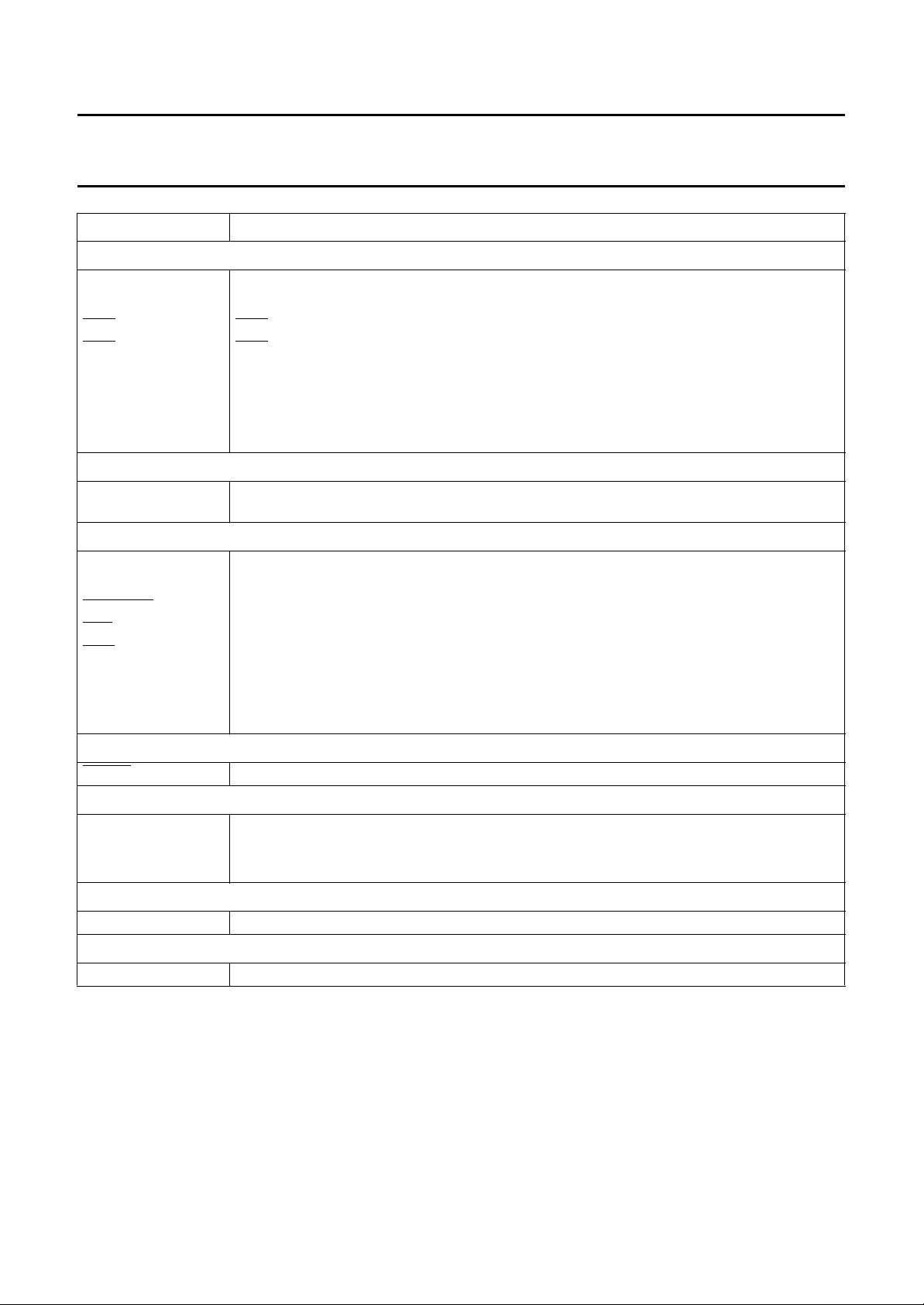
REGISTER FUNCTION
TXT5 - Teletext register 5 (WRITE only)
BKGND OUT Background colour displayed outside teletext boxes (logic 1).
BKGND IN Background colour displayed inside teletext boxes (logic 1).
COR OUT COR output active outside teletext boxes (logic 1).
COR IN COR output active inside teletext boxes (logic 1).
TEXT OUT Text displayed outside teletext boxes (logic 1).
TEXT IN Text displayed inside teletext boxes (logic 1).
PICTURE ON OUT Video picture displayed outside teletext boxes (logic 1).
PICTURE ON IN Video picture displayed inside teletext boxes (logic 1).
TXT6 - Teletext register 6 (WRITE only)
−
TXT7 - Teletext register 7 (WRITE only)
STATUS ROW TOP Display Row 24 below (logic 0) or above (logic 1) teletext page.
CURSOR ON Display cursor at location pointed to by TXT9 and TXT10 (logic 1).
CONCEAL/REVEAL Display characters in areas with the conceal attribute set (logic 1).
TOP/BOTTOM Display Rows 0 to 11 (logic 0) or 12 to 23 (logic 1) when the double height bit is set.
SNG/DBL HEIGHT Display each character at twice normal height (logic 1).
BOX ON 24 Enable teletext boxes in memory Row 24 (logic 1).
BOX ON 1-23 Enable teletext boxes in memory Rows 1 to 23 (logic 1).
BOX ON 0 Enable teletext boxes in memory Row 0 (logic 1).
This register has the same meaning as TXT5 but is only invoked if either newsflash (C5) or the
subtitle (C6) bit in Row 25 of the basic page memory is set.
TXT8 - Teletext register 8 (WRITE only)
CVBS0/CVBS1 CVBS0 input (logic 0) or CVBS1 (logic 1) inputs used for teletext.
TXT9 - Teletext register 9 (WRITE only)
CLEAR MEMORY Write 20H into every location in teletext memory (logic 1).
A0 Access basic page memory (logic 0) or extension packet memory (logic 1) with TXT11 SFR.
R0 to R4 Memory row to be accessed with TXT11 SFR.
TXT10 - Teletext register 10 (WRITE only)
C0 to C5 Memory column to be accessed with TXT11 SFR.
TXT11 - Teletext register 11
D0 to D7 data byte written to, or read from, teletext memory.
February 1995 21
Page 22
Philips Semiconductors Preliminary specification
One page Economy Teletext/TV
SAA5290
microcontroller
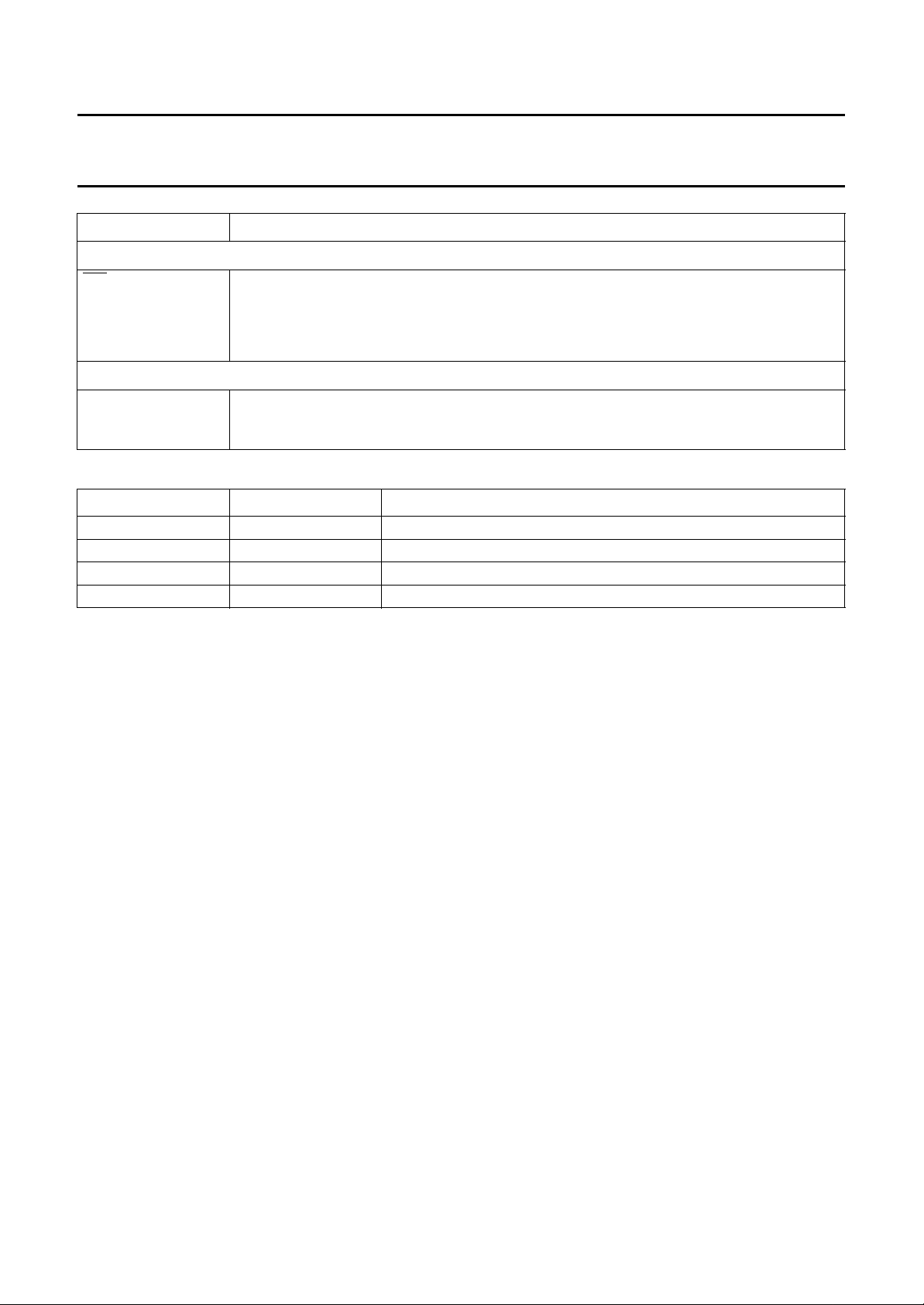
REGISTER FUNCTION
TXT12 - Teletext register 12 (READ only)
625/525 SYNC A 625 line CVBS signal (logic 0), or a 525 line CVBS signal (logic 1) is being input.
ROM VER R0 to R4 Mask programmable to identify character set version.
TXT ON Teletext power has been applied to the device (logic 1).
VIDEO QUALITY CVBS input can be locked on by the teletext decoder (logic 1).
TXT13 - Teletext register 13 (READ only)
TXT I/FACE BUSY Text interface busy and no access for either READ or WRITE is allowed to SFRs
TXT0 to TXT11 (logic 1). This register bit performs the software handshake to the teletext
control registers.
Table 12CH1 and CH0 selection
CH1 CH0 INPUT PIN
0 0 none
0 1 ADC0
1 0 ADC1
1 1 ADC2
February 1995 22
Page 23
Philips Semiconductors Preliminary specification
One page Economy Teletext/TV
microcontroller
TELETEXT DECODER FUNCTIONAL DESCRIPTION
Data slicer
The data slicer extracts the digital teletext data from the
incoming analog waveform. This is performed by sampling
the CVBS waveform and processing the samples to
extract the teletext data and clock.
Acquisition timing
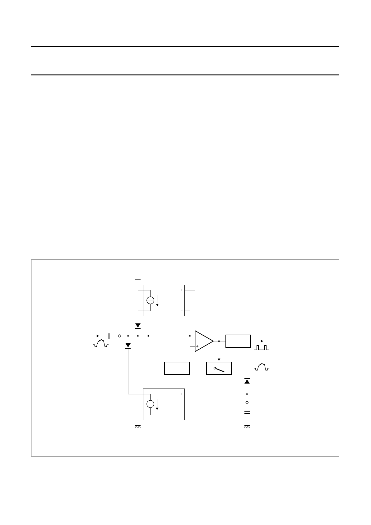
The acquisition timing is generated from a logic level
positive-going composite sync signal ‘VCS’. This signal is
generated by the sync separator circuit which adaptively
slices the sync pulses at 50% of their height. It is able to do
this over a wide range of sync amplitudes by using the
same basic principle used on VIP1 (SAA5230) and VIP2
(SAA5231).
Figure 4 is a block diagram showing the principles of
operation. It relies upon the fact that the ratio of the sync
width to the line time is approximately 13 : 1. In order to
slice the sync pulse at the correct 50% level two currents
are generated.
SAA5290
One is constant and is proportional to the difference
between the black level of the video and the slicing level.
The other is produced only when the video is below the
slicing level, and is also proportional to the difference
between the slicing level and the input, but has a
magnitude13 times greater.
The black level is determined by a sync-gated peak
detector. The video is negatively peak detected into an
external capacitor (BLACK, pin 25), but not during the
sync pulse VCS. The two currents are integrated on the
CVBS input coupling capacitor and the net effect is to alter
the mean input voltage until the (fixed) slicing level is
correct.
The acquisition clocking and timing are locked to the VCS
signal using a digital phased-locked-loop. The phase error
in the acquisition phase-locked-loop is detected by a
signal quality circuit which disables acquisition if poor
signal quality is detected.
handbook, full pagewidth
CVBS
V
DD
V
ref
1/3V (mA)
i
V
(= slicing level)
1/39V (mA)
ref
FILTER
gated negative peak detector
i
V
ref
Fig.4 Sync separator block diagram.
FILTER
VCS
BLACK
MLC105
February 1995 23
Page 24

Philips Semiconductors Preliminary specification
One page Economy Teletext/TV
microcontroller
Teletext acquisition
The SAA5290 is able to acquire 625-line World System
Teletext. Teletext is acquired under control of the on-board
80C51 microcontroller. Pages are requested by writing a
series of bytes into the TXT3 SFR which corresponds to
the number of the page required. The bytes written into
TXT3 are put into a small RAM with an auto-incrementing
address. The start address for the RAM is set using the
SFR TXT2 register. Table 13 shows the contents of the
page request RAM.
Table 13Register map for page requests (TXT3); note 1
START
COLUMN
0 DO CARE
1 DO CARE
2 DO CARE
3 DO CARE
4 DO CARE
5 DO CARE
6 DO CARE
PRD4 PRD3 PRD2 PRD1 PRD0
Magazine
Page tens PT3 PT2 PT1 PT0
Page units PU3 PU2 PU1 PU0
Hours tens X X HT1 HT0
Hours units HU3 HU2 HU1 HU0
Minutes tens X MT2 MT1 MT0
Minutes units MU3 MU2 MU1 MU0
HOLD MAG2 MAG1 MAG0
SAA5290
If the ‘DO CARE’ bit for part of the page number is set to
logic 0 then that part of the page number is ignored when
the acquisition section is deciding whether a page being
received off air should be stored or not. For example if the
‘DO CARE’ bits for the 4 subcode digits are all set to
logic 0 then every subcode version of the page will be
captured.
When the ‘
will not recognize any page as having the correct page
number and no pages will be captured.
HOLD' bit is set to logic 0 the acquisition section
Note
1. X = don't care.
Page memory organization
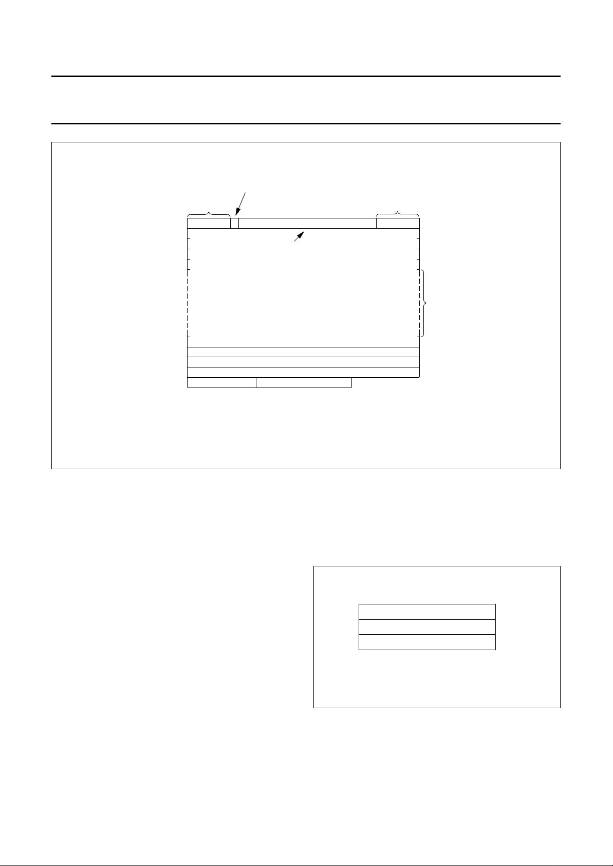
The acquired teletext packets each contain 40 bytes of
data and one packet is stored in each row of the text
memory. The page memory organization is given in Fig.5.
Rows 0 to 23 form the teletext page; Row 24 is available
for status messages and FLOF/FASTEXT prompt
information.
February 1995 24
Page 25
Philips Semiconductors Preliminary specification
One page Economy Teletext/TV
microcontroller
handbook, full pagewidth
7 characters
for status
10 bytes for
received
page information
hardware, alphanumerics white nor-
mally, alphanumerics green when
6178
24 characters from page header
rolling when display page looked for
MAIN PAGE DISPLAY AREA
PACKET X24 STORED HERE IF TXT0.7 = 1
10 14
fixed character written by
looking for display page
PACKET X / 22
PACKET X / 23
14 bytes
free for use
by microcontroller
8 characters
usually rolling
(time)
3931 32
MLC106
SAA5290
ROW
0
1
2
3
4
5
to
20
21
22
23
24
25
Fig.5 Basic page memory organization.
ROW 0 (see Fig.5)
Row 0 is for the page header. The first seven characters
(0 to 6) are free for status messages. Character 8 is an
alphanumeric white or green control character, written
automatically by SAA5290 to give a green rolling header
when a page is being looked for. The last eight characters
are for rolling time.
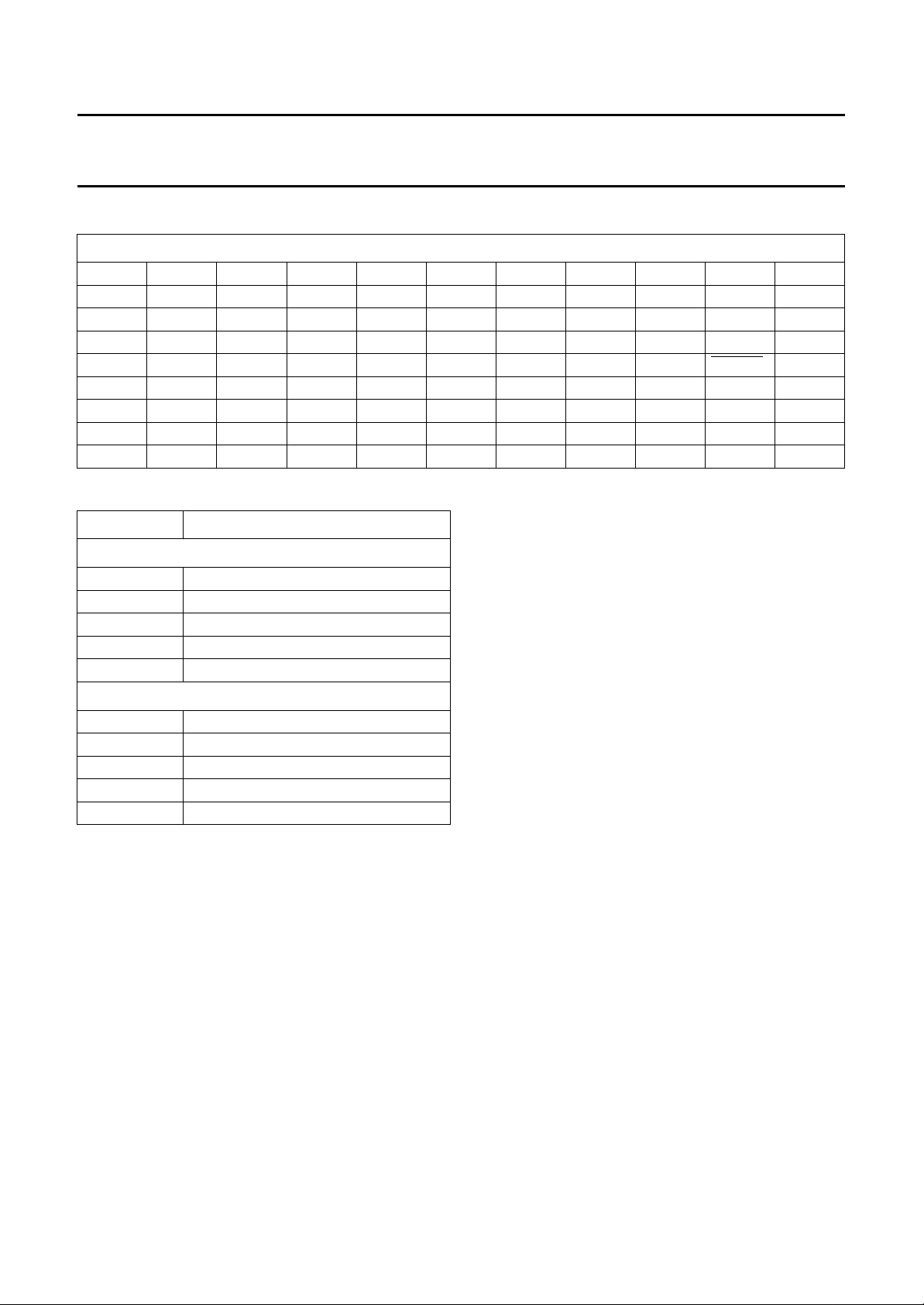
R
OW 25 (see Fig.5)
The first 10 bytes of row 25 contain control data relating to
the received page as shown in Table 14. The remaining 14
bytes are free for use by the microcontroller.
Extension packet memory organization
If TXT0.X24 POS bit is set to logic 0, then Packet 24 is
written into Row 0 of the extension memory.
Packet X27/0 is written to Row 1 of the extension memory,
with bytes 0 to 37 being Hamming checked automatically.
Packet 8/30 is written to Row 2 of the extension memory,
with bytes 0 to 6 being 8/4 Hamming checked, bytes
7 to 19 unchecked and bytes 20 to 39 odd parity checked.
Packet 26 processing
The SAA5290 contains on-board hardware processing of
Packet 26 data. If a character corresponding to that being
transmitted is available in the character set then the
correct character code is written into the display memory.
handbook, halfpage
PACKET X24 if TXT0.X24 POS = 0
PACKET X27 / 0
PACKETS 8 / 30 / 0 to 15
ROW
0
1
2
MLC107
Fig.6 Organization of the extension memory.
February 1995 25
Page 26
Philips Semiconductors Preliminary specification
One page Economy Teletext/TV
SAA5290
microcontroller
Table 14Row 25 received control data format
ROW 25
D0 PU0 PT0 MU0 MT0 HU0 HT0 C7 C11 MAG0 0
D1 PU1 PT1 MU1 MT1 HU1 HT1 C8 C12 MAG1 0
D2 PU2 PT2 MU2 MT2 HU2 C5 C9 C13 MAG2 0
D3 PU3 PT3 MU3 C4 HU3 C6 C10 C14 0 0
D4 HAM.ER HAM.ER HAM.ER HAM.ER HAM.ER HAM.ER HAM.ER HAM.ER
D5 0 0 0 0 0 0 0 0 0 PBLF
D60000000000
D70000000000
Column 0 1 2 3 4 5 6 7 8 9
Table 15Page number and sub-code for Table 14
BIT NAME DESCRIPTION
Page number
MAG magazine
PU page units
PT page tens
PBLF page being looked for
HAM.ER Hamming error in corresponding byte
FOUND 0
Page sub-code
MU minutes units
MT minutes tens
HU hours units
HT hours tens
C4 to C14 transmitted control bits
February 1995 26
Page 27

Philips Semiconductors Preliminary specification
One page Economy Teletext/TV
microcontroller
Display
The capabilities of the display are based on the
requirements of level 1 teletext, with some enhancements
for use with locally generated On-Screen Displays (OSD).
The display consists of 25 rows each of 40 characters,
with the characters displayed being those from
Rows 0 to 24 of the basic page memory. The page
memory stores 8-bit character codes which correspond to
260 displayable characters and 44 control codes, normally
displayed as spaces. Each character is defined by a matrix
12 pixels high and 10 pixels deep. When displayed each
pixel is 0.5 µs wide and 1 TV line, in each field, high.
The SAA5290 signals the TV display circuits to display the
RGB outputs of the SAA5290 rather than video picture by
setting VDS HIGH. The way in which this signal is switched
is controlled by the TXT5 and TXT6 SFRs. There are three
control functions: background on, text on and picture on.
There are separate bits for each function for inside and
outside teletext boxes and if the newsflash or subtitle bits
are set. This allows the software to configure the type of
display required. The effect of the combination of these
bits is given in Table 16. The
Register 6 control when the output is pulled LOW. This
output is intended to act on the TV display circuits to
reduce the contrast of the video display.
COR bits in Register 5 and
SAA5290
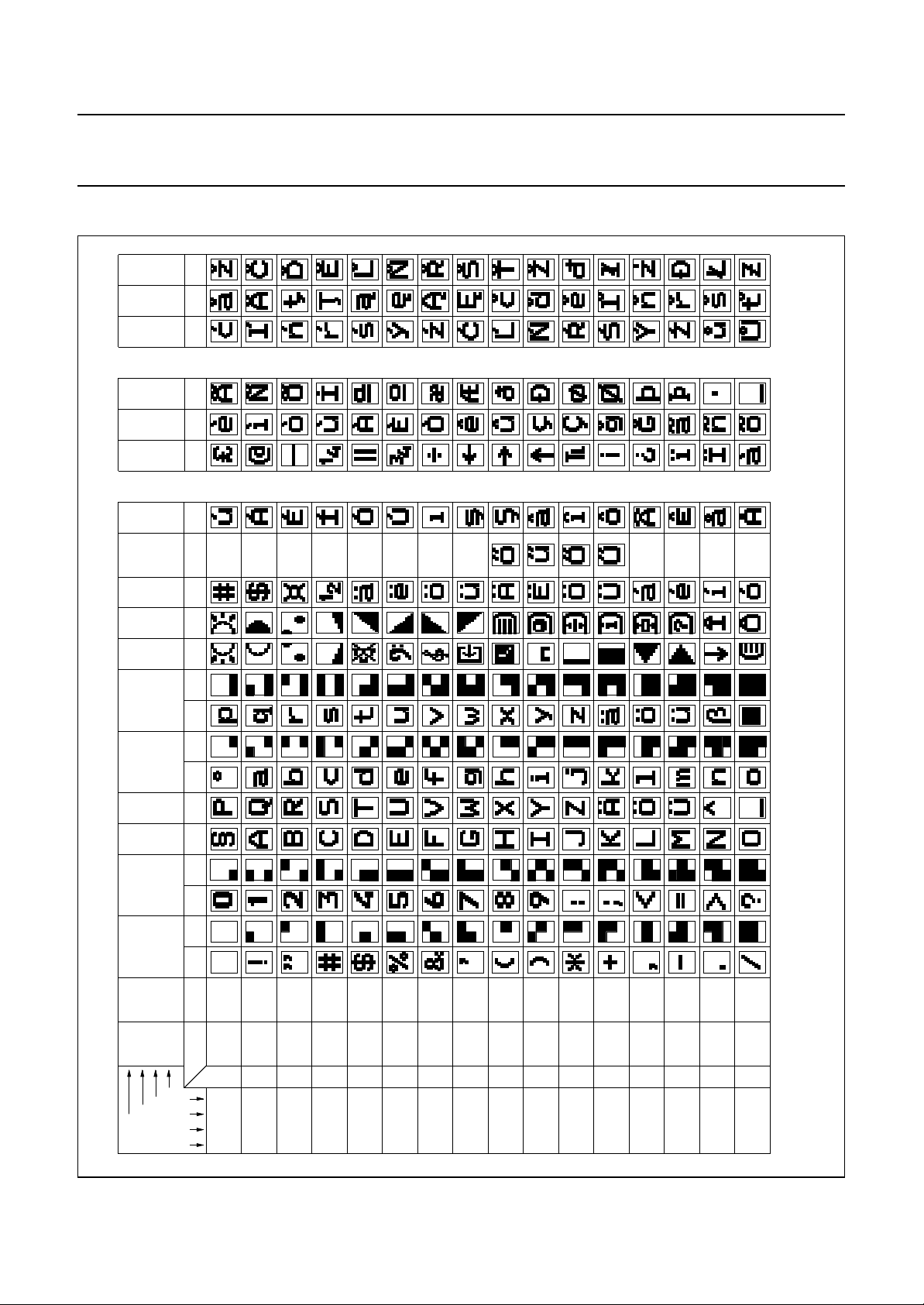
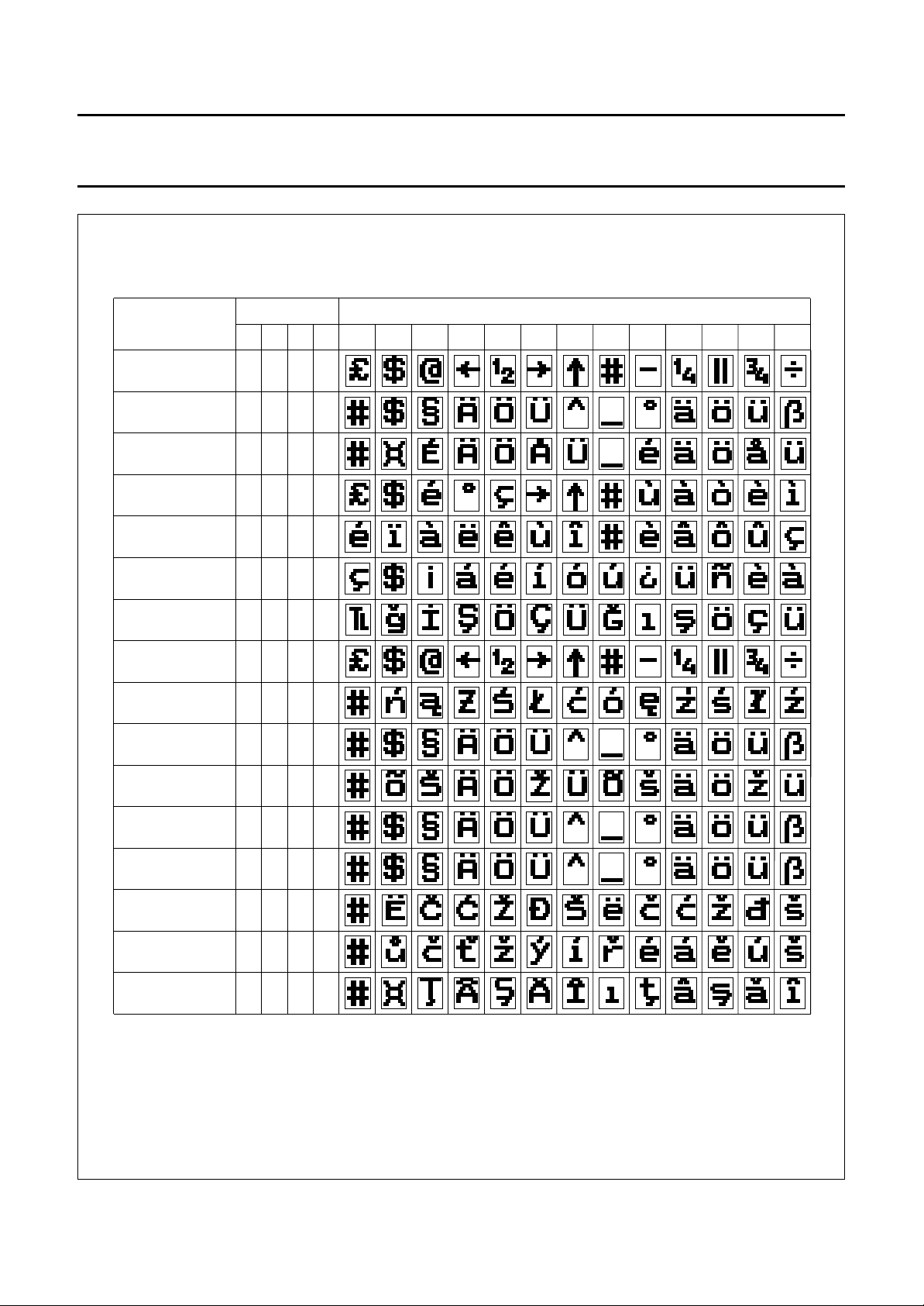
The display character set is given in Fig.9. The character
set provided contains all the characters required to display
Eastern and Western European languages. Register bit
TXT4.EAST/
languages are set with the C12 to C14 bits. In order to
make on-screen displays easy to use, the SAA5290
contains additional display attributes in Column 11.
Control codes are categorized as ‘set at’ or ‘set after’.
‘Set at’ means the code has effect at the current character
position and ‘set after’ means they have effect from the
following character. Codes 11/0 to 11/7 are always
‘set at’. Codes 11/11 to 11/15 are ‘set after’ when defining
the start of an OSD box and ‘set at’ when ending an OSD
box. Codes 11/12 to 11/15 force a box condition allowing
on-screen display messages to be displayed without
having to erase the whole contents of the teletext page.
On-screen displays are only available in TV mode and not
in text mode. In mixed text and TV mode the displayed
screen is not defined if an OSD box is encountered in the
page memory.
WEST sets whether Eastern or Western
Table 16 Display mode
PICTURE ON TEXT ON BACKGROUND ON RESULT
0 0 X text mode, black screen
0 1 0 text mode, background always black
0 1 1 text mode
1 0 X TV mode
1 1 0 mixed mode and TV mode
1 1 1 text mode, TV picture outside text area
Display timing
The display circuitry is driven from the H/VSYNC inputs,
and is independent of the input video signal. Consequently
HSYNC and VSYNC are always required to slave
synchronize the display.
The FRAME output of the SAA5290 is provided to facilitate
de-interlacing the teletext display. The behaviour of
FRAME is controlled via the register bits
TXT0.DISABLE FRAME, TXT0.AUTO FRAME and
TXT1.FIELD POLARITY. If the active edge of VSYNC
occurs in the first half of a TV line then the field is even, and
if the active edge of VSYNC is in the second half of a line
then the field is odd. The active edge is controlled with
TXT1.V POLARITY. With TXT0.AUTO FRAME LOW
FRAME is HIGH for an odd field and LOW for an even
field. With TXT0.AUTO FRAME HIGH FRAME is only
active when text is being displayed, when video is
displayed it is forced LOW. When TXT0.DISABLE FRAME
is HIGH FRAME is always LOW. If
TXT1.FIELD POLARITY is logic 1 then VSYNC is delayed
by 32 µs before being applied to the display timing circuits.
February 1995 27
Page 28
Philips Semiconductors Preliminary specification
One page Economy Teletext/TV
microcontroller
Clock generator
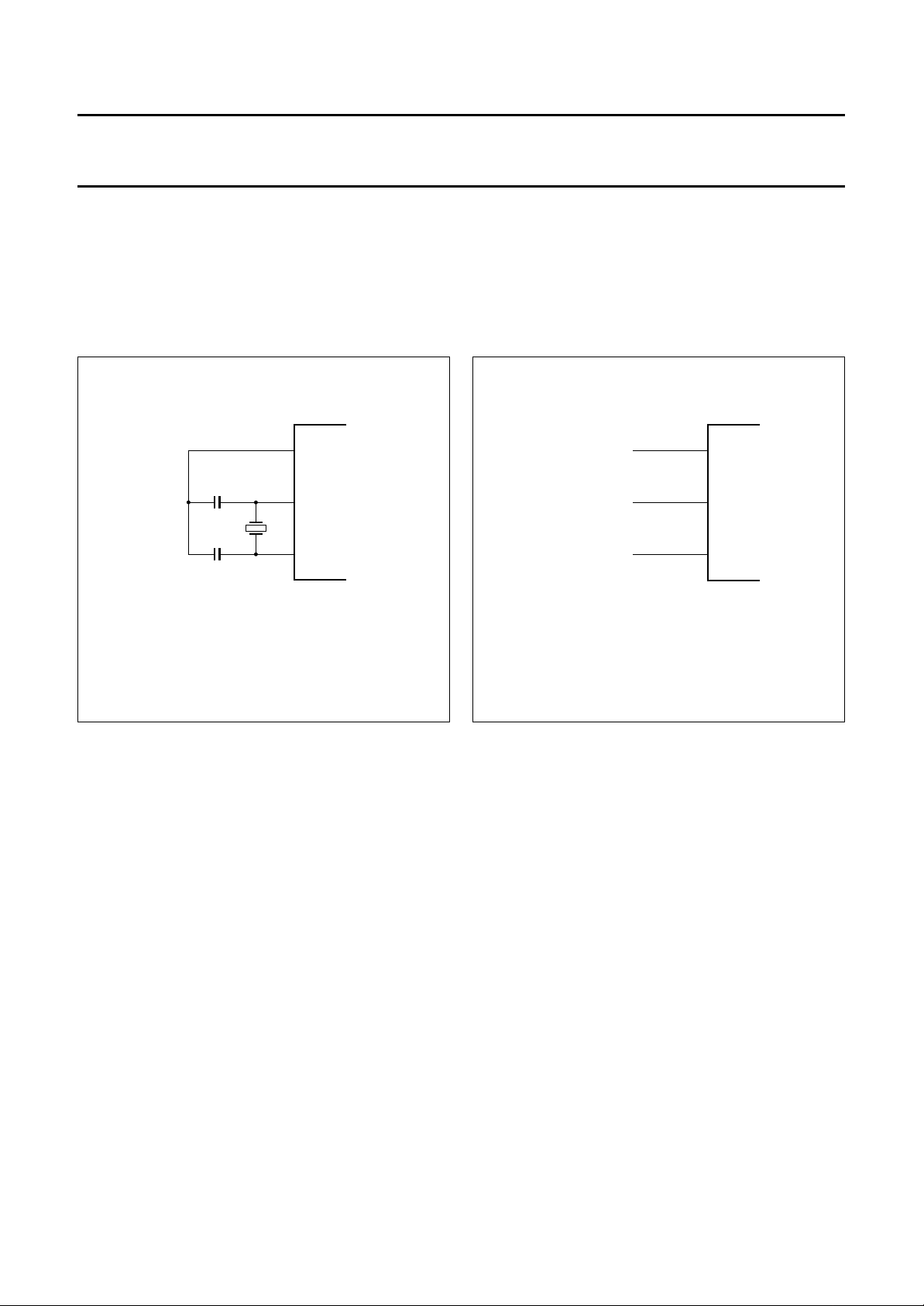
The oscillator circuit of the SAA5290 is a single-stage
inverting amplifier in a Pierce oscillator configuration. The
circuitry between OSCIN and OSCOUT is basically an
inverter biased to the transfer point. A crystal must be
used as the feedback element to complete the oscillator
handbook, halfpage
C1
C2
(1)
(1)
OSCGND
OSCIN
OSCOUT
MLC110
SAA5290
circuitry. It is operated in parallel resonance. OSCIN is the
high gain amplifier input and OSCOUT is the output. To
drive the SAA5290 externally OSCIN is driven from an
external source and OSCOUT is left open-circuit.
handbook, halfpage
not connected
external clock
not connected
OSCGND
OSCIN
OSCOUT
MLC111
(1) The values of C1 and C2 depend on the crystal specification:
C1 = C2 = 2C
.
L
Fig.7 Oscillator circuit.
Fig.8 Oscillator circuit driven from external source.
February 1995 28
Page 29
Philips Semiconductors Preliminary specification
One page Economy Teletext/TV
microcontroller
CHARACTER SETS
1
1
1
1
0
1
1
1
1
0
1
1
0
1
1
0
0
0
1
1
0
1
1
0
0
0
1
1
DEF
DEF
B
A
back-
black
ground
back
red
ground
back-
green
ground
back-
yellow
ground
1
1
1
1
1
1
1
1
1
1
0
1
0
1
0
1
0
1
1
0
back-
blue
ground
back-
ground
magenta
back-
cyan
ground
back-
white
ground
size
normal
OSD
height
double
OSD
width
double
OSD
SAA5290
MLC108
size
OSD
double
handbook, full pagewidth
0
1
1
0
1
0
1
0
0
0
1
0
1
1
0
0
0
1
0
0
1
0
0
0
0
0
0
0
6
b
7
b
I
T
B
0 1 22a3 3a4 5 66a77a8 9 C
alpha -
column
r
o
w
4
0
b
b
5
b
1
b
2
b
3
S
b
black
graphics
black
alpha -
numerics
0
0 0 0 0
red
graphics
red
numerics
10 0 0 1
green
graphics
green
alpha -
numerics
2
0 0 1 0
yellow
graphics
yellow
alpha -
numerics
30 0 1 1
blue
graphics
blue
alpha -
numerics
40 1 0 0
graphics
magenta
alpha -
magenta
numerics
5
0 1 0 1
cyan
graphics
cyan
alpha -
numerics
60 1 1 0
white
graphics
white
alpha -
numerics
70 1 1 1
display
conceal
flash
8
1 0 0 0
graphics
contiguous
91 0 0 1 steady
graphics
separated
A1 0 1 0 end box
B1 0 1 1 start box
black
back -
ground
height
normal
C1 1 0 0
new
back -
ground
height
double
D1 1 0 1
hold
graphics
width
double
E1 1 1 0
release
graphics
size
double
F1 1 1 1
Fig.9 SAA5290 European character set.
February 1995 29
Page 30
Philips Semiconductors Preliminary specification
One page Economy Teletext/TV
microcontroller
handbook, full pagewidth
LANGUAGE
ENGLISH
GERMAN
SWEDISH
ITALIAN
FRENCH
SPANISH
PHCB
E/W
C12 C13 C14
0
000
0
001
0
010
0
011
0
100
01
10
2 / 3
2 / 4 4 / 0
SAA5290
CHARACTER POSITION (COLUMN / ROW)
5 / B 5 / C 5 / D 5 / E 5 / F 6 / 0 7 / B 7 / C 7 / D 7 / E
TURKISH
ENGLISH
POLISH
SERBO-CROAT
CZECHOSLOVAKIA
RUMANIAN
1100
111
0
0010
001GERMAN 1
010ESTONIAN 1
011GERMAN 1
100GERMAN 1
101
1
110
1
11
11
MLC109
Fig.10 SAA5290 European national option characters.
February 1995 30
Page 31
Philips Semiconductors Preliminary specification
One page Economy Teletext/TV
microcontroller
APPLICATION INFORMATION
TV
control
signals
DD
V
kΩ
SCL
DD
DD
100
47
SDA
SS
V
4.7
P1.5
P1.4
nF
µF
P2.0/TPWM
P2.1/PWM0
P1.6/SCL
P1.7/SDA
P2.2/PWM1
P2.3/PWM2
P1.3/T1
P1.2/INT0
P2.4/PWM3
P2.5/PWM4
V
V
A0
EEPROM
PCF8582E
DD
RC
DD
A1
A2
V
V
IR
P1.1/T0
P1.0/INT1
P2.6/PWM5
P2.7
RECEIVER
DD
V
2.2 µF
DD
V
DDM
V
RESET
P3.0/ADC0
P3.1/ADC1
DD
V
OSCOUT
P3.2/ADC2
47
100
12 MHz
OSCIN
P3.3
µF
nF
OSCGND
SSD
V
V
DDT
V
P0.0
SAA5290
to TV's
circuits
G
P0.6
B
P0.7
display
DD
V
1
RGBREF
SSA
V
kΩ
3.3
10
kΩ
kΩ
100 nF
P3.4
CVBS0
COR
CVBS1
SSD2
V
BLACK
FRAME
IREF
MLC112
handbook, full pagewidth
27 kΩ
line flyback
field flyback
DD
R
VSYNC
VDS
HSYNC
DDA
V
SAA5290
P0.1
P0.2
P0.3
P0.4
P0.5
DD
V
PH2369
100 nF
100 nF
100
nF
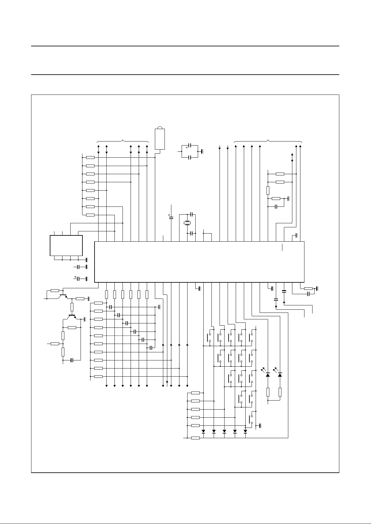
Fig.11 Typical application diagram.
CVBS (IF)
CVBS (SCART)
40 V
tune
V
DD
V
brightness
contrast
hue
saturation
volume (L)
volume (R)
afc
V
DD
V
1 kΩ
DD
V
February 1995 31
Page 32
Philips Semiconductors Preliminary specification
One page Economy Teletext/TV
microcontroller
PACKAGE OUTLINE
15.80
15.24
max
5.08
max
4.57
min
0.51
0.32 max
0.18 M
15.24
17.15
15.90
MSA267
14.1
SAA5290
13.7
47.92
47.02
3.2
seating plane
handbook, full pagewidth
2.8
max
0.53
1.778
max
1.73
(25x)
1.3 max
27
26
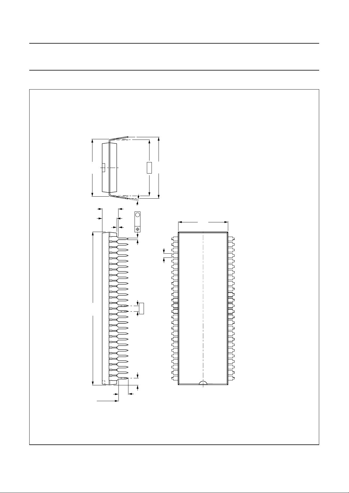
Fig.12 Plastic shrink dual in-line package; 52 leads (600 mil) SDIP52, SOT247-1.
52
1
February 1995 32
Dimensions in mm.
Page 33
Philips Semiconductors Preliminary specification
One page Economy Teletext/TV
SAA5290
microcontroller
SOLDERING
Plastic dual in-line packages
Y DIP OR WAVE
B
The maximum permissible temperature of the solder is
260 °C; this temperature must not be in contact with the
joint for more than 5 s. The total contact time of successive
solder waves must not exceed 5 s.
The device may be mounted up to the seating plane, but
the temperature of the plastic body must not exceed the
DEFINITIONS
Data sheet status
Objective specification This data sheet contains target or goal specifications for product development.
Preliminary specification This data sheet contains preliminary data; supplementary data may be published later.
Product specification This data sheet contains final product specifications.
Limiting values
Limiting values given are in accordance with the Absolute Maximum Rating System (IEC 134). Stress above one or
more of the limiting values may cause permanent damage to the device. These are stress ratings only and operation
of the device at these or at any other conditions above those given in the Characteristics sections of the specification
is not implied. Exposure to limiting values for extended periods may affect device reliability.
Application information
Where application information is given, it is advisory and does not form part of the specification.
specified storage maximum. If the printed-circuit board has
been pre-heated, forced cooling may be necessary
immediately after soldering to keep the temperature within
the permissible limit.
EPAIRING SOLDERED JOINTS
R
Apply the soldering iron below the seating plane (or not
more than 2 mm above it). If its temperature is below
300 °C, it must not be in contact for more than 10 s; if
between 300 and 400 °C, for not more than 5 s.
LIFE SUPPORT APPLICATIONS
These products are not designed for use in life support appliances, devices, or systems where malfunction of these
products can reasonably be expected to result in personal injury. Philips customers using or selling these products for
use in such applications do so at their own risk and agree to fully indemnify Philips for any damages resulting from such
improper use or sale.
2
PURCHASE OF PHILIPS I
C COMPONENTS
Purchase of Philips I
components in the I2C system provided the system conforms to the I2C specification defined by
Philips. This specification can be ordered using the code 9398 393 40011.
2
C components conveys a license under the Philips’ I2C patent to use the
February 1995 33
 Loading...