

Page 1

DATA SH EET
Preliminary specification
File under Integrated Circuits, IC02
1996 Oct 25
INTEGRATED CIRCUITS
SAA4970T
Economical video processing IC
(ECOBENDIC)
Page 2
1996 Oct 25 2
Philips Semiconductors Preliminary specification
Economical video processing IC
(ECOBENDIC)
SAA4970T
FEATURES
• Digital horizontal PLL
• Digital CTI (DCTI)
• Digital luminance peaking
• Digital phase compensation filter
• D/A conversion
• Simple multi picture processing
• Coloured frame generation
• Memory/sync processing.
GENERAL DESCRIPTION
The ECOBENDIC is an economical video processing IC
(Economical Back End IC) for double scan conversion.
It consists of sync/memory control, video enhancing
features and D/A conversion. The IC is designed to
cooperate with an 83C654 type of microcontroller,
Texas Instruments TMS4C2970/2971 memories plus a
4:1:1 A/D converter TDA8755/8753A.
QUICK REFERENCE DATA
ORDERING INFORMATION
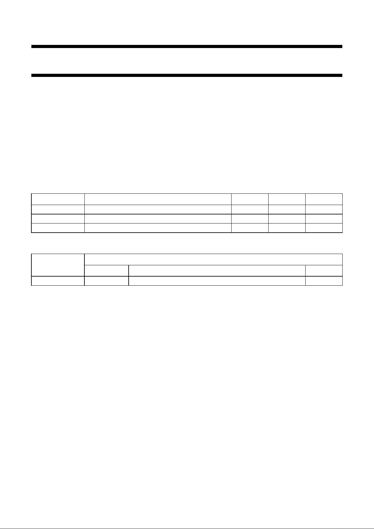
SYMBOL PARAMETER MIN. MAX. UNIT
V
DD
digital supply voltage 4.5 5.5 V
V
CC
analog supply voltage 4.75 5.25 V
T
amb
operating ambient temperature 0 70 °C
TYPE NUMBER
PACKAGE
NAME DESCRIPTION VERSION
SAA4970T VSO56 plastic very small outline package; 56 leads SOT190-1
Page 3
1996 Oct 25 3
Philips Semiconductors Preliminary specification
Economical video processing IC
(ECOBENDIC)
SAA4970T
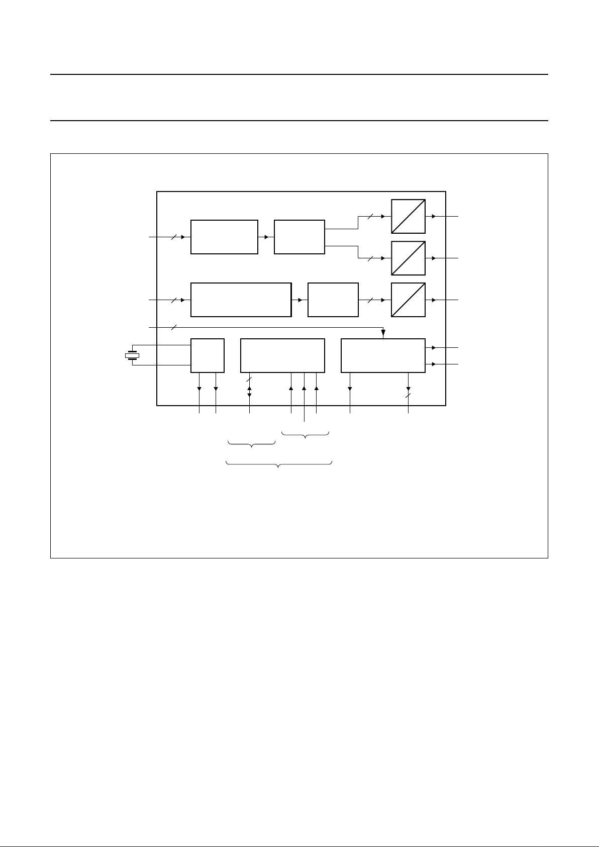
BLOCK DIAGRAM
Fig.1 Block diagram.
handbook, full pagewidth
MGE092
REFORMATTER
UP-SAMPLING
PHASE COMPENSATION
FILTER
MICROCONTROLLER
INTERFACE
SYNC PROCESSING
MEMORY CONTROL
DCTI
PLL
PEAKING
D
A
D
A
D
A
4
8
8
9
47 to
50
UVIN3
to UVIN0
8
2
8
3
53
CK1 CK2 ALE
WRN
RDN CLMP IE, WE, REmicrocontroller
parallel bus
AD7 to AD0
microcontroller
command
address line
microcontroller parallel bits
51
29 to 36
14
V
D
H
D
Y
O
V
O
U
O
19
7
5
3
18
15 to 17
24 27 28
37 to 41,
44 to 46
22, 23
55
56
SAA4970T
Xtal
O
Xtal
I
HA, V
A
YIN7
to YIN0
Page 4
1996 Oct 25 4
Philips Semiconductors Preliminary specification
Economical video processing IC
(ECOBENDIC)
SAA4970T
PINNING
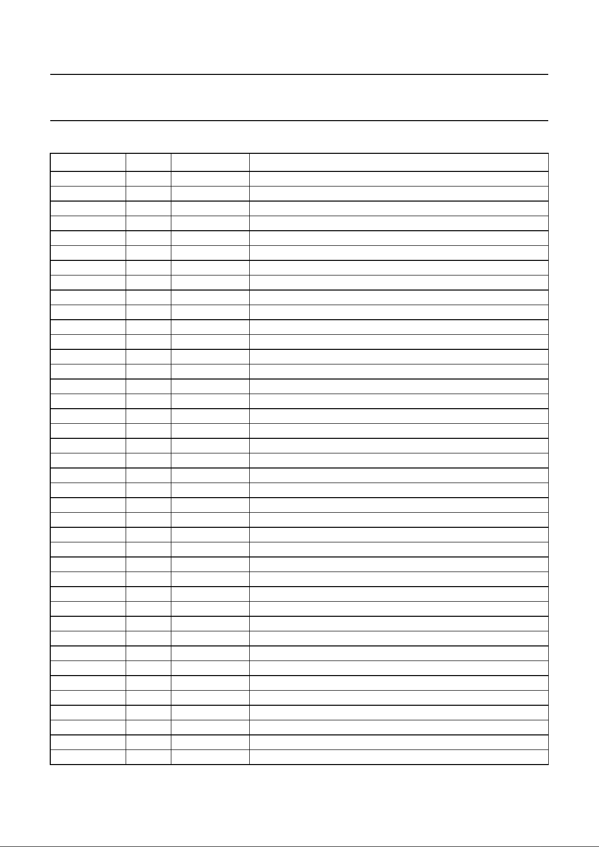
SYMBOL PIN TYPE DESCRIPTION
TEST2 1 input test control
P
mirref
2 input decoupling P-mirror reference
U
O
3 output analog U output
V
SSA
4 ground analog ground (0 V)
V
O
5 output analog V output
V
CC
6 supply analog supply voltage (+5 V)
Y
O
7 output analog Y output
V
ref
8 supply analog supply voltage reference D/A ladder HIGH
I
ref
9 supply reference current
V
refH
10 supply D/A decoupling capacitor
R1 11 I/O reset acquisition horizontal counter
R2 12 I/O reset display horizontal counter
PIP 13 input PIP related input 0
CLMP 14 output clamping control
IE 15 output field memory input enable
WE 16 output field memory write enable
RE 17 output field memory read enable
V
D
18 I/O display vertical pulse
H
D
19 output display horizontal pulse
RESET 20 output watchdog output (microcontroller reset)
BONE 21 input watchdog input (microcontroller bone)
H
A
22 I/O acquisition horizontal pulse
V
A
23 I/O acquisition vertical pulse
ALE 24 input address latch enable
IT1 25 output acquisition related interrupt
IT2 26 output display related interrupt
WRN 27 input write not pulse
RDN 28 input read not pulse
AD7 29 I/O programmable signal positioner (psp) data bus bit 7 (MSB)
AD6 30 I/O psp data bus bit 6
AD5 31 I/O psp data bus bit 5
AD4 32 I/O psp data bus bit 4
AD3 33 I/O psp data bus bit 3
AD2 34 I/O psp data bus bit 2
AD1 35 I/O psp data bus bit 1
AD0 36 I/O psp data bus bit 0 (LSB)
YIN7 37 input Y input bus bit 7 (MSB)
YIN6 38 input Y input bus bit 6
YIN5 39 input Y input bus bit 5
YIN4 40 input Y input bus bit 4
Page 5

1996 Oct 25 5
Philips Semiconductors Preliminary specification
Economical video processing IC
(ECOBENDIC)
SAA4970T
YIN3 41 input Y input bus bit 3
V
DD
42 supply digital supply voltage (+5 V)
V
SS
43 ground digital ground (0 V)
YIN2 44 input Y input bus bit 2
YIN1 45 input Y input bus bit 1
YIN0 46 input Y input bus bit 0 (LSB)
UVIN3 47 input UV input bus bit 3 (MSB)
UVIN2 48 input UV input bus bit 2
UVIN1 49 input UV input bus bit 1
UVIN0 50 input UV input bus bit 0 (LSB)
CK2 51 I/O display clock
V
SS
52 ground digital ground (0 V)
CK1 53 I/O acquisition clock
TEST1 54 input test control
Xtal
O
55 output external crystal output (12 MHz)
Xtal
I
56 input PLL crystal input (12 MHz)
SYMBOL PIN TYPE DESCRIPTION
Page 6
1996 Oct 25 6
Philips Semiconductors Preliminary specification
Economical video processing IC
(ECOBENDIC)
SAA4970T
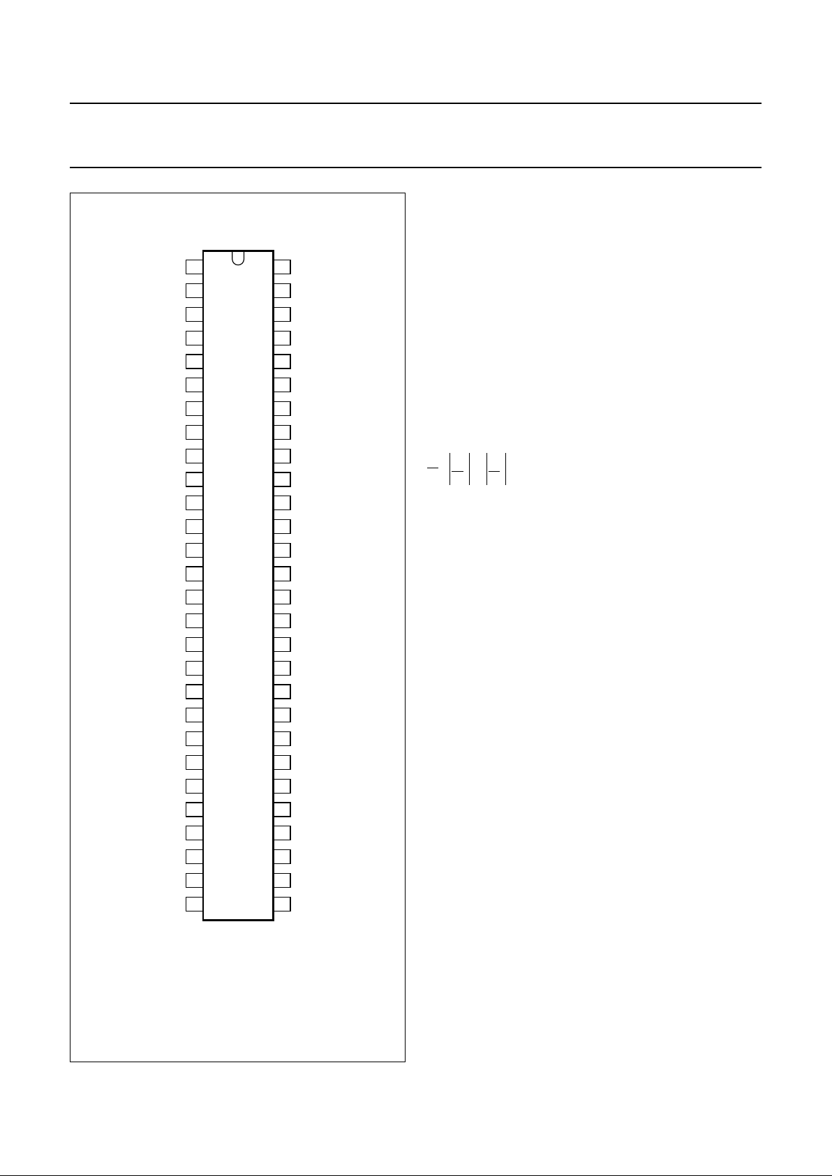
Fig.2 Pin configuration.
handbook, halfpage
SAA4970T
MGE091
1
2
3
4
5
6
7
8
9
10
11
12
13
14
15
16
17
18
19
20
21
22
23
24
25
26
52
51
50
55
56
54
53
49
48
47
46
45
44
43
42
41
40
39
38
37
36
35
34
33
32
31
30
29
TEST2
P
mirref
U
O
V
SSA
V
O
V
CC
Y
O
V
ref
I
ref
V
refH
R1
R2
PIP
CLMP
IE
WE
RE
V
D
H
D
RESET
BONE
H
A
V
A
ALE
IT1
IT2
Xtal
I
Xtal
O
TEST1
CK1
V
SS
CK2
UVIN0
UVIN1
UVIN2
UVIN3
YIN0
YIN1
YIN2
V
SS
V
DD
YIN3
YIN4
YIN5
YIN6
YIN7
AD0
AD1
AD2
AD3
AD4
AD5
27
28
WRN
RDN
AD6
AD7
FUNCTIONAL DESCRIPTION
ECO data path
The data path performs the DCTI, peaking, phase
compensation, framing and blanking functions plus colour
reformatting and variable delay of Y to UV at the input and
output of the data path.
DCTI
DCTI is implemented to get a dynamic interpolation of the
low bandwidth U and V signals. First a 2 : 1 linear
interpolation is done, to go from a 4 :1:1 format to a
4:2:2 format. A second interpolation is done in which the
data path delay is varied on the basis of a function of the
second derivative of the U and V signal (or more precise:
). The effect at an edge is that during the
first half the data path delay is higher than nominal and in
the second half it is lower than nominal. This will make the
edge much steeper. As this second interpolation is done
with the resolution equal to that of the Y samples and also
with a zero DCTI gain a 2 : 1 interpolation is performed, a
4:4:4 format is obtained.
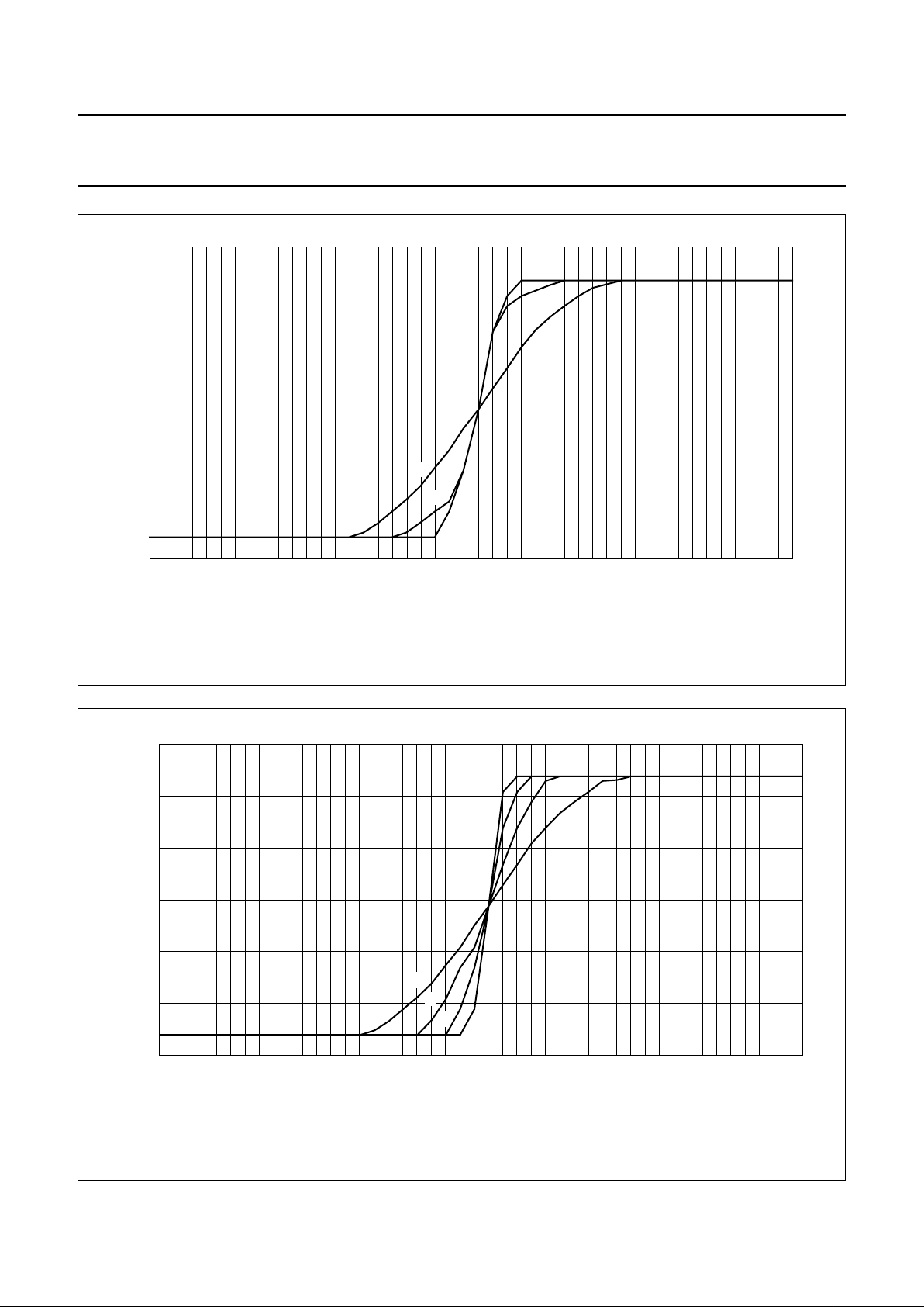
The DCTI function can be controlled by setting the range
to ±12, ±8, ±6 or ±4 pixels (see Fig.3) or by adjusting the
gain to 0,
1
⁄4,1⁄2 or 1.
An artefact of this processing exists when two edges are
close together in the video. During the second half of the
first edge a delay is chosen that will collect video data
where the second edge is already active. The same is valid
for the second edge. The result of this processing on a
video pulse, which is looking like a hill, is that of a hill with
one or two bumps in it. To prevent this from happening, the
positions where the first derivatives in U and V change
sign, are marked and used to limit the range of the relative
delay. This function is called ‘over the hill protection’. It can
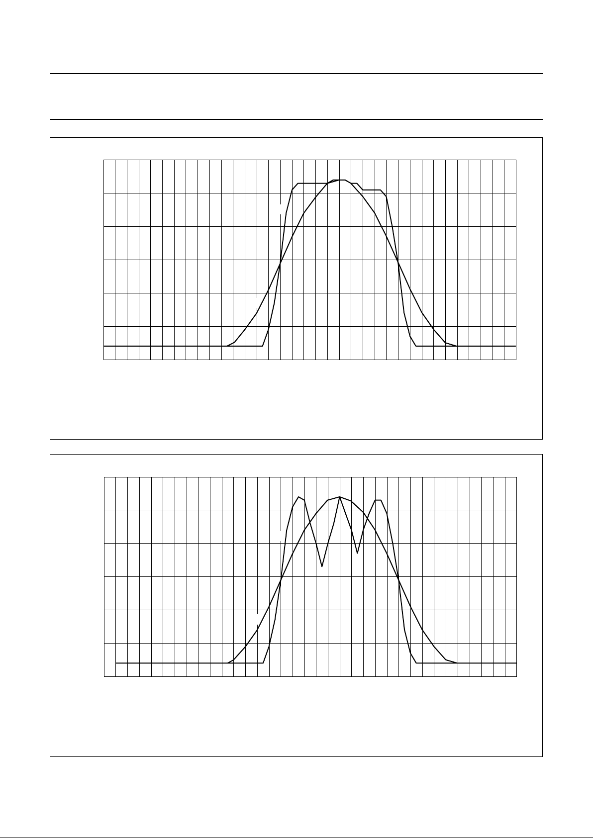
be turned on and off. Figures 5 and 6 show the effect of
the DCTI function with and without ‘over the hill protection’
when applied to a hill-shaped video pulse.
td
d
td
dUtddV
+{}
Page 7
1996 Oct 25 7
Philips Semiconductors Preliminary specification
Economical video processing IC
(ECOBENDIC)
SAA4970T
handbook, full pagewidth
120
digital
signal
amplitude
100
80
60
110
samples
40 45352515530
MGE093
20
(1)
(2)
(3)
Fig.3 DCTI with variation of k range.
(1) input signal.
(2) range = 4.
(3) range = 12.
Gain =1⁄2.
Fig.4 DCTI with variation of k gain.
(1) input signal.
(2) gain = 0.25.
(3) gain = 0.5.
(4) gain = 1.
Range = 12.
handbook, full pagewidth
120
digital
signal
amplitude
100
80
60
110
samples
40 45352515530
MGE094
20
(1)
(2)
(3)
(4)
Page 8
1996 Oct 25 8
Philips Semiconductors Preliminary specification
Economical video processing IC
(ECOBENDIC)
SAA4970T
Fig.5 DCTI with ‘over the hill protection’.
Gain =1⁄2.
Range = ±12.
Hill protection = on.
(1) output.
(2) input.
handbook, full pagewidth
120
digital
signal
amplitude
100
80
60
20 30 90
samples
807060
MGE095
5040
(1)
(2)
Fig.6 DCTI without ‘over the hill protection’.
handbook, full pagewidth
120
digital
signal
amplitude
100
80
60
20 30 90
samples
807060
MGE096
5040
(2)
(1)
Gain =1⁄2.
Range = ±12.
Hill protection = off.
(1) output.
(2) input.
Page 9
1996 Oct 25 9
Philips Semiconductors Preliminary specification
Economical video processing IC
(ECOBENDIC)
SAA4970T
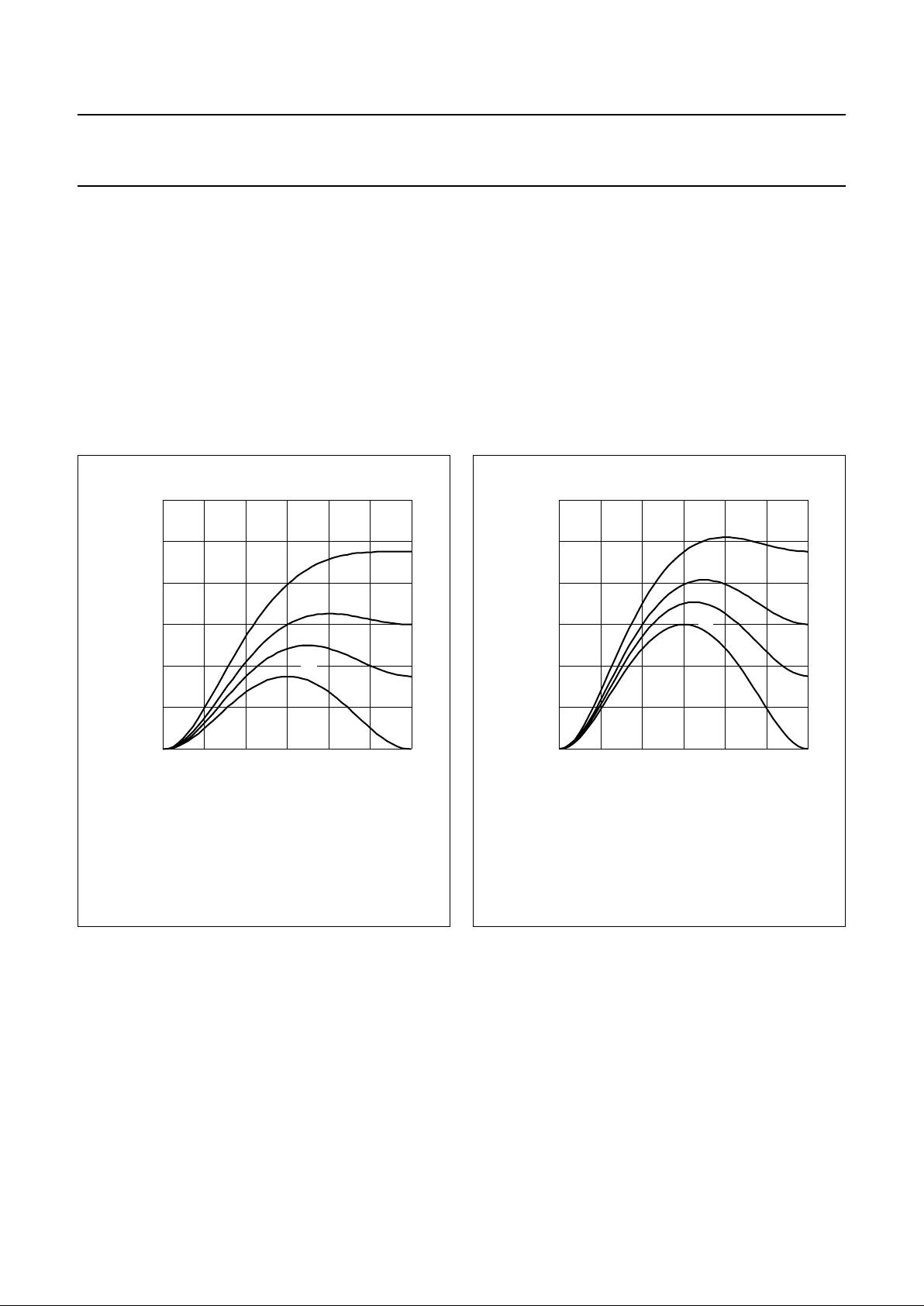
PEAKING
Peaking is implemented to obtain a higher gain in the
middle and upper ranges of the luminance bandwidth.
The filtering is an addition of:
• the original signal
• the original signal band-passed with centre
frequency =1⁄4f
s
• the original signal high-passed with maximum gain at
frequency =1⁄2fs.
The band-passed and high-passed signals are weighted
with factors 0,
1
⁄8,1⁄4 and1⁄2. The impulse response
becomes [−α, −β, 1 + 2α +2β,−β, −α], where α is the
band-pass weighting factor and β the high-pass weighting
factor.
Coring is added to obtain no gain for low amplitudes in the
(high-pass + band-pass) signal, which is then considered
to be noise. Coring levels can be programmed as 0 (off),
+1/−2, +3/−4 and +7/−8 LSB at 10-bit word.
A limiter brings back the 11-bit range to a 9-bit range with
a clipping function on the lower and upper side.
Fig.7 Peaking transfer function with variation of β
(α =1⁄8).
(1) β =1⁄2.
(2) β =1⁄4.
(3) β =1⁄8.
(4) β =0.
handbook, halfpage
0
0
2
4
6
8
10
12
1/4f
s
1/2f
s
MGE097
IH_PeakingI
(dB)
(1)
(2)
(3)
(4)
Fig.8 Peaking transfer function with variation of β
(α =1⁄4).
(1) β =1⁄2.
(2) β =1⁄4.
(3) β =1⁄8.
(4) β =0.
handbook, halfpage
0
0
2
4
6
8
10
12
1/4f
s
1/2f
s
MGE098
IH_PeakingI
(dB)
(1)
(2)
(3)
(4)
Page 10
1996 Oct 25 10
Philips Semiconductors Preliminary specification
Economical video processing IC
(ECOBENDIC)
SAA4970T
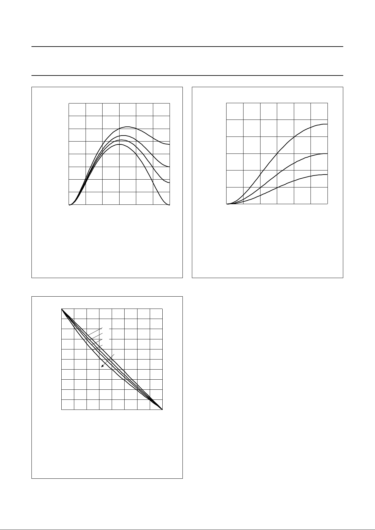
Fig.9 Peaking transfer function with variation of β
(α =1⁄2).
(1) β =1⁄2.
(2) β =1⁄4.
(3) β =1⁄8.
(4) β =0.
handbook, halfpage
0
0
2
4
6
8
10
12
14
16
1/4f
s
1/2f
s
MGE099
IH_PeakingI
(dB)
(1)
(2)
(3)
(4)
Fig.10 Peaking transfer function with variation of β
(α = 0).
(1) β =1⁄2.
(2) β =1⁄4.
(3) β =1⁄8.
handbook, halfpage
0
0
2
4
6
8
10
12
1/4f
s
1/2f
s
MGE100
IH_PeakingI
(dB)
(1)
(2)
(3)
PHASE COMPENSATION
Fig.11 Phase spectrum of NLP filter transfer
function.
(1) λ =0.
(2) λ =1⁄8.
(3) λ =1⁄4.
(4) λ =1⁄2.
handbook, halfpage
0 0.125 0.25 0.5
0
MGE101
0.375
−1/2
π
− π
Φ
nlp
(f/fs)
f/f
s
(1)
(2)
(3)
(4)
To compensate for a non-linear phase characteristic
before the A/D converter, this filter will compensate such
behaviour with a pulse response of [−λ, 1 + λ]. λ can be
programmed for the values 0,1⁄8,1⁄4 and1⁄2.
An 8-bit word width is re-obtained by means of clipping at
0 and 255.
F
RAMING AND BLANKING
Blanking is done with switching Y to value 16 and UV to
value 0 (in twos complement) on command of the BL
signal.
Framing is done by switching Y and the higher nibble of U
and V to certain programmable values (frame Y and
frame UV) on command of the signal KAD.
If the pixel repetition function is chosen the last values from
the video remain repeated instead of the fixed values.
The range of the output signal YO can be selected between
8 and 9 bits. In case of 8 bits for the nominal signal there
is room left for under and overshoot (adding up to a total of
9 bits); in case of selecting all 9 bits of the luminance D/A
converter for the nominal signal any under or overshoot
will be clipped.
Page 11

1996 Oct 25 11
Philips Semiconductors Preliminary specification
Economical video processing IC
(ECOBENDIC)
SAA4970T
VARIABLE INPUT AND OUTPUT DELAYS
To obtain flexibility, a programmable delay difference
between Y and UV can be made at both input and output.
At the input an almost symmetrical range of Y to UV delay
can be made: −3 to +4 clock pulses.
At the output a range of Y to UV delay from −5 to +2 clock
pulses can be made. When using e.g. scavenge circuitry,
which has an additional external delay, the lower delays in
Y are able to compensate this.
C
OLOUR REFORMATTING
The reformatter changes the DMSD 4 : 1 : 1 format UV
signals into a sequential 8-bit U and V format according to
the following scheme:
input:
U7, U5, U3, U1, U7, U5...etc.
U6, U4, U2, U0, U6, U4...etc.
V7, V5, V3, V1, V7, V5...etc.
V6, V4, V2, V0, V6, V4...etc.
output:
U7, V7, U7, V7...etc.
U6, V6, U6, V6...etc.
U5, V5, U5, V5...etc.
U4, V4, U4, V4...etc.
U3, V3, U3, V3...etc.
U2, V2, U2, V2...etc.
U1, V1, U1, V1...etc.
U0, V0, U0, V0...etc.
If the master clock frequency in the IC is 27 MHz then the
data rate of the reformatter output is 13.5 MHz.
The signals UVbin and UV8bit, supplied by the
microcontroller interface, select binary/twos complement
mode and 8-bit/7-bit operation.
Economy Controller - Programmable Signal
Positioner (ECO-PSP) control/microcontroller
interface and sync processing
The control/microcontroller interface and sync processing
part is designed as a separate unit called the ECO-PSP.
H
ORIZONTAL AND ACQUISITION BLOCK
CNT_A is an 8-bit counter, which counts up to
256 positions per acquisition video line. The cycle length
of the counter is determined by either:
an external reset (rising edge of R1) on every line or
an internal reset, generated at a certain value of the
counter itself.
For operation with the internal reset only, a value N in the
‘reset CNT_A’ register will result in an N + 1 length cycle.
The R1 signal, generated by the ECO-PLL, should then be
kept at a constant level. This however has not been
foreseen in the ECO-PLL, so this mode of operation is not
implied.
For operation with the external reset only, the ‘reset
CNT_A’ register must be loaded with a value above the
maximum line length. A value of FFH is suggested.
The VI1 input signal is monitored on its rising edge, with
regard to the CNT_A momentary value. By reading out
MUXA the positions of the edge becomes available for the
microcontroller. If VI1 is the video field pulse, the position
of the active edge within a video line becomes available.
This indicates the interlace situation of the acquisition
video signal. A window for discrimination of undesired VI1
edges is used. This window is made in the vertical
acquisition block.
If a write to ‘SAMPLE AQUI and DISPL’ is done, MUXA will
be loaded with the momentary CNT_A contents.
The PIP input signal is monitored on its edges, with regard
to the CNT_A momentary values. If the PIP interrupt is
enabled, an occurring rising edge will generate acquisition
interrupt. By reading out MUXF and MUXG, the positions
of the rising and falling edges become available for the
microcontroller.
The internal acquisition gate pulses GA1, GA2 and GA3
(routed to CLMP, WE and IE) are set and reset at
selectable CNT_A values. The sets of GA2 and GA3 have
to be enabled by the vertical acquisition block. If the set
and reset registers have equal contents, the signal will
remain reset (reset overruling set).
The internal acquisition horizontal pulse HI is HIGH when
the CNT_A contents are equal to a programmable value in
the HI position register.
Page 12

1996 Oct 25 12
Philips Semiconductors Preliminary specification
Economical video processing IC
(ECOBENDIC)
SAA4970T
VERTICAL ACQUISITION BLOCK
CNT_B is a 9-bit counter, which counts to up to 512 lines
per acquisition video field. The cycle length of the counter
is determined by either:
an external reset (rising edge of VI1) on every field or
an internal reset, generated at a certain value of the
counter itself, at the moment that the window is closed,
without a VI1 rising edge having occurred during the
window.
The counter value of CNT_B is monitored at the moment
the VI1 rising edge is detected and can be read out from
MUXB by the microcontroller. This value then indicates the
number of lines in a video field. If the window is closed,
without a VI1 rising edge having occurred during the
window, MUXB will also be filled with the momentary
contents of CNT_B.
If a write to ‘SAMPLE AQUI and DISPL’ is done, MUXB will
be loaded with the momentary CNT_B contents.
An interrupt can be generated on a pre-defined acquisition
line (Counter B-interrupt-Acquisition-b) by writing its line
number to the ‘set CB_intAb’ register. If the interrupt is not
desired, the register should be filled with a value above the
‘reset window’ register contents. The value 1FFH is
suggested. Otherwise the interrupt may be disabled by
bit 1 of the PLL control register (address 3D).
CNT_C is a 9-bit counter that resets to 0 at a pre-defined
state of CNT_B. The internal ‘Gate Enable’ signal is then
also set. ‘Gate Enable’ is reset at a pre-defined value of
CNT_C. At that moment also an interrupt can be
generated. If the interrupt is not desired, it can be disabled
by bit 3 in the PLL control register.
H
ORIZONTAL DISPLAY BLOCK
CNT_F is an 8-bit counter, which counts up to
256 positions per display video line. The cycle length of the
counter is determined by either:
an external reset or a reset from the ECO-PLL (rising
edge of R2) on every line or
an internal reset, generated at a certain value of the
counter itself.
For operation with the internal reset only, a value N in the
‘reset CNT_F’ register will result in an N + 1 length cycle.
The R2 input should now be kept HIGH or LOW. This
means in the ECOBENDIC the R2 output from the
ECO-PLL 3-state and the R2 signal will externally be kept
HIGH or LOW.
For operation with the external reset only, the ‘reset
CNT_F’ register must be loaded with a value above the
maximum line length. A value of FFH is suggested.
Whenever CNT_F is reset, the internal display horizontal
pulse HU is generated.
The signals BL, H2, KAD and internally GD (which
becomes RE in the gates block) have programmable sets
and resets, and can therefore have rising and falling edges
at any desired CNT_F value. If the set and reset registers
have equal contents, the signal will remain reset (reset
overruling set). To keep the signals set, the reset register
should remain above the maximum CNT_A value, while
the set value is within the CNT_A cycle range. The GD has
two pairs of set/reset registers, and can generate 4 edges
per line instead of 2. The KAD has three pairs of set/reset
registers, and can generate 6 edges per line instead of 2.
The GD pulse has a programmable fine shift of 0, 1, 2 or
3 CK2 pulses on both of its edges.
All the horizontal display output signals have enables on
the sets and resets. These enables will be effectively
changed only at the occurrence of the internal horizontal
HU pulse. Therefore it is possible to set up various signal
edges slowly by the microcontroller and effectuate them all
at once in a certain video line.
The VI2 input/output signal is monitored on its rising edge,
with regard to the CNT_F momentary value. By reading
out MUXD, the position of the edge becomes available for
the microcontroller. If VI2 is the video field pulse, the
position of the active edge within a video line becomes
available. This indicates the interlace situation of the
display video signal.
If a write to ‘SAMPLE AQUI and DISPL’ is done, MUXD will
be loaded with the momentary CNT_F contents.
If VI2 is used as an output, the ‘VHU register/comparator’
generates a line frequent pulse that is used in the vertical
display block for the timing of the VI2 edges within the
lines.
V
ERTICAL DISPLAY BLOCK
CNT_D is a 9-bit counter, which counts to maximum
512 lines per display video field. The cycle length of the
counter is determined by a reset action from the
microcontroller, i.e. writing to address 14H.
The counter value of CNT_D is monitored at the moment
the VI2 rising edge is detected and can be read out from
MUXE by the microcontroller. This value then indicates the
number of lines in a video field.
Page 13

1996 Oct 25 13
Philips Semiconductors Preliminary specification
Economical video processing IC
(ECOBENDIC)
SAA4970T
If a write to ‘SAMPLE AQUI and DISPL’ is done, MUXE will
be loaded with the momentary CNT_D contents.
An interrupt can be generated on a pre-defined display line
(Counter D-interrupt-Display-b) by writing its line number
to the ‘set CD_intDb’ register. If the interrupt is not desired,
the register should be filled with a value above the
maximum number of display lines. The value 1FFH is
suggested.
If VI2 is used as an output, the falling edge can be
activated by addressing the ‘start flyback’ register and the
rising edge by addressing the ‘start scan’ register. In the
‘horizontal display block’ a pulse is generated with the
‘VHU register/comparator’. This pulse is used for the
timing of the edges within the lines. This gives the ability to
determine the interlace of the display and is continuously
variable. It is useful to use the display interrupt to trigger
the microcontroller for issuing the flyback and scan edges
in a certain display line.
G
ATES BLOCK
The internal signals ‘Gate Acquisition 1’ (GA1), ‘Gate
Acquisition 2’ (GA2), ‘Gate Acquisition 3’ (GA3) and ‘Gate
Display’ (GD) are fed through shift stages, which are
programmed to shift the rising and falling edges 0, 1, 2 or
3 input clock periods. For GA1, GA2 and GA3 the shift is
in CK1 periods; for GD the shift is in CK2 periods.
The construction of the shifts makes it possible to generate
the gate outputs with higher resolution than the other
signals. If MC1 =1⁄4CK1 and MC2 =1⁄4CK2, any position
of the edges is possible with a resolution of CK1 and CK2
clock period.
A
CQUISITION AND DISPLAY INTERRUPTS BLOCKS
As described in the acquisition and display vertical blocks,
on programmed positions of CNT_B, CNT_C and CNT_D
interrupts are generated. Also, as described in the
horizontal acquisition block, an interrupt may be generated
on a rising edge of the PIP signal.
The PIP related interrupt and the ‘gate input, CNT_C’
related interrupt can be enabled or disabled by bits in the
PLL control register.
The status of each interrupt is separately held in a flip-flop.
The interrupt status flip-flops can all be monitored by
reading MUXC.
To reset any of the interrupts, the flip-flops can be reset
individually by addressing their reset interrupt address.
The interrupts are grouped into two output signals: IT1 is a
combination of all acquisition related interrupts, while IT2
is the only display related interrupt.
A
CQUISITION AND DISPLAY CLOCK BLOCKS
The CK1 and CK2 input clock signals are divided into div1
or div4 signals (internal clock signals), where div1 in only
meant for testing purposes. The divided clocks are
multiplexed to MC1 and MC2.
The multiplexer select states for MC1 and MC2 are
programmed in the internal control register.
M
ICROCONTROLLER INTERFACE BLOCK
The microcontroller interface consists of an addressing, a
read and a write part.
The addressing is performed with an address latch, that
latches the address/data bus while ‘address latch enable’
is active (HIGH).
Writing data to any destination in the ECO-PSP consists
of two activities:
1. The address in the address latch is converted to an
enable signal for the destination in question. This
enable is activated while WRN is active (LOW).
2. The 8-bit data on the address/data bus is merged with
a 9th bit, which is the highest bit (bit 7) of the address
latch. This resulting 9-bit data is sent to registers in the
various blocks. Most registers only use 8 bits of data,
in that case the 9th bit is a ‘don’t care’.
Writing to 7 addresses simultaneously is possible by
supplying an address in the range of 00H to 07H. All the
destinations in the column of that address in the write table
are then supplied with the same data.
The destinations in the ECO-PSP may be: 9-bit registers,
8-bit registers, counter resets, interrupt resets, gate output
selects and the acquisition and display function.
Reading data from one of the 7 readable registers also
consists of two activities:
1. The address in the address latch is converted to a
multiplexer setting for the source in question.
2. The 8-bit data from the source 3-state enabled to the
address/data bus. If a 9-bit register is read out, the
highest bit (bit 8) is coded in the MUXC source.
The seven sources in the ECO-PSP are described in the
read table.
Page 14

1996 Oct 25 14
Philips Semiconductors Preliminary specification
Economical video processing IC
(ECOBENDIC)
SAA4970T
ECO-PLL
In the PLL block, 3 functions are performed with the
following sub-blocks:
• Crystal oscillator
• PLL core
• Clock and R1 divider for multi picture.
C
RYSTAL OSCILLATOR
The crystal oscillator should drive an external 12 MHz
crystal used in the watchdog and externally by e.g. the
microcontroller.
PLL
CORE
In the PLL core, line locked clocks are made for both the
acquisition and display sides of the double scan
conversion circuits. The PLL can lock its outputs to an
externally applied Hs 16 kHz line pulse. The outputs are:
• CK2, the display clock
• CL1, the (basic) acquisition clock
• R2, the display 32 kHz line frequent pulse
• RL1, the (basic) 16 kHz line frequent pulse.
The CK2 frequency relates to the Hs frequency with a
factor determined by PLL_div:
PLL_div = 0 → CK2 = 2 × 1024 × Hs (nominal 32 MHz)
PLL_div = 1 → CK2 = 2 × 864 × Hs (nominal 27 MHz)
PLL_div = 2 → CK2 = 2 × 768 × Hs (nominal 24 MHz)
PLL_div = 3 → CK2 = 2 × 648 × Hs
(nominal 20.25 MHz).
The Cp and Ci settings in the PLL2 control byte correspond
to coefficients in the proportional and integrating parts of
the PLL control loop.
The actual proportional coefficient is 2
−(Cp + 1)
. With C
p
ranging from 0 to 7, 2
−(Cp + 1)
ranges from1⁄2to1⁄
256
.
The actual integrating coefficient is 2
−(Ci+2)
. With C
i
ranging from 0 to 15, 2
−(Ci+2)
ranges from1⁄4to1⁄
131072
.
The PLL core itself is driven by the 12 MHz signal from the
crystal oscillator.
The PLL can be set to lock upon the Hs signal, or to run
free at a fixed frequency or at the last frequency during
lock.
In normal operation the PLL locks to the Hs signal.
The win_PLL signal from the PSP part of the ECOBENDIC
windows the part of the picture where a VCR phase
disturbance might occur. This is normally part of the
vertical blanking period, but with the double scan
conversion and a single acquisition/display clock system,
it would become visible in the lower part of the picture as
bottom flutter. Therefore, with win_PLL active, the
frequencies generated by the PLL remain fixed at the last
frequencies during lock.
When the control bit ‘free run’ is active, a fixed frequency
will be produced, determined by the setting of PLL_div.
PLL_div = 0 gives 32 MHz, PLL_div = 1 gives 27 MHz,
PLL_div = 2 gives 24 MHz and PLL_div = 3 gives
20.25 MHz on the display clock CK2.
C
LOCK AND R1 DIVIDER FOR MULTI PICTURE
To make simple multi picture processing, it is possible to
reduce the clock rate at the acquisition side by a
factor 2 or 3.
Suppose, a factor of 3 is chosen. Then,1⁄3 of the memory
data that is normally written by 1 line of video will now be
written by 3 lines of the input video. If writing to the
memory is only enabled for a chosen1⁄3 of this period, a
desired part of the video line to be displayed is updated
with a compressed line of input video. After a cycle of
3 input lines, the write pointer of the memory is located on
a position, that will be displayed exactly 1 line below. For
this essential cycle of 3 input lines, also the 16 kHz RL1
pulse must be frequency divided by 3.
U
SE OF INTERNAL AND EXTERNAL PLL CIRCUITS
The ECOBENDIC is designed primarily for use with its
internal (ECO)PLL circuit, providing a one clock system for
acquisition and display. It is however possible to use
external PLL circuits for either the acquisition or the display
side or both. E.g. for use in a 16 : 9 TV-set, at least one
external PLL circuit is necessary to perform horizontal
compression of any 4 : 3 program material.
To assist any external PLL function, use can be made of
the clock to line pulse dividers in the ECO-PSP and 3-state
switching on the output of such pulse, switching by the H
A
input. This may provide a VCO control voltage, if combined
with an RC filter.
Page 15
1996 Oct 25 15
Philips Semiconductors Preliminary specification
Economical video processing IC
(ECOBENDIC)
SAA4970T
ECO-WATCHDOG
The function of the watchdog is to reset the microcontroller
if it is not running the application properly. For this
purpose, the microcontroller program checks upon correct
operation and in case this is OK, it will periodically
generate a toggle of the BONE signal.
The watchdog will keep quiet as long as this toggling
interval is not longer than the duration of the watchdogs
“bone-edge to reset” time. The reset pulse is designed to
be long enough (32 XtalUP cycles) for the microcontroller
to reset, but must not remain active (HIGH) indefinitely.
Otherwise the microcontroller would be hung up in its reset
operation.
Control facilities
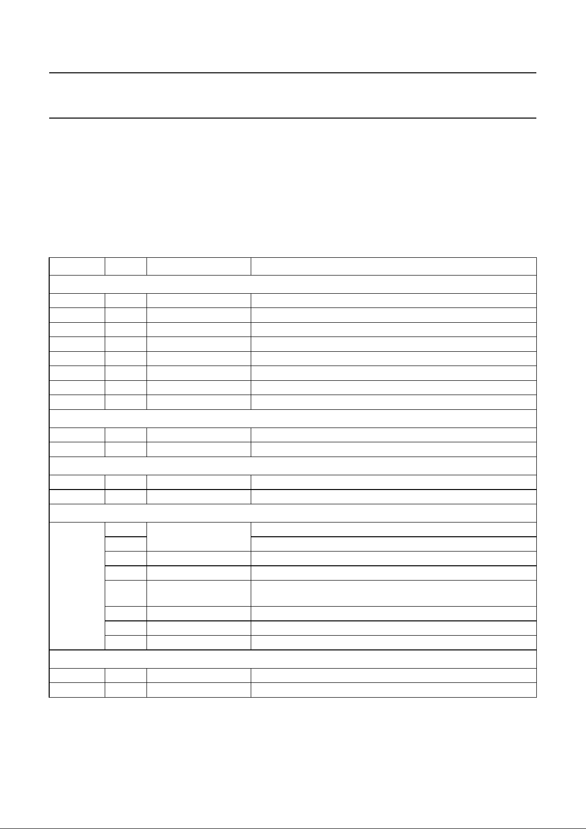
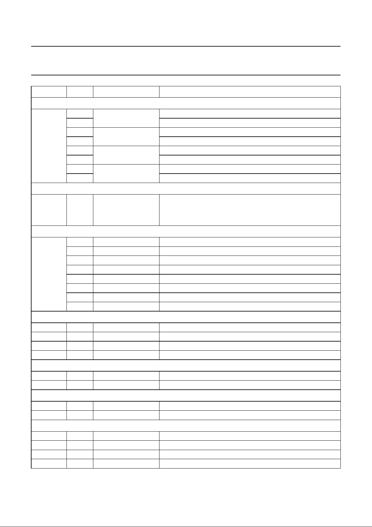
Table 1 Registers of the ECOBENDIC
REGISTER BIT NAME FUNCTION
Registers 00H to 07H (column set)
00H 0to 7 set all registers of columns 0XH and 8XH
01H 0to 7 set all registers of columns 1XH and 9XH
02H 0to 7 set all registers of columns 2XH and AXH
03H 0to 7 set all registers of columns 3XH and BXH
04H 0to 7 set all registers of columns 4XH and CXH
05H 0to 7 set all registers of columns 5XH and DXH
06H 0to 7 set all registers of columns 6XH and EXH
07H 0to 7 set all registers of columns 7XH and FXH
Registers 08H and 09H (blanking)
08H 0to 7 set blanking sets rising edge of signal BL when register data = CNT_F
09H 0to 7 reset blanking sets falling edge of signal BL when register data = CNT_F
Registers 0AH and 0BH (interrupt)
0AH 0 to 8 set CB_intAb CNT_B value when Acquisition B Interrupt (CB_intAb) is triggered
0BH 0 to 8 set CD_intDb CNT_D value when Display Interrupt (CD_intDb) is triggered
Register 0CH (YUV control)
0CH 0 phase compensation λ value for phase compensation filter, bit 0
1 λ value for phase compensation filter, bit 1
2 not used
3 Y OUT Y clipping, 0 = off, 1 = on
4 inv_UV inverts UV signals after UV processing;
0 = no inversion, 1 = inversion
5 UVbin reformatter; 1 = binary, 0 = twos complement
6 UV8bit reformatter; 1 = 8-bit quantization, 0 = 7-bit quantization
7 Sel_PixRep 1 = pixel repetition, 0 = constant colour for framing
Registers 0DH and 0EH (H2 generation)
0DH no data update start scan after addressing rising edge of H2 is set
0EH no data update start flyback after addressing falling edge of H2 is set
Page 16
1996 Oct 25 16
Philips Semiconductors Preliminary specification
Economical video processing IC
(ECOBENDIC)
SAA4970T
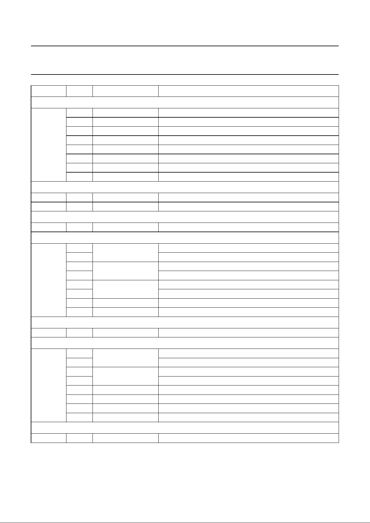
Register 0FH (internal control register)
0FH 0 not used
1 VI1_Hs output enable enables internal generation of VI1 and Hs signals (= 1)
2 MC1_select selects clock rate of MC1; 1: MC1 =
1
⁄4CK1; 0: MC1 = CK1
3 MC2_select selects clock rate of MC2; 1: MC2 =
1
⁄4CK2; 0: MC2 = CK2
4 VI2 output enable enables internal generation of VI2 (= 1)
50
60
7 CNT_D reset enable enables reset of CNT_D by VI2 (= 1)
Registers 10H and 11H (H2)
10H 0to 7 set H2 CNT_F value when rising edge of signal H2 occurs
11H 0 to 7 reset H2 CNT_F value when falling edge of signal H2 occurs
Register 12H (reset CNT_C)
12H 0to 8 reset CNT_C resets CNT_C when register data = CNT_B
Register 13H (peaking)
13H 0 Alpha α, bit 0; see Table 2
1 α, bit 1; see Table 2
2 Beta β, bit 0; see Table 3
3 β, bit 1; see Table 3
4 Coring coring value, bit 0; see Table 4
5 coring value, bit 1; see Table 4
6 not used
7 not used
Register 14H (reset CNT_D)
14H no data reset CNT_D resets CNT_D when address 14H is sent
Register 15H (DCTI)
15H 0 DCTI range K range, bit 0; see Table 5
1 K range, bit 1; see Table 5
2 DCTI gain K gain, bit 0; see Table 6
3 K gain, bit 1; see Table 6
4 hill_protect over the hill protection; 1 = on, 0 = off
5 not used
6 not used
7 not used
Register 16H (frame Y)
16H 0to 7 frame Y frame grey level = 128 + register data (128 to 383)
REGISTER BIT NAME FUNCTION
Page 17
1996 Oct 25 17
Philips Semiconductors Preliminary specification
Economical video processing IC
(ECOBENDIC)
SAA4970T
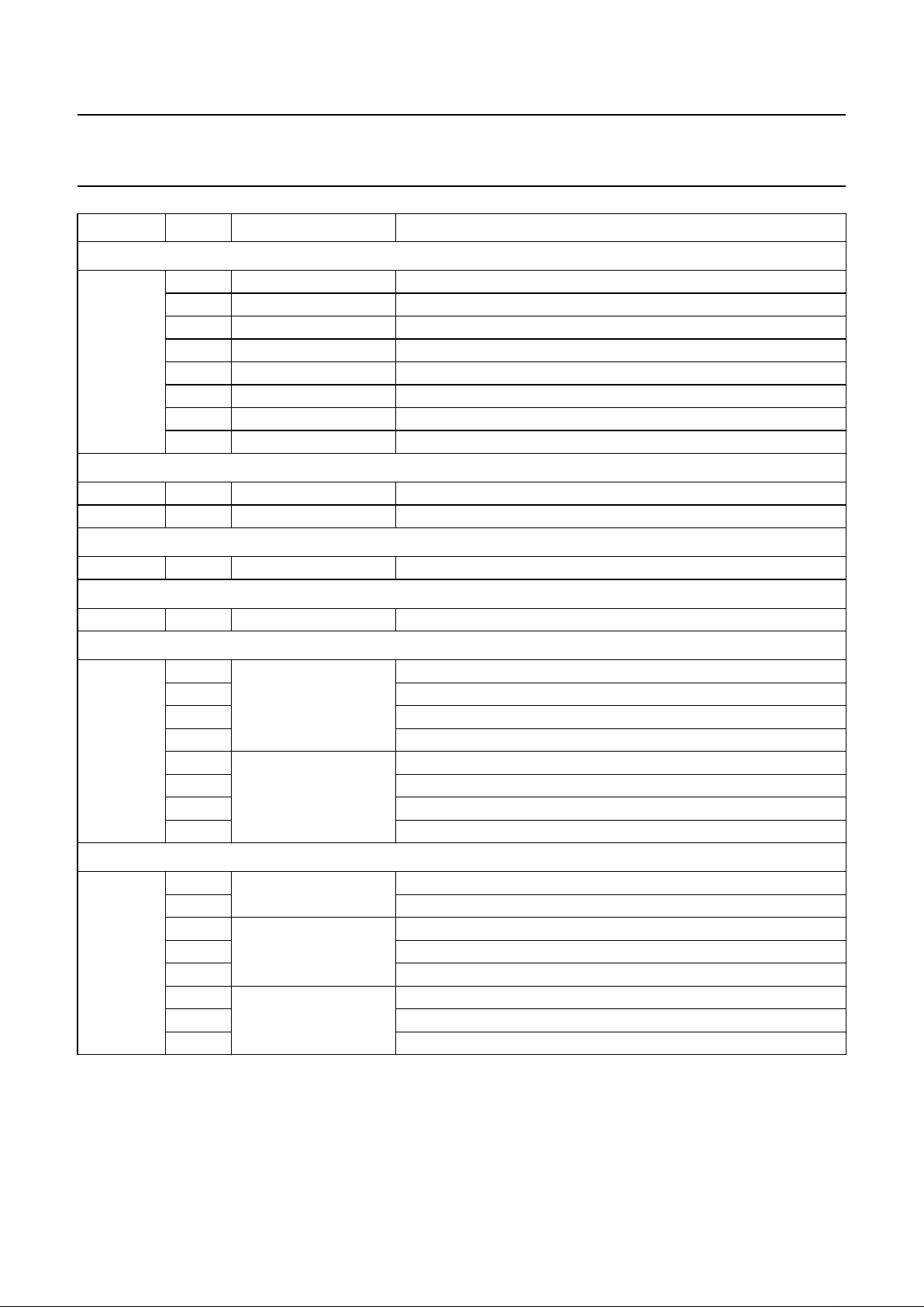
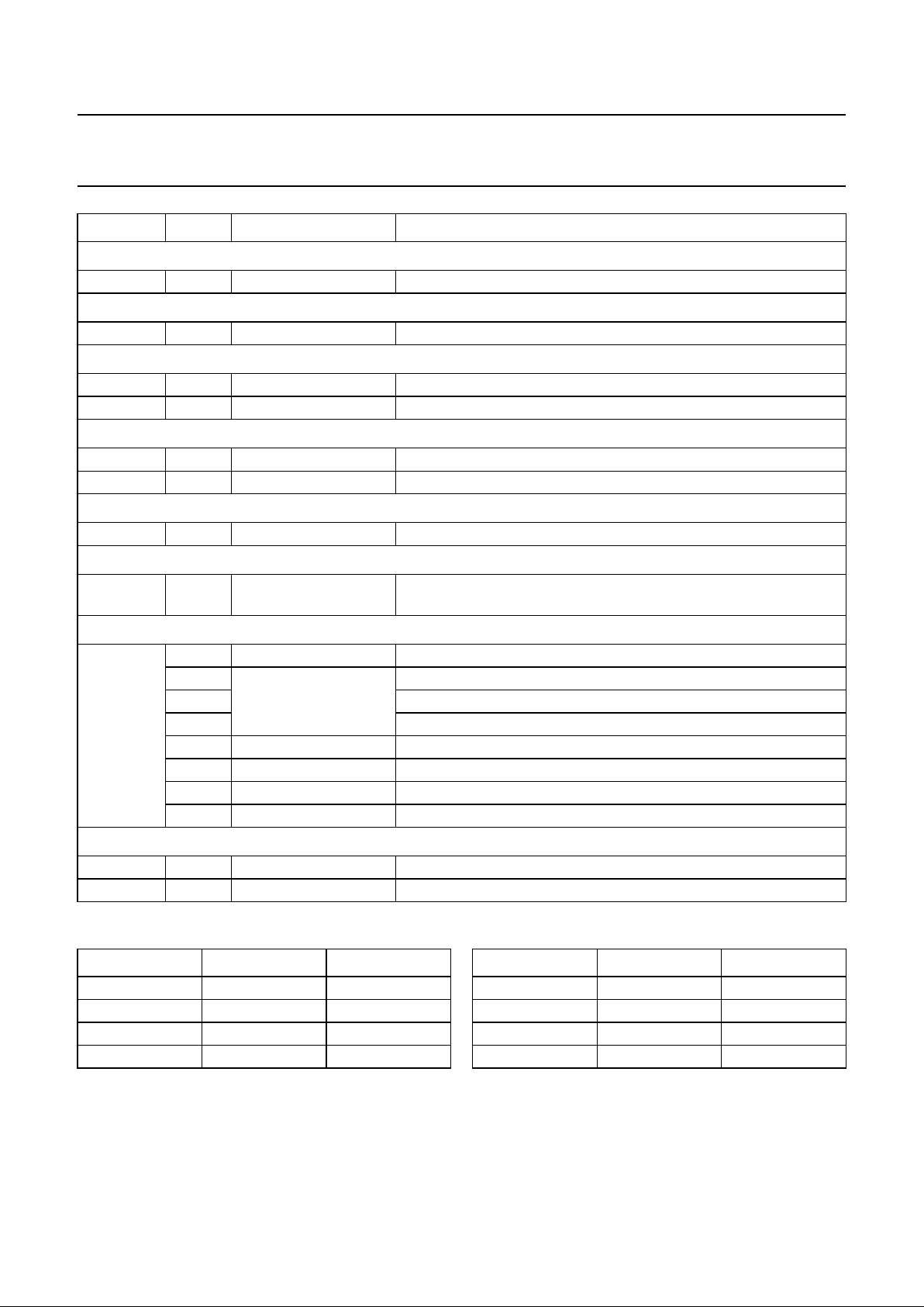
Register 17H (RE EN’s SR)
17H 0 enable set 1 enables setting of rising edge 1 of RE
1 enable set 2 enables setting of rising edge 2 of RE
2 enable reset 1 enables setting of falling edge 1 of RE
3 enable reset 2 enables setting of falling edge 2 of RE
4 not used
5 not used
6 not used
7 not used
Registers 18H and 19H (KADer)
18H 0to 7 set 3 KAD sets third rising edge of KAD signal when register data = CNT_F
19H 0to 7 reset 3 KAD sets third falling edge of KAD signal when register data = CNT_F
Register 1AH (update Len GE)
1AH 0 to 8 update Len GE sets rising edge of GE signal when register data = CNT_C
Register 1BH (reset CNT_F)
1BH 0 to 7 reset CNT_F resets CNT_F when register data = CNT_F
Register 1DH (frame UV)
1DH 0 frame U frame U level (0 to 15), bit 0
1 frame U level (0 to 15), bit 1
2 frame U level (0 to 15), bit 2
3 frame U level (0 to 15), bit 3
4 frame V frame V level (0 to 15), bit 0
5 frame V level (0 to 15), bit 1
6 frame V level (0 to 15), bit 2
7 frame V level (0 to 15), bit 3
Register 1EH (delay)
1EH 0 MC2_PROC module delay of MC2, bit 0
1 delay of MC2, bit 1
2 OUT_DELAY module delay of UV against Y signal, bit 0; see Table 8
3 delay of UV against Y signal, bit 1; see Table 8
4 delay of UV against Y signal, bit 2; see Table 8
5 IN_DELAY module delay of Y signal against UV signals, bit 0; see Table 9
6 delay of Y signal against UV signals, bit 1; see Table 9
7 delay of Y signal against UV signals, bit 2; see Table 9
REGISTER BIT NAME FUNCTION
Page 18
1996 Oct 25 18
Philips Semiconductors Preliminary specification
Economical video processing IC
(ECOBENDIC)
SAA4970T
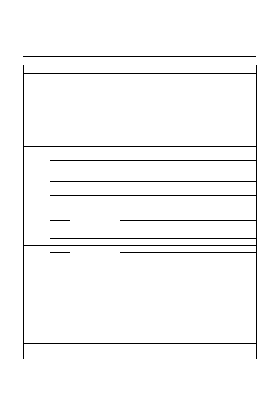
Register 1FH (BL, H2 EN’s SR)
1FH 0 enable set BL enables rising edge of BL
1 enable reset BL enables falling edge of BL
2 enable set H2 enables rising edge of H2
3 enable reset H2 enables falling edge of H2
4 not used
5 not used
6 not used
7 not used
Registers 20H and 21H (PLL)
20H 0 PLL_CORE control 1 = free-run mode: not line-locked CK1/2 generation
0 = locked mode: CK1/CK2 generation is line-locked by Hs
1 if free-run mode (else don’t care):
1 = last frequency: generates last frequency in locked mode
0 = fixed frequency: CK1/CK2 rate is determined by PLL_div
2 PLL_div, bit 0; see Table 10
3 PLL_div, bit 1; see Table 10
4 0 (test bit)
5 DIV123 control MPIP processing; specifies dividing of CK1 and R1;
CK1
PLL_CORE
=1⁄2CK2; CK1 = div × CK1
PLL_CORE
;
R1 = div × 16 kHz (RL1); bit 0; see Table 7
6 MPIP processing; specifies dividing of CK1 and R1;
CK1
PLL_CORE
=1⁄2CK2; CK1 = div × CK1
PLL_CORE
;
R1 = div × 16 kHz (RL1); bit 1; see Table 7
7 VI1 synchronized R1 is synchronized by VI1 (= 1); no synchronisation (= 0)
21H 0 n coefficient n of PI filter (C
p
=2
−(n+1)
), bit 0
1 coefficient n of PI filter (C
p
=2
−(n+1)
), bit 1
2 coefficient n of PI filter (C
p
=2
−(n+1)
), bit 2
3 m coefficient m of PI filter (C
i
=2
−(m + 2)
), bit 0
4 coefficient m of PI filter (C
i
=2
−(m + 2)
), bit 1
5 coefficient m of PI filter (C
i
=2
−(m + 2)
), bit 2
6 coefficient m of PI filter (C
i
=2
−(m + 2)
), bit 3
71
Register 22H (update HI pos)
22H 0to 7 update HI pos when register data = CNT_A then signal HI is set and CNT_B and
CNT_C are incremented
Register 23H (reset CNT_A)
23H 0to 7 reset CNT_A resets CNT_A when register data = CNT_A; generation of R1 output
signal, if en_R1_out = 1 and oe_CK1 = 0
Register 24H (reset GI_intAa)
24H 0to 7 reset GI_intAa resets Blanking-Acquisition-Interrupt
REGISTER BIT NAME FUNCTION
Page 19
1996 Oct 25 19
Philips Semiconductors Preliminary specification
Economical video processing IC
(ECOBENDIC)
SAA4970T
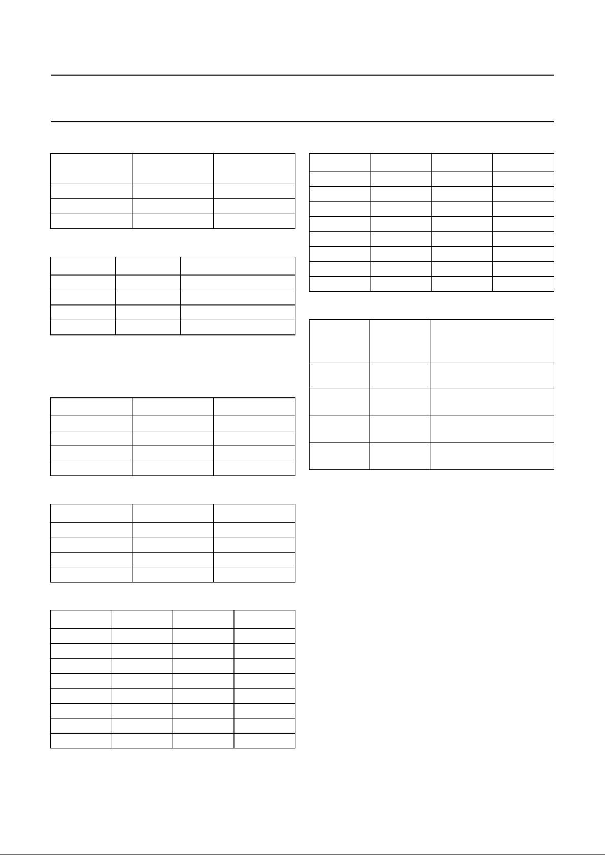
Register 25H (update G_shifts1)
25H 0 fine shift CLMP fine shift of CLMP, bit 0
1 fine shift of CLMP, bit 1
2 fine shift WE fine shift of WE, bit 0
3 fine shift of WE, bit 1
4 fine shift IE fine shift of IE, bit 0
5 fine shift of IE, bit 1
6 fine shift RE fine shift of RE, bit 0
7 fine shift of RE, bit 1
Register 26H (SAMPLE AQUI and DISPL)
26H 0to 7 SAMPLE AQUI and
DISPL
fills current value of CNT_A, CNT_B, CNT_D and CNT_F into
MUXA, MUXB, MUXE and MUXD (9th bit (MSB, bit 8) of CNT_B
into bit 4 of MUXC, 9th bit (MSB, bit 8) of CNT_D into bit 6 of
MUXC) when address 26H is sent
Register 27H (KADer EN’s SR)
27H 0 enable set 1 enables first rising edge of KAD signal
1 enable set 2 enables first falling edge of KAD signal
2 enable reset 1 enables second rising edge of KAD signal
3 enable reset 2 enables second falling edge of KAD signal
4 enable set 3 enables third rising edge of KAD signal
5 enable reset 3 enables third falling edge of KAD signal
6 not used
7 not used
Registers 28H, 29H, 2AH and 2BH (KADer)
28H 0to 7 set 1 sets first rising edge of KAD signal when register data = CNT_F
29H 0to 7 reset 1 sets first falling edge of KAD signal when register data = CNT_F
2AH 0 to 7 set 2 sets second rising edge of KAD signal when register data = CNT_F
2BH 0 to 7 reset 2 sets second falling edge of KAD signal when register data = CNT_F
Registers 2CH and 2DH (resets)
2CH no data reset CB_intAb resets interrupt CB_intAb when address 2C is sent
2DH no data reset PIP_intAc resets interrupt PIP_intAc when address 2D is sent
Registers 2EH and 2FH (window)
2EH 0 to 8 set window sets rising edge of WINDOW signal when register data = CNT_B
2FH 0 to 8 reset window sets falling edge of WINDOW signal when register data = CNT_B
Registers 30H, 31H, 32H and 33H (RE)
30H 0to 7 set 1 sets first rising edge of RE signal when register data = CNT_F
31H 0to 7 reset 1 sets first falling edge of RE signal when register data = CNT_F
32H 0to 7 set 2 sets second rising edge of RE signal when register data = CNT_F
33H 0to 7 reset 2 sets second falling edge of RE signal when register data = CNT_F
REGISTER BIT NAME FUNCTION
Page 20
1996 Oct 25 20
Philips Semiconductors Preliminary specification
Economical video processing IC
(ECOBENDIC)
SAA4970T
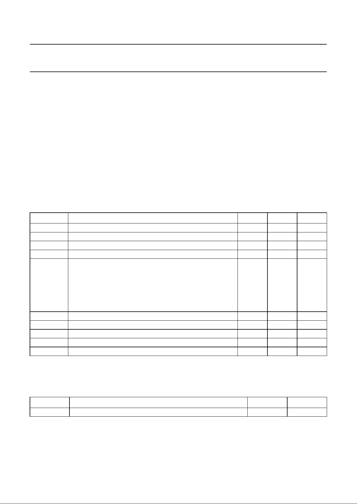
Register 34H (reset CD_intDb)
34H 0to 7 reset CD_intDb resets interrupt CD_intDb when address 34H is sent
Register 35H (set IE)
35H 0to 7 set IE sets rising edge of IE signal when register data = CNT_A
Registers 36H and 37H (win_PLL)
36H 0to 8 set win_PLL sets rising edge of win_PLL signal when register data = CNT_D
37H 0to 8 reset win_PLL sets falling edge of win_PLL signal when register data = CNT_D
Registers 38H and 39H (WE)
38H 0to 7 set WE sets rising edge of WE signal when register data = CNT_A
39H 0to 7 reset WE sets falling edge of WE signal when register data = CNT_A
Register 3AH (reset IE)
3AH 0 to 7 reset IE sets falling edge of IE signal when register data = CNT_A
Register 3BH (update VHU register)
3BH 0 to 7 update VHU register sets rising or falling edge of VI2 when register data = CNT_F and
address 0DH or 0EH is sent
Register 3DH (interrupt + R1R2_cntr)
3DH 0 0
1 Interrupt Control (IT1) enables interrupt CB_intAb
2 enables interrupt PIP_intAc
3 enables interrupt Gi_intAa
4 en_R1_out output enable R1
5 oe_CK1 output enable CK1
6 en_R2_out output enable R2
7 oe_CK2 output enable CK2
Registers 3EH and 3FH (CLMP)
3EH 0 to 7 set CLMP sets rising edge of CLMP signal when register data = CNT_A
3FH 0 to 7 reset CLMP sets falling edge of CLMP signal when register data = CNT_A
REGISTER BIT NAME FUNCTION
Table 2 α value
BIT 1 BIT 0 α VALUE
000
01
1
⁄
8
10
1
⁄
4
11
1
⁄
2
Table 3 β value
BIT 1 BIT 0 β VALUE
000
01
1
⁄
8
10
1
⁄
4
11
1
⁄
2
Page 21
1996 Oct 25 21
Philips Semiconductors Preliminary specification
Economical video processing IC
(ECOBENDIC)
SAA4970T
Table 4 Coring value
Table 5 K range
Note
1. Not useful for PAL.
Table 6 K gain
Table 7 DIV123 control
Table 8 UV delay
BIT 1 BIT 0
CORING
RANGE
0 0 +1 to −2
0 1 +3 to −4
1 0 +7 to −8
BIT 1 BIT 0 RANGE
00 ±4
01 ±6
10 ±8
11 ±12
(1)
BIT 1 BIT 0 GAIN
000
01
1
⁄
4
10
1
⁄
2
111
BIT 1 BIT 0 DIV
001
01
1
⁄
2
10
1
⁄
3
11
1
⁄
3
BIT 2 BIT 1 BIT 0 UV DELAY
000−2
001−1
0100
0111
1002
1013
1104
1115
Table 9 Y delay
Table 10 PLL_div
Read table
D
ETECTION OF ACQUISITION POSITION
MUXB/MUXA are filled with current counter values of
CNT_B/CNT_A (horizontal and vertical acquisition
position) by a positive edge of VI1 or using ‘SAMPLE AQUI
and DISPL’ register. Thus, it is possible to detect the
location of VI1 within one line by reading MUXB (CNT_B)
after VI1 has occurred.
address XXXX XX11 (03H) MUXA sampled CNT_A
value
address XXXX XX10 (02H) MUXB sampled CNT_B
value
address XXXX XX01 (01H) MUXC bit 4:
9th-bit (MSB) of sampled CNT_B.
MUXF/MUXG are filled with current counter values of
CNT_A (horizontal acquisition position) if positive/negative
edge of PIP signal occurs.
address XXXX 1000 (08H) MUXF sampled CNT_A
value by rising PIP edge
address XXXX 1100 (0CH) MUXG sampled CNT_A
value by falling PIP edge.
BIT 2 BIT 1 BIT 0 DELAY
000−3
001−2
010−1
0110
1001
1012
1103
1114
BIT 1 BIT 0
PIXEL PER LINE TO
OBTAIN DISPLAY
CLOCK CK2 FROM Hs
0 0 CK2 = 2 × 1024 × Hs
(32 MHz)
0 1 CK2 = 2 × 864 × Hs
(27 MHz)
1 0 CK2 = 2 × 768 × Hs
(24 MHz)
1 1 CK2 = 2 × 648 × Hs
(20.25 MHz)
Page 22
1996 Oct 25 22
Philips Semiconductors Preliminary specification
Economical video processing IC
(ECOBENDIC)
SAA4970T
DETECTION OF DISPLAY POSITION
MUXD/MUXE are filled with current counter values of
CNT_F/CNT_D (horizontal and vertical display position)
by a positive edge of VI2 or using the ‘SAMPLE AQUI and
DISPL’ register. Thus, it is possible to detect the location
of VI2 within one line by reading MUXD (CNT_F) after VI2
has occurred.
address XXXX 0000 (00H) MUXD sampled CNT_F
value
address XXXX 0100 (04H) MUXE sampled CNT_D
value
address XXXX XX01 (01H) MUXC bit 6:
9thbit (MSB) of sampled CNT_D.
INTERRUPT STATUS
address XXXX XX01 (01H) MUXC IT1 bit 0:
status of CB_intAb (1 = active)
address XXXX XX01 (01H) MUXC bit 1:
status of GI_intAa
address XXXX XX01 (01H) MUXC bit 2:
status of PIP_intAc
address XXXX XX01 (01H) MUXC IT2 bit 3:
status of CD_intDb.
G
ATE ENABLE (GE) STATUS
address XXXX XX01 (01H) MUXC bit 5:
status of GE (1 = enabled).
LIMITING VALUES
In accordance with the Absolute Maximum Rating System (IEC 134).
Note
1. Charge device model class B: equivalent to discharging a 200 pF capacitor through a 0 Ω series resistor.
THERMAL CHARACTERISTICS
SYMBOL PARAMETER MIN. MAX. UNIT
V
I
input voltage protection range −0.5 +7 V
V
DD
digital supply voltage (pin 42 versus pins 43 and 52) − 5.5 V
V
CC
supply voltage analog buffer (pins 6 and 10 versus pin 4) − 5.5 V
V
ref
supply voltage analog reference (pins 6 and 9 versus pin 4) − 5.25 V
I
O
output current
pins 51 and 53 versus pins 43 and 52 − 16 mA
pins 29 to 36, 11, 12, 19, 20, 25 and 26 versus pins 43 and 52 − 4mA
pins 18, 22 and 23 versus pins 43 and 52 − 8mA
pins 14 to 17 and 54 versus pins 43 and 52 − 12 mA
pins 3, 5 and 7 versus pin 4 − 20 mA
I
Osink
output sink current (pins 3, 5 and 7 versus pin 4) −−0.8 mA
P
tot
total power dissipation − 550 mW
T
stg
storage temperature −25 +125 °C
T
amb
operating ambient temperature 0 70 °C
V
es
electrostatic handling; note 1 −300 +300 V
SYMBOL PARAMETER VALUE UNIT
R
th j-a
thermal resistance from junction to ambient in free air 65 K/W
Page 23
1996 Oct 25 23
Philips Semiconductors Preliminary specification
Economical video processing IC
(ECOBENDIC)
SAA4970T
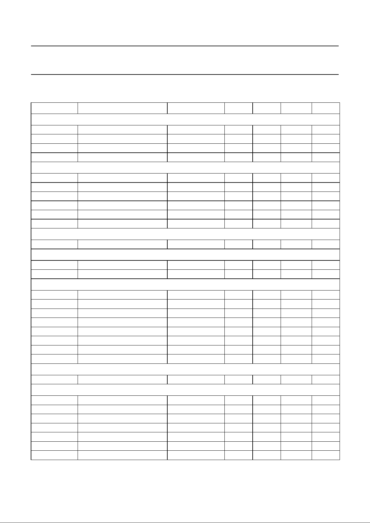
CHARACTERISTICS
T
amb
= 0 to 70 °C; VDD= 4.5 to 5.5 V; VCC= 4.75 to 5.25 V; unless otherwise specified.
SYMBOL PARAMETER CONDITIONS MIN. TYP. MAX. UNIT
Supply
V
DD
digital supply voltage 4.5 − 5.5 V
V
CC
analog supply voltage 4.75 − 5.25 V
I
DD
digital supply current −−75 mA
I
CC
analog supply current note 1 −−40 mA
Digital inputs
V
IL
LOW level input voltage −0.5 − +0.8 V
V
IH
HIGH level input voltage 2.0 − VDD+ 0.5 V
I
LI
input leakage current −−10 µA
C
IC
input capacitance (clocks) −−10 pF
C
ID
input capacitance (data) −−10 pF
C
IZ
input capacitance (I/O in high Z) −−10 pF
Reference and current inputs
I
I
input current −−0.45 mA
Digital outputs
V
OL
LOW level output voltage note 2 0 − 0.6 V
V
OH
HIGH level output voltage note 2 2.4 − V
DD
V
Timing
T
cy
CLK cycle time 27 −− ns
k
CLK
CLK duty cycle T
cyHIGH/Tcy
40 − 60 %
t
r
CLK rise time −−5ns
t
f
CLK fall time −−6ns
t
su
input data setup time −−5ns
t
h
input data hold time −−6ns
t
DOH
output data hold time note 2 3 −− ns
t
DOD
output data delay time note 2 −−25 ns
Data output loads (3-state outputs)
C
L
output load capacitance 10 − 35 pF
Characteristics of the D/A converters
RSL
Y
resolution of the Y DAC − 9 − bit
RSL
C
resolution of the U and V DAC − 8 − bit
B analog signal bandwidth (−3 dB) 20 −− MHz
α
ct
crosstalk between channels −−−42 dB
DLE differential linearity error referred to 8 MSB’s −−±0.5 LSB
ILE integral linearity error referred to 8 MSB’s −−±1 LSB
V
O
output voltage (without load) note 3 − 2 V (p-p) − V
Page 24
1996 Oct 25 24
Philips Semiconductors Preliminary specification
Economical video processing IC
(ECOBENDIC)
SAA4970T
Notes to the characteristics
1. f
CLK
= 32 MHz, f
data
= 16 MHz (rectangular full scale); without output load.
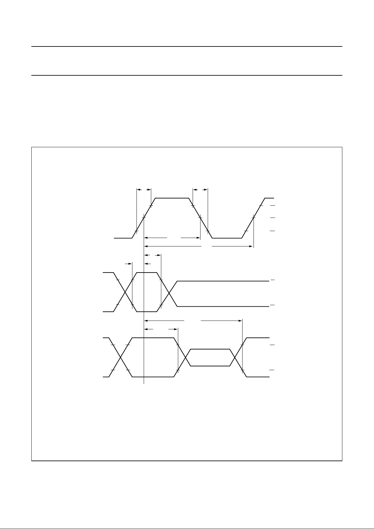
2. Timings and levels have to be measured with load circuits 1.2 kΩ connected to 3.0 V (TTL load) and CL=25pF.
3. A series resistor of 25 Ω is integrated at the outputs of the buffers. With 50 Ω in series, close to the output pins, the
nominal output voltage for 75 Ω line termination is 1 V (p-p).
Input/output timing
Fig.12 Timing diagram.
handbook, full pagewidth
MGE102
t
r
t
C27H
t
h
t
su
t
DOH
t
DOD
t
C27
t
f
2.4 V
CLOCK
CK1, CK2
INPUT
DATA
OUTPUT
DATA
1.5 V
0.6 V
2.0 V
0.8 V
2.4 V
0.6 V
Page 25

1996 Oct 25 25
Philips Semiconductors Preliminary specification
Economical video processing IC
(ECOBENDIC)
SAA4970T
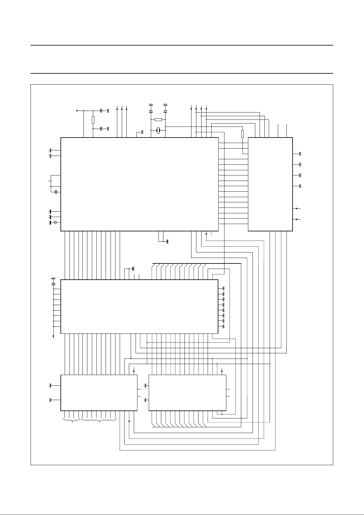
APPLICATION INFORMATION
The ECOBENDIC fits in a concept together with a triple
AD, a field memory and a microcontroller, to form a double
scan converter for YUV data.
The scan mode is AABB only. Proscan and noise
reduction are not intended with the ECOBENDIC
stand-alone. With extra processing of e.g. a Progressive
scan-Zoom and Noise reduction IC (PROZONIC
SAA4990) or Movement Estimation Line-flicker Zoom
Noise reduction IC (MELZONIC SAA4991), other scan
modes and noise reduction become possible.
All clock signals in this concept are produced by the
ECOBENDIC. The video processing is done with a
one-clock system. The read clock is frequency divided
by 2 to obtain the write clock. With the aid of a window in
which the PLL frequency is held, a phase disturbance of a
VCR will not affect the display clock stability within the
display of the active part of the video. For compression
purposes, like 4 : 3 video on a 16 : 9 display, an external
second PLL should be used. On both the acquisition and
display side, external PLLs can be applied, with 3-state
switching of the CLK signals from the ECOBENDIC.
If the field memory data can be selectively updated, then
multi picture is possible, with or without a PIP signal
blanked in the YUV input data. In the latter case the
ECOBENDIC will present a lower clock frequency to the
ADC and memory write clock. With a PIP signal blanked in
YUV, the ECOBENDIC will just manoeuvre the PIP
position into the right memory location.
The microcontroller gets the (12 MHz) clock and the
watchdog reset signals from the ECOBENDIC.
Page 26
1996 Oct 25 26
Philips Semiconductors Preliminary specification
Economical video processing IC
(ECOBENDIC)
SAA4970T
dbook, full pagewidth
MGE103
2
136
18 19
34567891011121315141617
353433323130292827262524212322
20
TMS4C2970
MEMORY
+5 V
+5 V
+5 V
87
5 12223345515674
411213446525973
888970717275767778798032062616025262728293031323536373824
23
57565554535049484744434239
2
1
19181716151413
10
987
6
40
41
636465
66
n.c.
n.c.
SAA4990H
DUVIN0
to DUVIN3
DYIN0
to DYIN7
37
10 54 1 2 6 42
24 25 26 27 28 29 30 31 32 33 34 35 36 21 20
33 14 15 18 19 36 37 38 39 40 41 42 43 2521
11235
3
2
13
11
44 23 34
10
3839404144454647484958
17
11
12
511553
16
14
SDA
SCL
8
9
735
56
55
1819232213
24
16
5
4
9
8
52
SAA4970T
87C654
MICROCONTROLLER
443
2
136
18 19
34567891011121315141617
D11
D10D9D8D7D6D5D4D3D2D1D0
D11
D10D9D8D7D6D5D4D3D2D1D0
353433323130292827262524212322
20
TMS4C2970
MEMORY
+5 V
+5 V
+5 V
+5 V
+5 V
220 Ω
6.8 kΩ
560
Ω
V
D
VOUOY
O
22 nF
22 nF
22 nF
22 nF
22 nF
HDVAH
A
150 pF
150 pF
12 MHz
Fig.13 Application diagram.
Page 27
1996 Oct 25 27
Philips Semiconductors Preliminary specification
Economical video processing IC
(ECOBENDIC)
SAA4970T
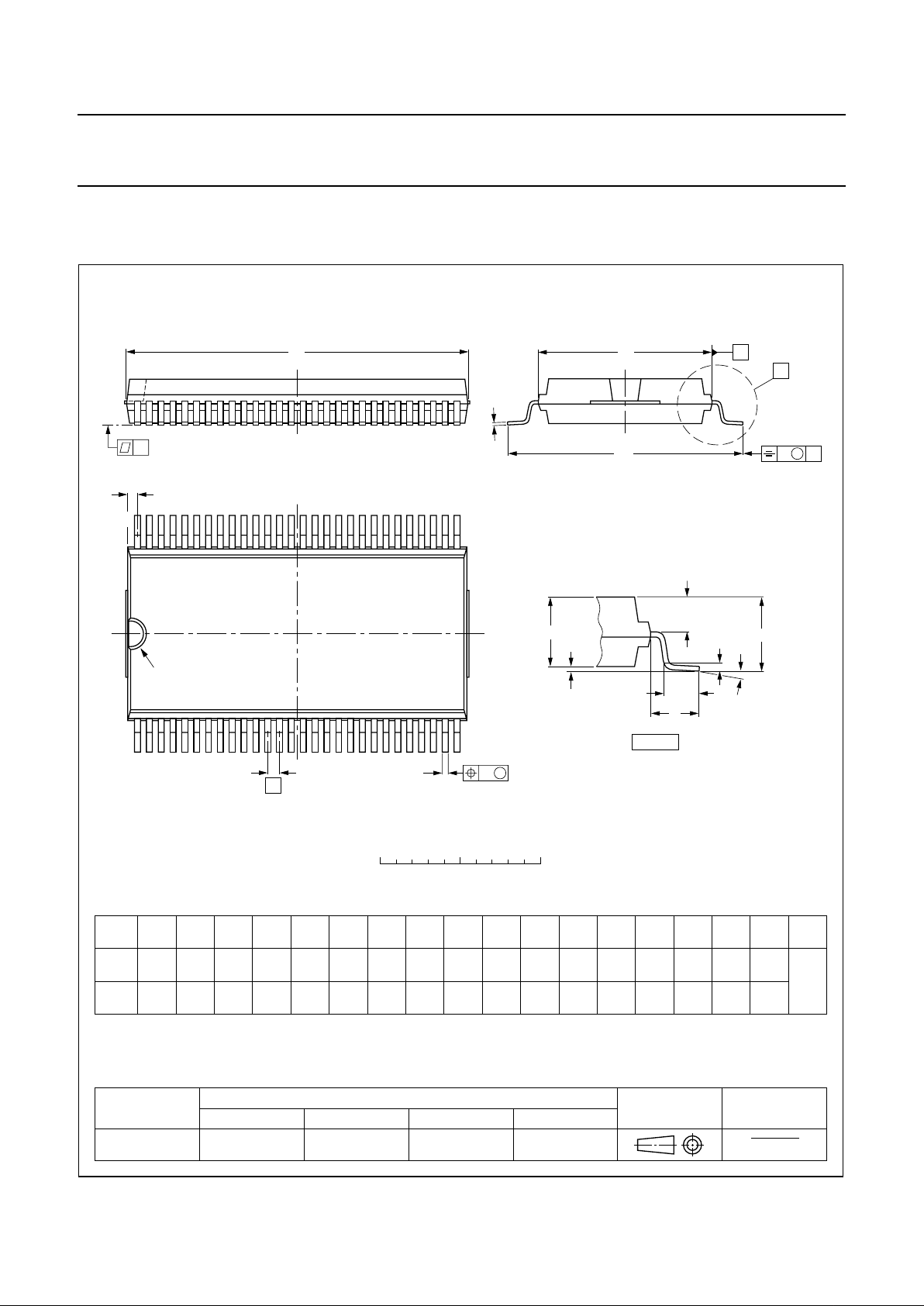
PACKAGE OUTLINE
UNIT A
1
A2A3b
p
cD
(1)E(2)
(1)
eHELLpQZywv θ
REFERENCES
OUTLINE
VERSION
EUROPEAN
PROJECTION
ISSUE DATE
IEC JEDEC EIAJ
mm
inches
0.3
0.1
3.0
2.8
0.25
0.42
0.30
0.22
0.14
21.65
21.35
11.1
11.0
0.75
15.8
15.2
1.45
1.30
0.90
0.55
7
0
o
o
0.1 0.1
DIMENSIONS (inch dimensions are derived from the original mm dimensions)
1.6
1.4
SOT190-1
92-11-17
96-04-02
w M
θ
A
A
1
A
2
b
p
D
H
E
L
p
Q
detail X
E
Z
e
c
L
v M
A
X
(A )
3
A
y
56
29
281
pin 1 index
0.012
0.004
0.12
0.11
0.017
0.012
0.0087
0.0055
0.85
0.84
0.44
0.43
0.03
2.25
0.089
0.62
0.60
0.057
0.051
0.035
0.022
0.004
0.2
0.008 0.004
0.063
0.055
0.01
0 5 10 mm
scale
VSO56: plastic very small outline package; 56 leads
SOT190-1
A
max.
3.3
0.13
Note
1. Plastic or metal protrusions of 0.3 mm maximum per side are not included.
2. Plastic interlead protrusions of 0.25 mm maximum per side are not included.
Page 28

1996 Oct 25 28
Philips Semiconductors Preliminary specification
Economical video processing IC
(ECOBENDIC)
SAA4970T
SOLDERING
Introduction
There is no soldering method that is ideal for all IC
packages. Wave soldering is often preferred when
through-hole and surface mounted components are mixed
on one printed-circuit board. However, wave soldering is
not always suitable for surface mounted ICs, or for
printed-circuits with high population densities. In these
situations reflow soldering is often used.
This text gives a very brief insight to a complex technology.
A more in-depth account of soldering ICs can be found in
our
“IC Package Databook”
(order code 9398 652 90011).
Reflow soldering
Reflow soldering techniques are suitable for all VSO
packages.
Reflow soldering requires solder paste (a suspension of
fine solder particles, flux and binding agent) to be applied
to the printed-circuit board by screen printing, stencilling or
pressure-syringe dispensing before package placement.
Several techniques exist for reflowing; for example,
thermal conduction by heated belt. Dwell times vary
between 50 and 300 seconds depending on heating
method. Typical reflow temperatures range from
215 to 250 °C.
Preheating is necessary to dry the paste and evaporate
the binding agent. Preheating duration: 45 minutes at
45 °C.
Wave soldering
Wave soldering techniques can be used for all VSO
packages if the following conditions are observed:
• A double-wave (a turbulent wave with high upward
pressure followed by a smooth laminar wave) soldering
technique should be used.
• The longitudinal axis of the package footprint must be
parallel to the solder flow.
• The package footprint must incorporate solder thieves at
the downstream end.
During placement and before soldering, the package must
be fixed with a droplet of adhesive. The adhesive can be
applied by screen printing, pin transfer or syringe
dispensing. The package can be soldered after the
adhesive is cured.
Maximum permissible solder temperature is 260 °C, and
maximum duration of package immersion in solder is
10 seconds, if cooled to less than 150 °C within
6 seconds. Typical dwell time is 4 seconds at 250 °C.
A mildly-activated flux will eliminate the need for removal
of corrosive residues in most applications.
Repairing soldered joints
Fix the component by first soldering two diagonallyopposite end leads. Use only a low voltage soldering iron
(less than 24 V) applied to the flat part of the lead. Contact
time must be limited to 10 seconds at up to 300 °C. When
using a dedicated tool, all other leads can be soldered in
one operation within 2 to 5 seconds between
270 and 320 °C.
DEFINITIONS
Data sheet status
Objective specification This data sheet contains target or goal specifications for product development.
Preliminary specification This data sheet contains preliminary data; supplementary data may be published later.
Product specification This data sheet contains final product specifications.
Limiting values
Limiting values given are in accordance with the Absolute Maximum Rating System (IEC 134). Stress above one or
more of the limiting values may cause permanent damage to the device. These are stress ratings only and operation
of the device at these or at any other conditions above those given in the Characteristics sections of the specification
is not implied. Exposure to limiting values for extended periods may affect device reliability.
Application information
Where application information is given, it is advisory and does not form part of the specification.
Page 29

1996 Oct 25 29
Philips Semiconductors Preliminary specification
Economical video processing IC
(ECOBENDIC)
SAA4970T
LIFE SUPPORT APPLICATIONS
These products are not designed for use in life support appliances, devices, or systems where malfunction of these
products can reasonably be expected to result in personal injury. Philips customers using or selling these products for
use in such applications do so at their own risk and agree to fully indemnify Philips for any damages resulting from such
improper use or sale.
Page 30

1996 Oct 25 30
Philips Semiconductors Preliminary specification
Economical video processing IC
(ECOBENDIC)
SAA4970T
NOTES
Page 31

1996 Oct 25 31
Philips Semiconductors Preliminary specification
Economical video processing IC
(ECOBENDIC)
SAA4970T
NOTES
Page 32

Internet: http://www.semiconductors.philips.com
Philips Semiconductors – a worldwide company
© Philips Electronics N.V. 1996 SCA52
All rights are reserved. Reproduction in whole or in part is prohibited without the prior written consent of the copyright owner.
The information presented in this document does not form part of any quotation or contract, is believed to be accurate and reliable and may be changed
without notice. No liability will be accepted by the publisher for any consequence of its use. Publication thereof does not convey nor imply any license
under patent- or other industrial or intellectual property rights.
Netherlands: Postbus 90050, 5600 PB EINDHOVEN, Bldg. VB,
Tel. +31 40 27 82785, Fax. +31 40 27 88399
New Zealand: 2 Wagener Place, C.P.O. Box 1041, AUCKLAND,
Tel. +64 9 849 4160, Fax. +64 9 849 7811
Norway: Box 1, Manglerud 0612, OSLO,
Tel. +47 22 74 8000, Fax. +47 22 74 8341
Philippines: Philips Semiconductors Philippines Inc.,
106 Valero St. Salcedo Village, P.O. Box 2108 MCC, MAKATI,
Metro MANILA, Tel. +63 2 816 6380, Fax. +63 2 817 3474
Poland: Ul. Lukiska 10, PL 04-123 WARSZAWA,
Tel. +48 22 612 2831, Fax. +48 22 612 2327
Portugal: see Spain
Romania: see Italy
Russia: Philips Russia, Ul. Usatcheva 35A, 119048 MOSCOW,
Tel. +7 095 247 9145, Fax. +7 095 247 9144
Singapore: Lorong 1, Toa Payoh, SINGAPORE 1231,
Tel. +65 350 2538, Fax. +65 251 6500
Slovakia: see Austria
Slovenia: see Italy
South Africa: S.A. PHILIPS Pty Ltd., 195-215 Main Road Martindale,
2092 JOHANNESBURG, P.O. Box 7430 Johannesburg 2000,
Tel. +27 11 470 5911, Fax. +27 11 470 5494
South America: Rua do Rocio 220, 5th floor, Suite 51,
04552-903 São Paulo, SÃO PAULO - SP, Brazil,
Tel. +55 11 821 2333, Fax. +55 11 829 1849
Spain: Balmes 22, 08007 BARCELONA,
Tel. +34 3 301 6312, Fax. +34 3 301 4107
Sweden: Kottbygatan 7, Akalla, S-16485 STOCKHOLM,
Tel. +46 8 632 2000, Fax. +46 8 632 2745
Switzerland: Allmendstrasse 140, CH-8027 ZÜRICH,
Tel. +41 1 488 2686, Fax. +41 1 481 7730
Taiwan: PHILIPS TAIWAN Ltd., 23-30F, 66,
Chung Hsiao West Road, Sec. 1, P.O. Box 22978,
TAIPEI 100, Tel. +886 2 382 4443, Fax. +886 2 382 4444
Thailand: PHILIPS ELECTRONICS (THAILAND) Ltd.,
209/2 Sanpavuth-Bangna Road Prakanong, BANGKOK 10260,
Tel. +66 2 745 4090, Fax. +66 2 398 0793
Turkey: Talatpasa Cad. No. 5, 80640 GÜLTEPE/ISTANBUL,
Tel. +90 212 279 2770, Fax. +90 212 282 6707
Ukraine: PHILIPS UKRAINE, 4 Patrice Lumumba str., Building B, Floor 7,
252042 KIEV, Tel. +380 44 264 2776, Fax. +380 44 268 0461
United Kingdom: Philips Semiconductors Ltd., 276 Bath Road, Hayes,
MIDDLESEX UB3 5BX, Tel. +44 181 730 5000, Fax. +44 181 754 8421
United States: 811 East Arques Avenue, SUNNYVALE, CA 94088-3409,
Tel. +1 800 234 7381
Uruguay: see South America
Vietnam: see Singapore
Yugoslavia: PHILIPS, Trg N. Pasica 5/v, 11000 BEOGRAD,
Tel. +381 11 625 344, Fax.+381 11 635 777
For all other countries apply to: Philips Semiconductors, Marketing & Sales Communications,
Building BE-p, P.O. Box 218, 5600 MD EINDHOVEN, The Netherlands, Fax. +31 40 27 24825
Argentina: see South America
Australia: 34 Waterloo Road, NORTH RYDE, NSW 2113,
Tel. +61 2 9805 4455, Fax. +61 2 9805 4466
Austria: Computerstr. 6, A-1101 WIEN, P.O. Box 213,
Tel. +43 1 60 101, Fax. +43 1 60 101 1210
Belarus: Hotel Minsk Business Center, Bld. 3, r. 1211, Volodarski Str. 6,
220050 MINSK, Tel. +375 172 200 733, Fax. +375 172 200 773
Belgium: see The Netherlands
Brazil: see South America
Bulgaria: Philips Bulgaria Ltd., Energoproject, 15th floor,
51 James Bourchier Blvd., 1407 SOFIA,
Tel. +359 2 689 211, Fax. +359 2 689 102
Canada: PHILIPS SEMICONDUCTORS/COMPONENTS,
Tel. +1 800 234 7381
China/Hong Kong: 501 Hong Kong Industrial Technology Centre,
72 Tat Chee Avenue, Kowloon Tong, HONG KONG,
Tel. +852 2319 7888, Fax. +852 2319 7700
Colombia: see South America
Czech Republic: see Austria
Denmark: Prags Boulevard 80, PB 1919, DK-2300 COPENHAGEN S,
Tel. +45 32 88 2636, Fax. +45 31 57 1949
Finland: Sinikalliontie 3, FIN-02630 ESPOO,
Tel. +358 9 615800, Fax. +358 9 61580/xxx
France: 4 Rue du Port-aux-Vins, BP317, 92156 SURESNES Cedex,
Tel. +33 1 40 99 6161, Fax. +33 1 40 99 6427
Germany: Hammerbrookstraße 69, D-20097 HAMBURG,
Tel. +49 40 23 53 60, Fax. +49 40 23 536 300
Greece: No. 15, 25th March Street, GR 17778 TAVROS/ATHENS,
Tel. +30 1 4894 339/239, Fax. +30 1 4814 240
Hungary: see Austria
India: Philips INDIA Ltd, Shivsagar Estate, A Block, Dr. Annie Besant Rd.
Worli, MUMBAI 400 018, Tel. +91 22 4938 541, Fax. +91 22 4938 722
Indonesia: see Singapore
Ireland: Newstead, Clonskeagh, DUBLIN 14,
Tel. +353 1 7640 000, Fax. +353 1 7640 200
Israel: RAPAC Electronics, 7 Kehilat Saloniki St, TEL AVIV 61180,
Tel. +972 3 645 0444, Fax. +972 3 649 1007
Italy: PHILIPS SEMICONDUCTORS, Piazza IV Novembre 3,
20124 MILANO, Tel. +39 2 6752 2531, Fax. +39 2 6752 2557
Japan: Philips Bldg 13-37, Kohnan 2-chome, Minato-ku, TOKYO 108,
Tel. +81 3 3740 5130, Fax. +81 3 3740 5077
Korea: Philips House, 260-199 Itaewon-dong, Yongsan-ku, SEOUL,
Tel. +82 2 709 1412, Fax. +82 2 709 1415
Malaysia: No. 76 Jalan Universiti, 46200 PETALING JAYA, SELANGOR,
Tel. +60 3 750 5214, Fax. +60 3 757 4880
Mexico: 5900 Gateway East, Suite 200, EL PASO, TEXAS 79905,
Tel. +9-5 800 234 7381
Middle East: see Italy
Printed in The Netherlands 537021/10/01/pp32 Date of release: 1996 Oct 25 Document order number: 9397 750 01436
 Loading...