

Page 1

INTEGRATED CIRCUITS
DATA SH EET
SAA4700
VPS dataline processor
Preliminary specification
File under Integrated Circuits, IC02
March 1991
Page 2
Philips Semiconductors Preliminary specification
VPS dataline processor SAA4700
FEATURES
• Adaptive sync slicer with buffered
composite sync output VCS
• Adaptive data slicer
• Data rate clock regenerator
• Field selection and line 16
decoding
• Startcode and biphase check
• Data valid output
• Storage of data line information in a
40 bit register bank
• I2C-bus transmission
GENERAL DESCRIPTION
The SAA4700 is a bipolar integrated
circuit designed for use in dataline
receivers and incorporates a dataline
slicer and decoder. The slicer extracts
the dataline signal from the video
signal and regenerates the data
clock. It also provides signals for the
decoder in order to decode the binary
data that is transmitted in line 16 of
every first field of the composite video
signal (video programming signal and
video recording programming by
Teletext, VPS and VPT systems).
The decoded information out of words
5 and 11 to 14 is accessed via the
built-in I
2
C-bus interface. This
information then can be used for
programming a video cassette
recorder in order to start and stop a
recording of a television program at
the correct aligned time, regardless of
a delay or extension in the
transmission time of the required
program.
QUICK REFERENCE DATA
SYMBOL PARAMETER MIN. TYP. MAX. UNIT
V
P
supply voltage (pins 15 and
4.5 5 5.5 V
16)
I
P
V
i CVBS
total supply current − 18 23 mA
CVBS input signal
sync-to-white
(peak-to-peak value) 0.5 1 1.4 V
T
amb
operating ambient
0 −+70 °C
temperature
ORDERING AND PACKAGE INFORMATION
EXTENDED TYPE
NUMBER
PINS PIN POSITION MATERIAL CODE
PACKAGE
SAA4700 18 DIL plastic SOT102
Note
1. SOT102-1; 1996 December 4.
(1)
March 1991 2
Page 3
Philips Semiconductors Preliminary specification
VPS dataline processor SAA4700
handbook, full pagewidth
4.7 nF
CVBS
470 pF
1 nF
4.7
kΩ
75 kΩ
(2%)
to V
P
4.7 nF
22
nF
2
SYNC
SEPARATOR
SAA4700
1
13
17
DATA
SLICER
REGENERATOR
PLL WITH
5 MHz VCO AND
PHASE DETECTOR
CSO
0.1
µF
5 6 11 12 7
FIELD SELECTOR
LINE 16 DECODER
line 16
data
CLOCK
VCS
14 3 4 15 16 10
(test line 16)
INPUT
CONTROLLER
TIME BASE
DAV
OUTPUT
CONTROLLER
data
4
6
REFERENCE
POWER-ON RESET
I2C-BUS
CONTROL
5
40-BIT DATA
REGISTER
40-BIT
DATA LATCH
MULTIPLEXER
VOLTAGES
8
AD = LOW
external
reset
8
SCL
9
SDA
18
n.c.
8.2 kΩ
FUNCTIONAL DESCRIPTION
Dataline 16
The information in dataline 16
consists of fifteen 8-bit words; the
total information content is shown in
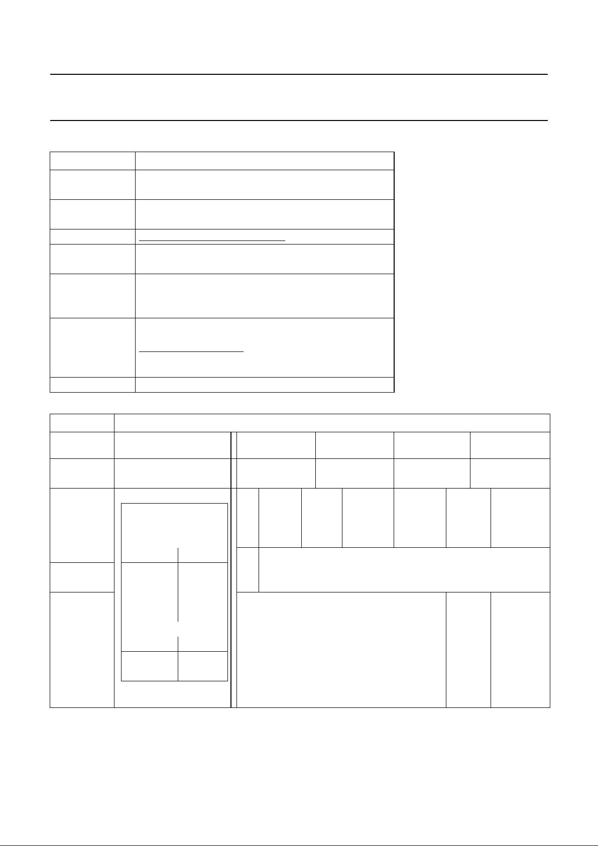
Table 1; and the organization of
transmitted bytes is shown in Table 2.
Out of the fifteen possible 8-bit words
the SAA4700 extracts words 5 and 11
to 14. The contents of these words
can be read via the built-in I
2
C-bus
interface. The circuit is fully
transparent, thus each bit is
transferred without modification with
only the sequence of words being
changed. Words 11 to 14
clock pulse
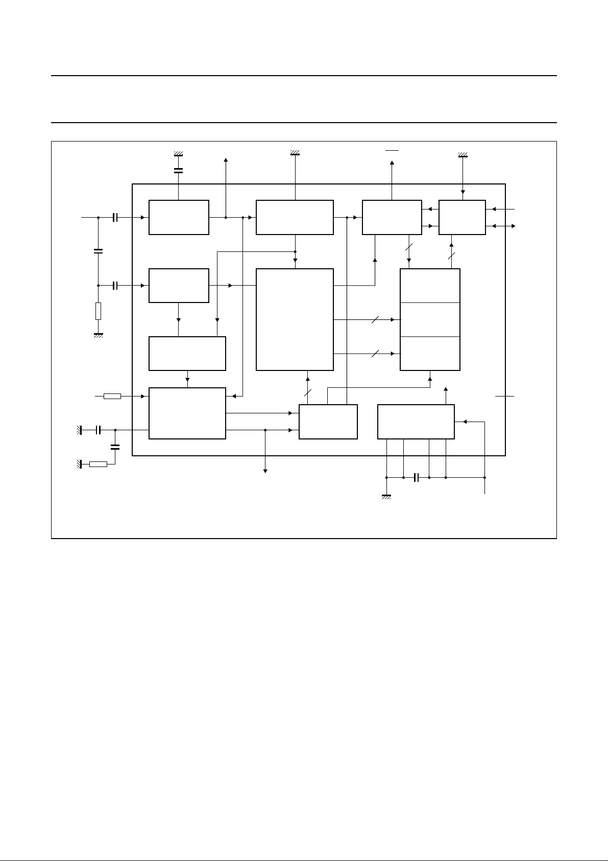
Fig.1 Block diagram and test circuit.
are transmitted first followed by
word 5.
By evaluating the sliced sync signal
the circuit can identify the beginning
of dataline 16 in the first field. The
dataline decoder stage releases the
start code detector. When a correct
start code is detected (for timing of
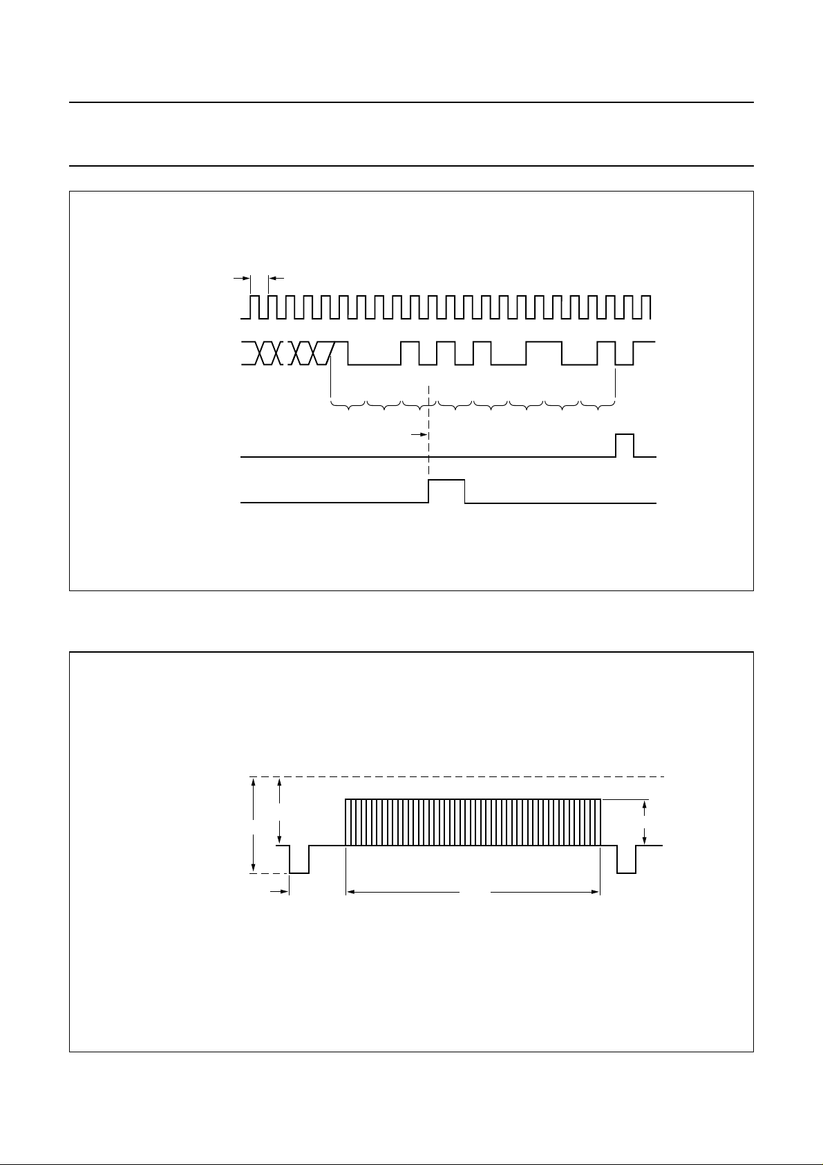
start code detection see Fig.3) words
5 and 11 to 14 are decoded, checked
for biphase errors and stored in a
register bank. If no biphase error has
occurred, the contents of the register
bank are transferred to a second
register bank by the data valid control
signal. If the system has been
addressed, this transfer will be
0.1 µF
+5 V
MEH095
V
P
delayed until the next start or stop
condition of the I2C-bus has been
received.
The last bit of correct information on
the dataline remains available until it
is read via the I2C-bus. Once the
stored information has been read it is
considered to be no longer valid and
the internal new data flag is reset.
Subsequently, if the circuit is
addressed, the only VPS data that will
be sent back is ”FFF to F”. The same
conditions apply after power-up when
no data can be read out. New data is
available after reception of another
error-free dataline 16.
March 1991 3
Page 4
Philips Semiconductors Preliminary specification
VPS dataline processor SAA4700
PINNING
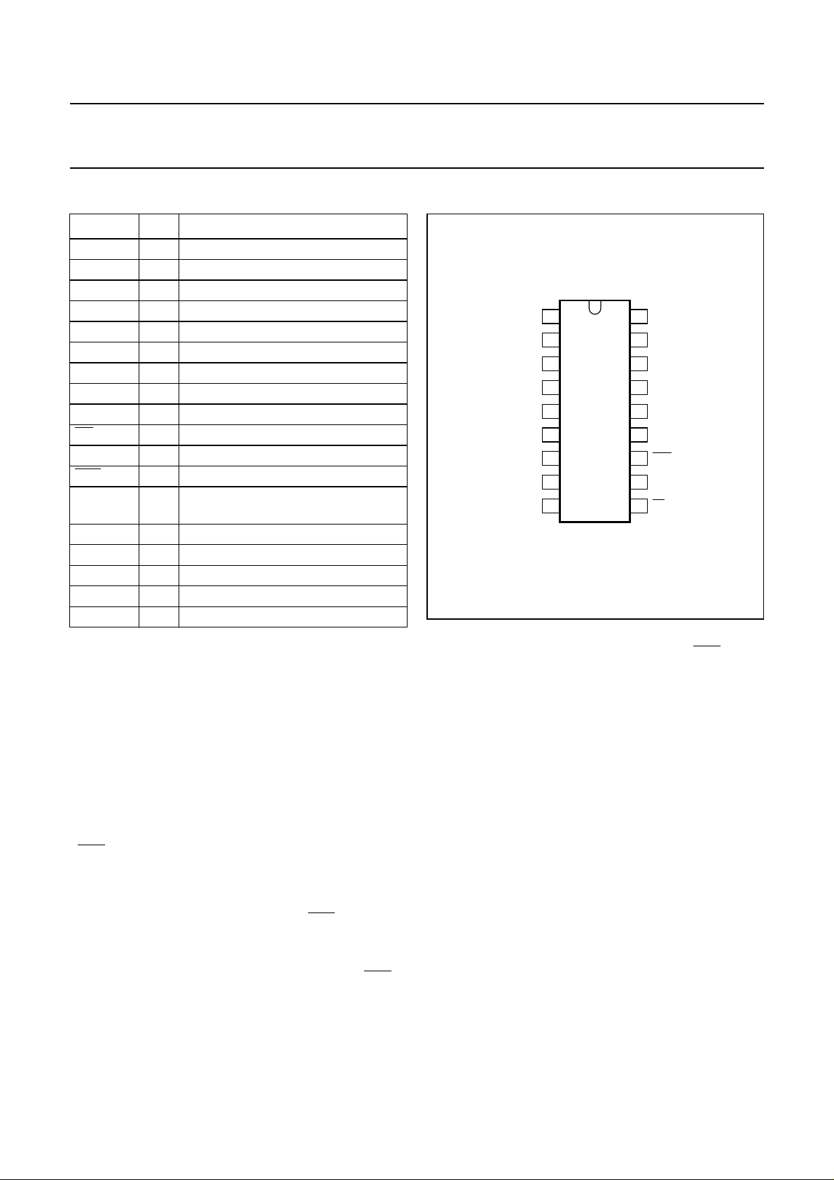
SYMBOL PIN DESCRIPTION
CVBS 1 video signal input (CVBS from TV)
SYNC 2 sync amplitude input (CVBS from TV)
GND1 3 analog ground (0 V)
GND2 4 digital ground (0 V)
C
black
5 capacitor for black level
CSO 6 composite sync output
AD 7 address set input
2
SCL 8 I
SDA 9 I
C-bus clock line
2
C-bus data line
RS 10 reset input active LOW
TP 11 test point for line 16 decoder
DAV 12 data available output active LOW
oscillator resistor for frequency
R
osc
13
adjustment
CP 14 test point clock pulse
V
P1
V
P2
C
ph
15 +5 V supply voltage (digital part)
16 +5 V supply voltage (analog part)
17 capacitor of phase detector
n.c. 18 not connected
PIN CONFIGURATION
handbook, halfpage
CVBS
SYNC
GND1
GND2
C
black
CSO
SCL
SDA
AD
1
2
3
4
5
6
7
8
9
Fig.2 Pin configuration
SAA4700
MBH796
18
n.c.
C
17
ph
V
16
P2
V
15
P1
CP
14
R
13
osc
DAV
12
TP
11
RS
10
External reset
The circuit provides an internal
power-on reset. When using this
facility pin 10 should be connected to
VP or, if external reset
(RESET = LOW) is to be used pin 10
should be prepared by connecting pin
10 via a 10 kΩ pull-up resistor to VP.
Reset forces the following:
-I2C-bus not to acknowledge
- DAV output to go HIGH (pin 12)
-I2C-bus transfer register to “FFF”
CVBS input
The CVBS signal is applied to the
sync separator (pin 2) via a
decoupling capacitor and to the data
slicer (pin 1) via an RC high-pass
filter.
To enable proper storage of the sync
value in the decoupling capacitor, the
sync generator output resistance
should not exceed 1 kΩ.
Black level
The capacitor connected to pin 5
stores the black level value for the
adaptive sync slicer.
Composite sync output (CSO)
A composite sync output signal for
customer application is provided
(pin 6).
DAV output
The data available output pin 12 is set
LOW after an error free dataline 16 is
received. DAV returnes to HIGH after
the beginning of the next first field. If
no valid data is available
DAV
remains HIGH. A short duration pulse
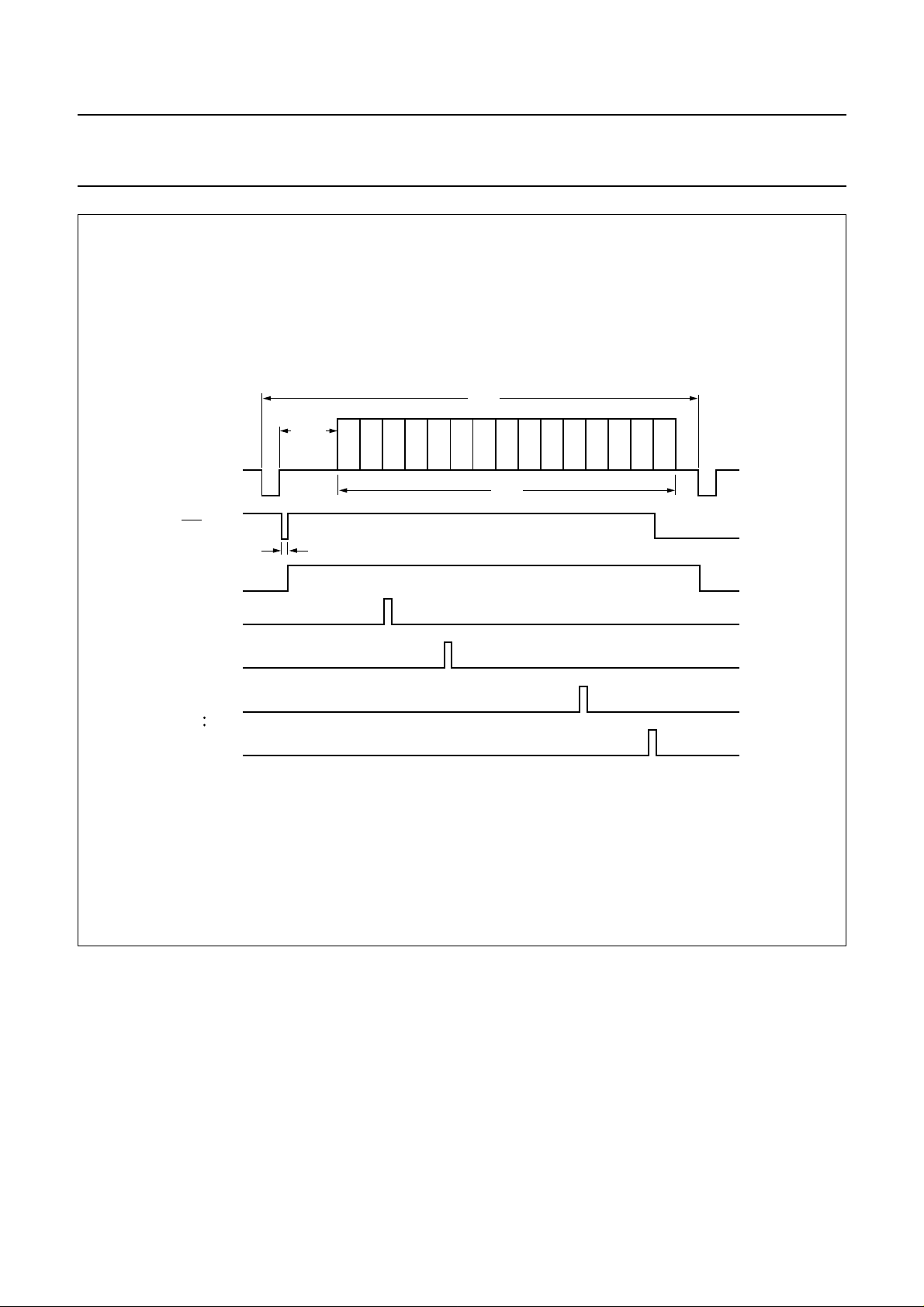
of 1 µs (Fig.5) is inserted at the
beginning of dataline 16; it will ensure
that a HIGH-to-LOW transmission
occurs which can then be used for
triggering.
5 MHz VCO and phase detector
The resistor connected between pin
13 and V
determines the current
P2
into the voltage controlled oscillator.
The RC network connected to pin 17
acts as a low-pass filter for the phase
detector.
Power supply
To prevent crosscoupling the circuit is
provided with separate ground and
supply pins for analog and digital
parts (pins 3, 4, 15 and 16).
March 1991 4
Page 5
Philips Semiconductors Preliminary specification
VPS dataline processor SAA4700
Table 1 Information per word in dataline 16
word number content
1 run in
2 start code
3 program source identification (binary coded)
4 program source identification (ASCII sequential)
5
6 program/test picture identification
7 internal information exchange
8 address assignment of signal distribution
9 address assignment of signal distribution
10 messages/commands
11
12
13
14
15 reserve
sound and VTR control information
VTR control / information
Table 2 VTR control information of dataline 16
VTR CONTROL INFORMATION
Word
number
Bit number X X X X X X X X X X X X X X X X X X X X X X X X X X X X X X X X X X X X X X X X
Label binary
System
status code
Pause
code
Interrupt
code
Word 5:
Bit1 Bit2 Status
0 1 Mono
1 0 Stereo
1 1 2-channel
Bit3 Bit4 Status
1 0 free
0 1 free
511121314
180 781516232431
AD
(1)
Day Month Hour Minute Nation
Special system code0 0 2-channel
1 X 0 0 0 0 0 1 1 1 1 1 1 1 1 1 1 1 1 1 1 1
1 X 0 0 0 0 0 1 1 1 1 1 1 1 1 0 1 1 1 1 1 1
1 X 0 0 0 0 0 1 1 1 1 1 1 1 0 1 1 1 1 1 1 1 PC...PCNC..
NC..
.NC
NC..
.NC
.NC
Progr.
source
PC...PC
PC...PC
Note
1. address range; NC = nation code; PC = program source code; X = 0 or 1 (bit)
March 1991 5
Page 6
Philips Semiconductors Preliminary specification
VPS dataline processor SAA4700
handbook, full pagewidth
data to controller
start code pulse
biphase error pulse
(ignored in word 2)
clock signal
to time base
0.2
µs
101001011011010101010
error
Fig.3 Timing diagram of start code detection.
word 3start code (word 2)run in (word 1)
1
0
MEH097
handbook, full pagewidth
white level
sync level
1 V
0.7 V
12.5 ±1.5
µs
Fig.4 Timing diagram of dataline 16; modulation depth 71.4%.
March 1991 6
48 µs
0.5 V ±5%
MEH098
Page 7
Philips Semiconductors Preliminary specification
VPS dataline processor SAA4700
handbook, full pagewidth
CVBS
DAV output
line 16
start code
pulse
word 5
latch pulse
word 11
latch pulse
word 14
latch pulse
input
12.5 µs
1 µs
word 1
word 2
word 3
word 4
word 5
64 µs
word 6
word 7
48 µs
word 8
word 9
word 10
word 11
word 12
word 13
word 14
word 15
MEH096
Fig.5 Timing diagram of the data available output and word latch pulses.
March 1991 7
Page 8
Philips Semiconductors Preliminary specification
VPS dataline processor SAA4700
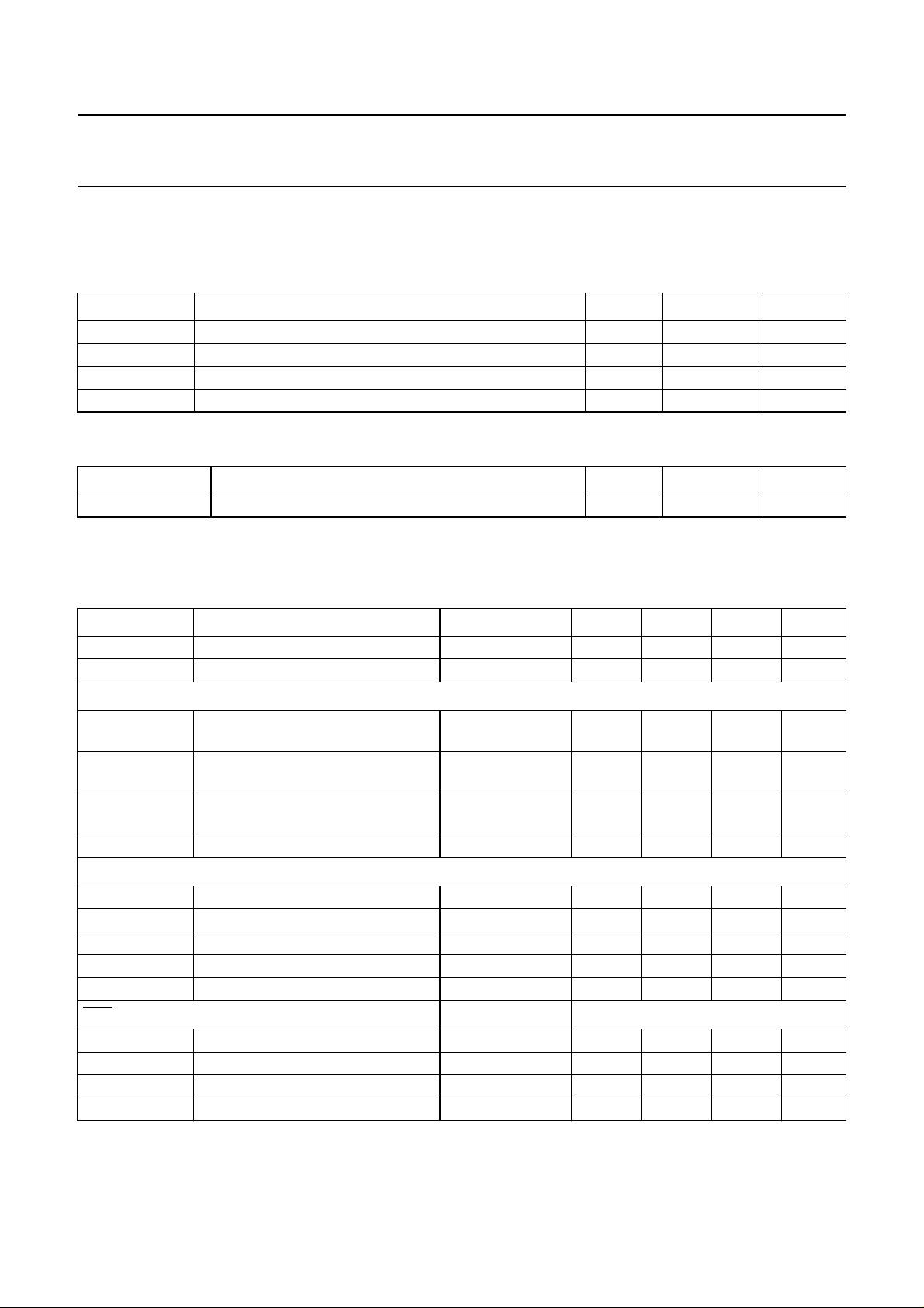
LIMITING VALUES
In accordance with the Absolute Maximum System (IEC 134).
Ground pins 3 and 4 as well as supply pins 15 and 16 tied together.
SYMBOL PARAMETER MIN. MAX. UNIT
V
P1
V
P2
T
stg
T
amb
THERMAL RESISTANCE
SYMBOL PARAMETER MIN. MAX. UNIT
R
th j-a
supply voltage (pin 15) −0.5 6.0 V
supply voltage (pin 16) −0.5 6.0 V
storage temperature range −20 125 °C
operating ambient temperature range 0 +70 °C
from junction to ambient in free air − 78 K/W
CHARACTERISTICS
= VP2 = 5 V; T
V
P1
= 25 °C; CVBS signal according to VPS and VPT standard and measurements taken in Fig.1,
amb
unless otherwise specified.
SYMBOL PARAMETER CONDITIONS MIN. TYP. MAX. UNIT
, V
V
P1
P2
I
P
supply voltages (pins 15 and 16) 4.5 5 5.5 V
total supply current I15+ I
16
− 18 23 mA
CVBS and sync inputs (pins 1 and 2)
V
i CVBS
V
i data
V
i sync
CVBS input signal
(peak-to-peak value)
data input signal
(peak-to-peak value, pin 1)
sync input signal
sync-to-white
note 1; Fig.4 0.5 1 1.4 V
line 16; Fig.4
250 500 700 mV
(peak-to-peak value, pin 2) 100 − 600 mV
R
S
source resistance −−1kΩ
Composite sync output (pin 6)
V
OL
V
OH
I
OL
I
OH
t
d
DAV output (pin 12)
V
OL
V
OH
I
OL
I
OH
output voltage LOW −−0.4 V
output voltage HIGH 2.4 −−V
output current LOW −−200 µA
output current HIGH −−−500 µA
sync separator delay time − 0.3 −µs
note 2
output voltage LOW −−0.4 V
output voltage HIGH 2.4 −−V
output current LOW −−500 µA
output current HIGH − 0.01 1 µA
March 1991 8
Page 9
Philips Semiconductors Preliminary specification
VPS dataline processor SAA4700
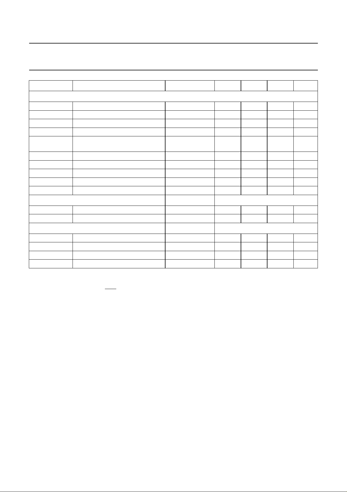
SYMBOL PARAMETER CONDITIONS MIN. TYP. MAX. UNIT
SCL and SDA (pins 8 and 9)
V
IL
V
IH
I
I
C
I
V
O ACK
t
r
t
f
t
p L
t
p H
SCL clock frequency −−100 kHz
AD set input (pin 7)
V
IL
V
IH
RESET input (pin 10)
V
IL
V
IH
I
IL
I
IH
Notes to the characteristics
1. With standard sync and data amplitude of 68% to 75% black-white.
2. If the open collector output DAV is used, a pull-up resistor to VP1 is necessary.
input voltage LOW −−1.5 V
input voltage HIGH 3 −−V
input current 0.9V
P
−−±10 µA
input capacitance −−10 pF
output voltage during acknowledge
on pin 9 IOL = 3 mA −−0.4 V
rise time −−1µs
fall time −−0.3 µs
pulse duration LOW 4.7 −−µs
pulse duration HIGH 4.0 −−µs
note 2
input voltage LOW address 23H 0 − 0.4 V
input voltage HIGH address 21H 2.4 − V
P
V
note 2
input voltage LOW reset active −−0.4 V
input voltage HIGH reset non-active 2.4 −−V
input current LOW −−−10 µA
input current HIGH − 0.01 1 µA
March 1991 9
Page 10
Philips Semiconductors Preliminary specification
VPS dataline processor SAA4700
handbook, full pagewidth
V
CVBS
P
+5 V
75 kΩ
(2%)
DAV
789
0.1
µF
CSO SCL SDA
470
pF
4.7
nF
4.7
nF
0.1 µF
SAA4700
22
nF
8.2 kΩ
n.c.
18 17 16 15 14 13 12 11 10
123456
1 nF
4.7 kΩ
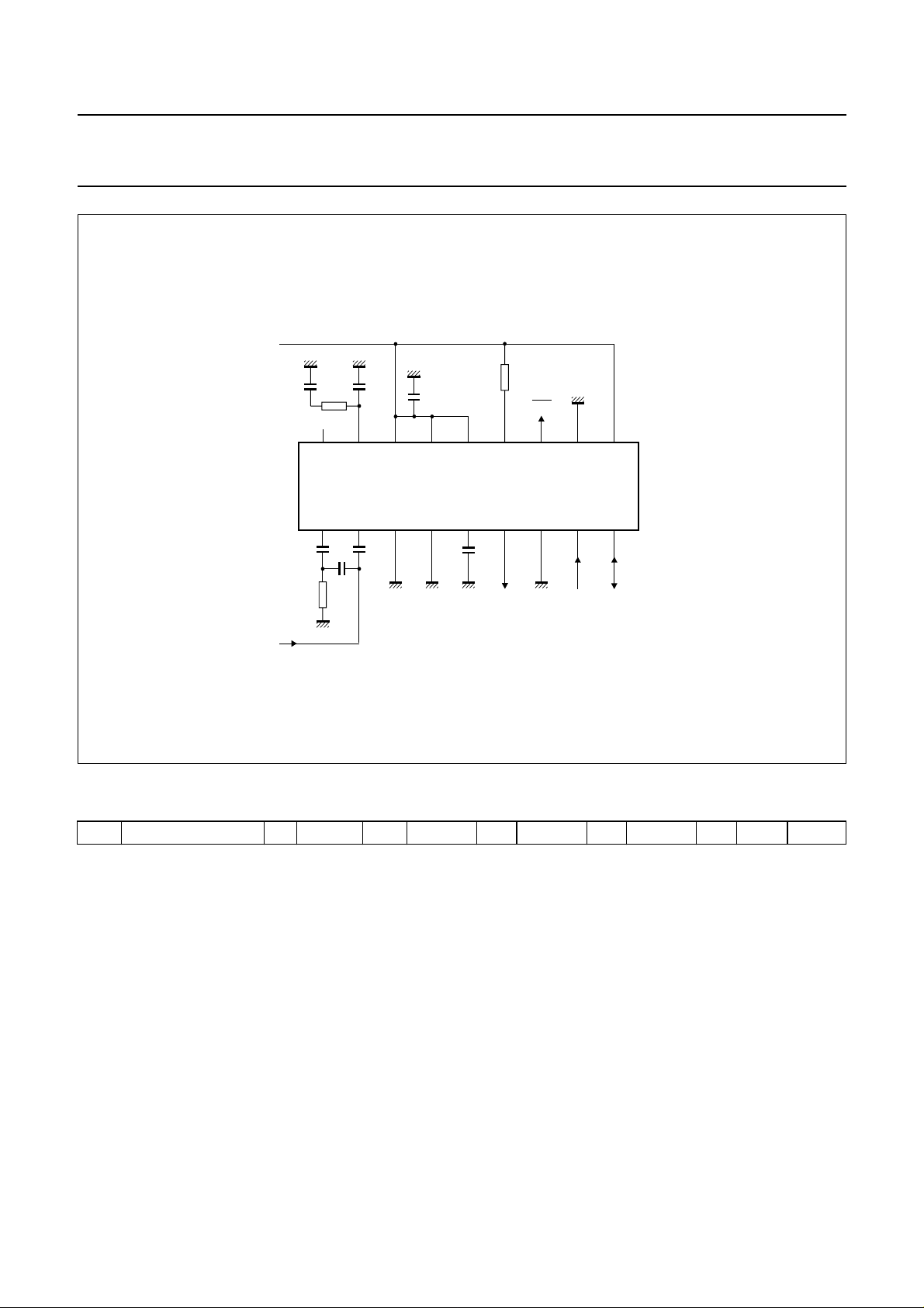
Fig.6 Application circuit.
MEH135
I2C-BUS FORMAT
S SLAVE ADDRESS A DATA A DATA A DATA A DATA A DATA P
S = start condition
SLAVE ADDRESS = 0010 0001 or 0010 0011 for set input AD = HIGH respectively LOW on pin 7
(the circuit is only a slave transmitter)
A = acknowledge, generated by the slave or the master
DATA = five data bytes, see words in Table 1
P = stop condition respectively non-acknowledge by the microcontroller
2
Remarks to I
C-bus transmission
• the MSB of each word is transmitted first
• there is no restriction on the number of words to be transmitted, but if more than five words are requested, the following
content will be “FF” continuously.
• Normally every dataline transmission has to be ended with STOP condition by non-acknowledge of the controller.
March 1991 10
Page 11
Philips Semiconductors Preliminary specification
VPS dataline processor SAA4700
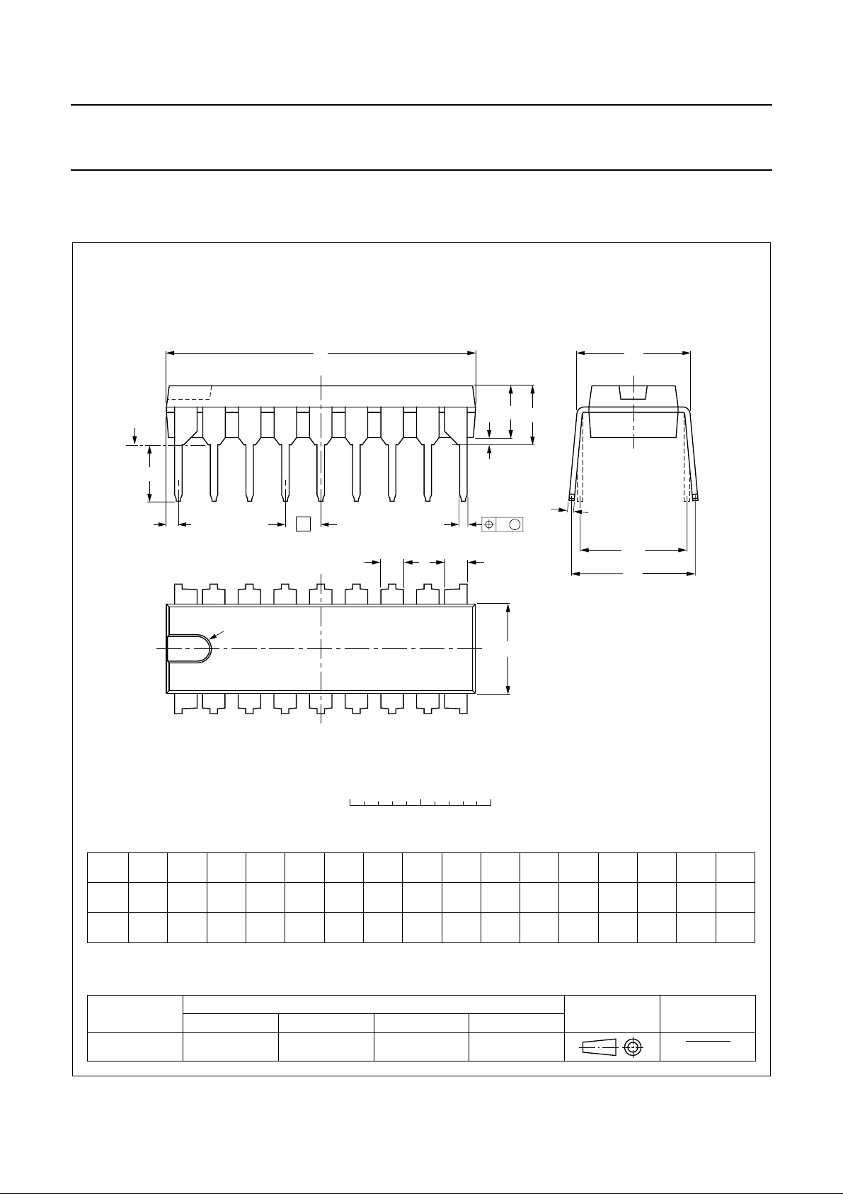
PACKAGE OUTLINE
DIP18: plastic dual in-line package; 18 leads (300 mil)
D
seating plane
L
Z
18
pin 1 index
e
b
SOT102-1
M
E
A
2
A
A
1
w M
b
1
b
2
10
E
c
(e )
1
M
H
1
0 5 10 mm
scale
DIMENSIONS (inch dimensions are derived from the original mm dimensions)
A
A
A
UNIT
max.
mm
inches
Note
1. Plastic or metal protrusions of 0.25 mm maximum per side are not included.
OUTLINE
VERSION
SOT102-1
12
min.
max.
IEC JEDEC EIAJ
b
1.40
1.14
0.055
0.044
b
1
0.53
0.38
0.021
0.015
b
cD E e M
2
0.32
1.40
0.23
1.14
0.013
0.055
0.009
0.044
REFERENCES
21.8
21.4
0.86
0.84
March 1991 11
9
(1) (1)
6.48
6.20
0.26
0.24
L
e
1
M
3.9
8.25
3.4
7.80
0.15
0.32
0.13
0.31
EUROPEAN
PROJECTION
E
0.37
0.33
H
9.5
8.3
w
max.
0.2542.54 7.62
0.854.7 0.51 3.7
0.010.10 0.30
0.0330.19 0.020 0.15
ISSUE DATE
93-10-14
95-01-23
(1)
Z
Page 12
Philips Semiconductors Preliminary specification
VPS dataline processor SAA4700
SOLDERING
Introduction
There is no soldering method that is ideal for all IC
packages. Wave soldering is often preferred when
through-hole and surface mounted components are mixed
on one printed-circuit board. However, wave soldering is
not always suitable for surface mounted ICs, or for
printed-circuits with high population densities. In these
situations reflow soldering is often used.
This text gives a very brief insight to a complex technology.
A more in-depth account of soldering ICs can be found in
“IC Package Databook”
our
(order code 9398 652 90011).
Soldering by dipping or by wave
The maximum permissible temperature of the solder is
260 °C; solder at this temperature must not be in contact
with the joint for more than 5 seconds. The total contact
time of successive solder waves must not exceed
5 seconds.
The device may be mounted up to the seating plane, but
the temperature of the plastic body must not exceed the
specified maximum storage temperature (T
stg max
). If the
printed-circuit board has been pre-heated, forced cooling
may be necessary immediately after soldering to keep the
temperature within the permissible limit.
Repairing soldered joints
Apply a low voltage soldering iron (less than 24 V) to the
lead(s) of the package, below the seating plane or not
more than 2 mm above it. If the temperature of the
soldering iron bit is less than 300 °C it may remain in
contact for up to 10 seconds. If the bit temperature is
between 300 and 400 °C, contact may be up to 5 seconds.
DEFINITIONS
Data sheet status
Objective specification This data sheet contains target or goal specifications for product development.
Preliminary specification This data sheet contains preliminary data; supplementary data may be published later.
Product specification This data sheet contains final product specifications.
Limiting values
Limiting values given are in accordance with the Absolute Maximum Rating System (IEC 134). Stress above one or
more of the limiting values may cause permanent damage to the device. These are stress ratings only and operation
of the device at these or at any other conditions above those given in the Characteristics sections of the specification
is not implied. Exposure to limiting values for extended periods may affect device reliability.
Application information
Where application information is given, it is advisory and does not form part of the specification.
LIFE SUPPORT APPLICATIONS
These products are not designed for use in life support appliances, devices, or systems where malfunction of these
products can reasonably be expected to result in personal injury. Philips customers using or selling these products for
use in such applications do so at their own risk and agree to fully indemnify Philips for any damages resulting from such
improper use or sale.
2
PURCHASE OF PHILIPS I
C COMPONENTS
Purchase of Philips I
2
C components conveys a license under the Philips’ I2C patent to use the
components in the I2C system provided the system conforms to the I2C specification defined by
Philips. This specification can be ordered using the code 9398 393 40011.
March 1991 12
 Loading...