

Page 1

INTEGRATED CIRCUITS
DATA SH EET
SAA5250
Interface for data acquisition and
control
(for multi-standard teletext
systems)
Product specification
File under Integrated Circuits, IC02
January 1987
Page 2

Philips Semiconductors Product specification
Interface for data acquisition and control
SAA5250
(for multi-standard teletext systems)
GENERAL DESCRIPTION
The SAA5250 is a CMOS Interface for Data Acquisition and Control (CIDAC) designed for use in conjunction with the
Video Input Processor (SAA5230) in a multi-standard teletext decoder. The device retrieves data from a user selected
channel (channel demultiplexer), as well as providing control signals and consecutive addressing space necessary to
drive a 2 K bytes buffer memory.
The system operates in accordance with the following transmission standards:
• French Didon Antiope specification D2 A4-2 (DIDON)
• North American Broadcast Teletext specification (NABTS)
• U.K. teletext (CEEFAX)
Features
• 7,5 MHz maximum conversion rate
• Three prefixes; DIDON, NABTS and U.K. teletext (CEEFAX)
• Mode without prefix
• Internal calculation of the validation (VAL) and colour burst blanking (CBB) signals, if programmed
• Programmable framing code and channel numbers
• Error parity calculation or not (odd parity)
• Hamming processing of the prefix byte
• Full channel or VBI reception
• Slow/fast mode (detection of page flags or not)
• Maximum/default format up to 63 bytes
• Addressing space of 2 K bytes of the static memory
• Multiplexed address/data information is compatible with Motorola or Intel microcontrollers
• CIDAC is ‘MOTEL’ compatible
PACKAGE OUTLINES
SAA5250P: 40-lead DIL; plastic (SOT129); SOT129-1; 1996 December 02.
SAA5250T: 40-lead mini-pack; plastic (VSO40); SOT158-1; 1996 December 02.
January 1987 2
Page 3
Philips Semiconductors Product specification
Interface for data acquisition and control
(for multi-standard teletext systems)
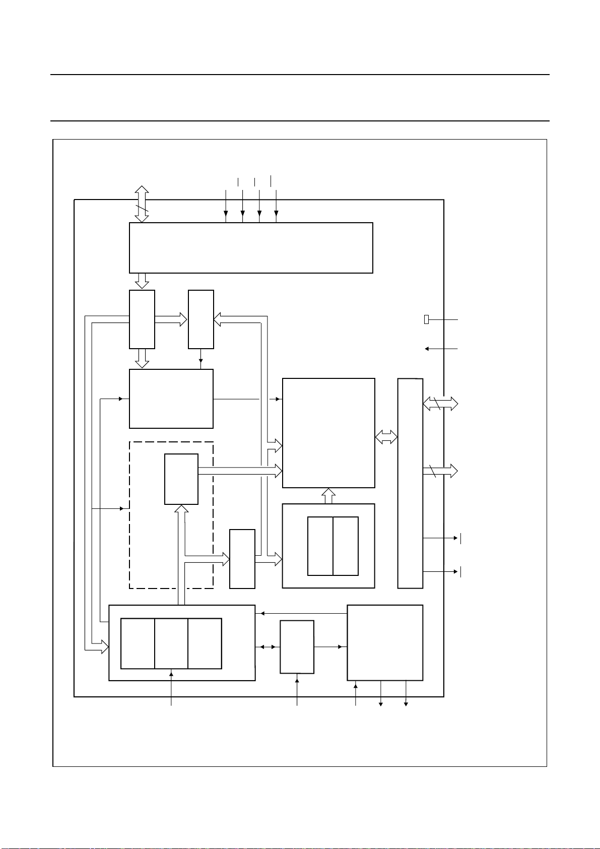
DB7toDB0
8
9-16
REGISTER
PROGRAM
17
CHANNEL
COMPARATOR
ALE
CS
RD
WR
18
21
19
INTERFACE
SAA5250
MGH075
SS
V
DD
SAA5250
, full pagewidth
PAGE DETECTION
CODE
FRAMING
DETECTION
SEQUENCE
CONTROLLER
REGISTER
SERIAL
REGISTER
PARALLEL
REGISTER
HAMMING
CORRECTOR
CONVERTER
SERIAL/PARALLEL
FORMAT
FORMAT
PROCESSOR
CLOCK
GENERATION
2 K BYTE
CONTROLLER
FIFO MEMORY
FORMAT
COUNTER
TRANSCODER
SIGNAL
VALIDATION
PROCESSING
29-22 40 20
8
1, 39-30
11
Fig.1 Block diagram.
MEMORY INTERFACE
WE A10 to A0 D7 to D0 V
78
MS
6
SD
January 1987 3
5
DCK
3
VAL IN/
SYNC
2
4
CBB
VAL OUT
Page 4
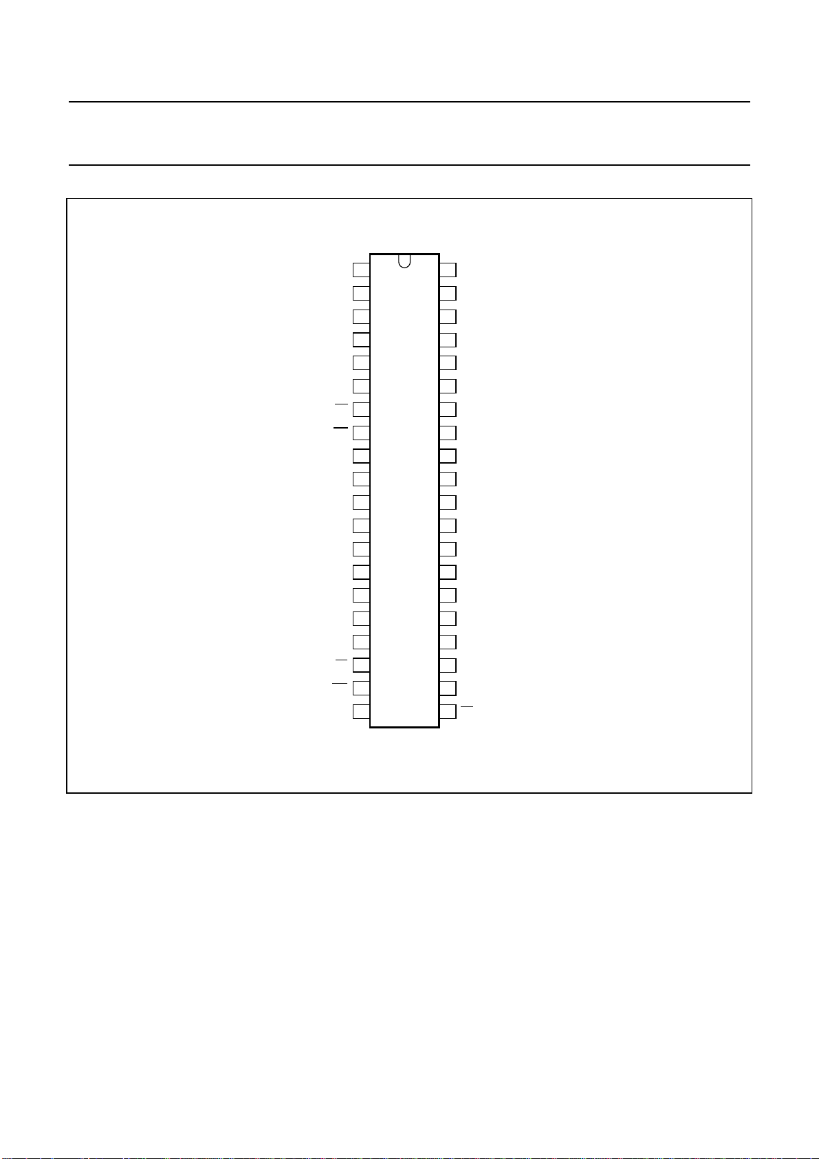
Philips Semiconductors Product specification
Interface for data acquisition and control
(for multi-standard teletext systems)
handbook, halfpage
VAL OUT
VAL IN/
A10
SYNC
CBB
DCK
SD
MS
WE
DB7
DB6
DB5
DB4
DB3
DB2
DB1
DB0
ALE
CS
WR
V
SS
1
2
3
4
5
6
7
8
9
10
11
12
13
14
15
16
17
18
19
20
SAA5250
MGH074
SAA5250
40
V
DD
39
A9
38
A8
37
A7
36
A6
35
A5
34
A4
33
A3
32
A2
31
A1
30
A0
29
D7
28
D6
27
D5
26
D4
25
D3
24
D2
23
D1
22
D0
21
RD
Fig.2 Pinning diagram.
January 1987 4
Page 5

Philips Semiconductors Product specification
Interface for data acquisition and control
SAA5250
(for multi-standard teletext systems)
PINNING FUNCTION
MNEMONIC PIN NO. FUNCTION
A10 and
A0 to A9
VAL OUT 2 Validation output signal used to control the location of the window for the framing code.
VAL IN/SYNC 3 Validation input signal (line signal) used to give or calculate a window for the framing
CBB 4 Colour burst blanking output signal used by the SAA5230 as a data slicer reset pulse
DCK 5 Data clock input, in synchronization with the serial data signal
SD 6 Serial data input, arriving from the demodulator
MS 7 Chip enable output signal for buffer memory selection
WE 8 Write command output for the buffer memory
DB7 to DB0 9 to 16 8-bit three state input/output data/address bus used to transfer commands, data and
ALE 17 Demultiplexing input signal for the CPU data bus
CE 18 Chip enable input for the SAA5250
WR 19 Write command input (when LOW)
V
SS
RD 21 Read command input (when LOW)
D0 to D7 22 to 29 8-bit three state input/output data bus used to transfer data between CIDAC and the
V
DD
1 and
30 to 39
20 ground
40 +5 V power supply
Memory address outputs used by CIDAC to address a 2 K byte buffer memory
code detection
status between the CIDAC registers and the CPU
buffer memory
January 1987 5
Page 6
Philips Semiconductors Product specification
Interface for data acquisition and control
SAA5250
(for multi-standard teletext systems)
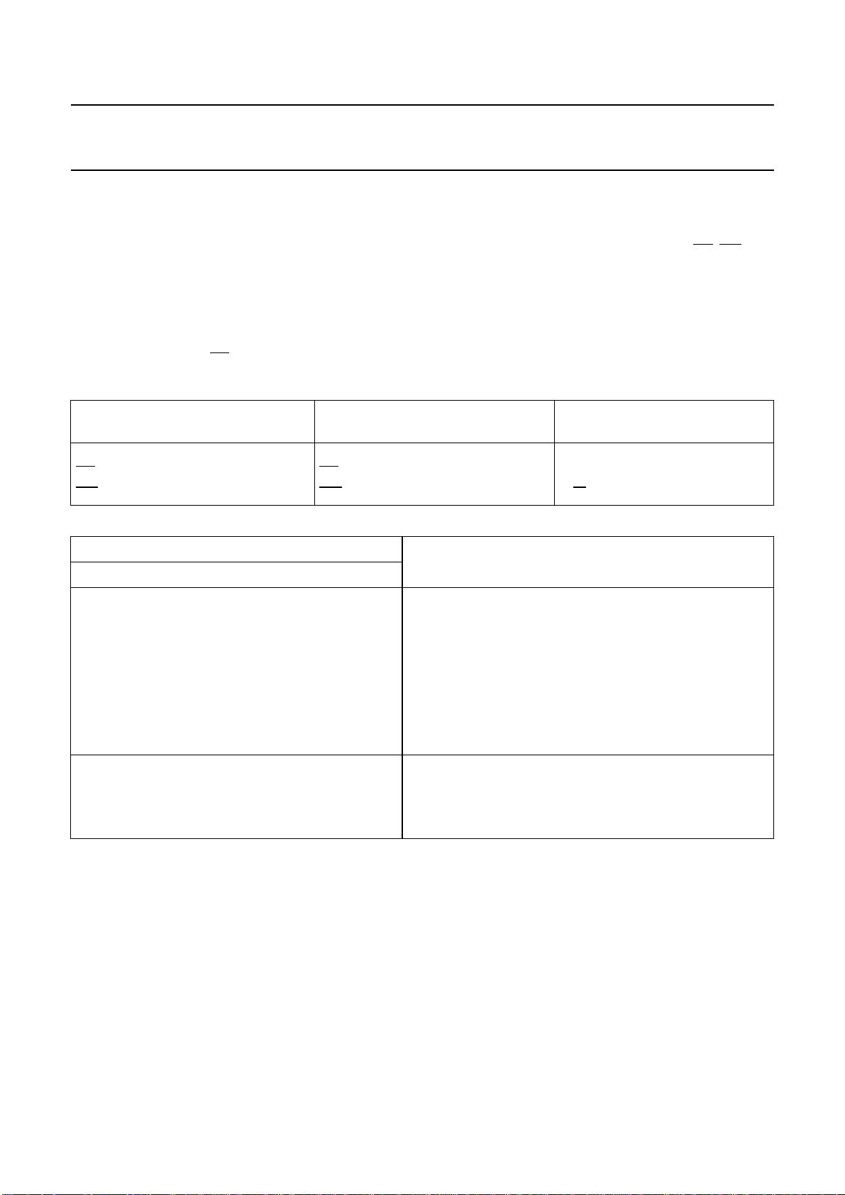
FUNCTIONAL DESCRIPTION
Microcontroller interface
The microcontroller interface communicates with the CPU via the handshake signals DB7 − DB0, ALE, CS,
microcontroller interface produces control commands as well as programming the registers to write their contents or read
incoming status/data information from the buffer memory. The details of the codes used to address the registers are
given in Table 2.
The CIDAC is ‘MOTEL’ compatible (MOTEL compatible means it is compatible with standard Motorola or Intel
microcontrollers). It automatically recognizes the microcontroller type (such as the 6801 or 8501) by using the ALE signal
to latch the state of the RD input. No external logic is required.
Table 1 Recognition signals
8049/8051
CIDAC
ALE ALE AS
RD RD DS, E, Φ 2
WR WR R/W
Table 2 CIDAC register addressing
TIMING 1
6801/6805
TIMING 2
RD,WR. The
CODES
FUNCTIONR W CS DB2 DB1 DB0
100000write register R0
100001write register R1
100010write register R2
100011write register R3
100100write register R4
100101write register R5
100110write command register R6 (initialization command)
100111write register R7
010000read status
010001read data register
010010test (not used)
010011test (not used)
January 1987 6
Page 7
Philips Semiconductors Product specification
Interface for data acquisition and control
(for multi-standard teletext systems)
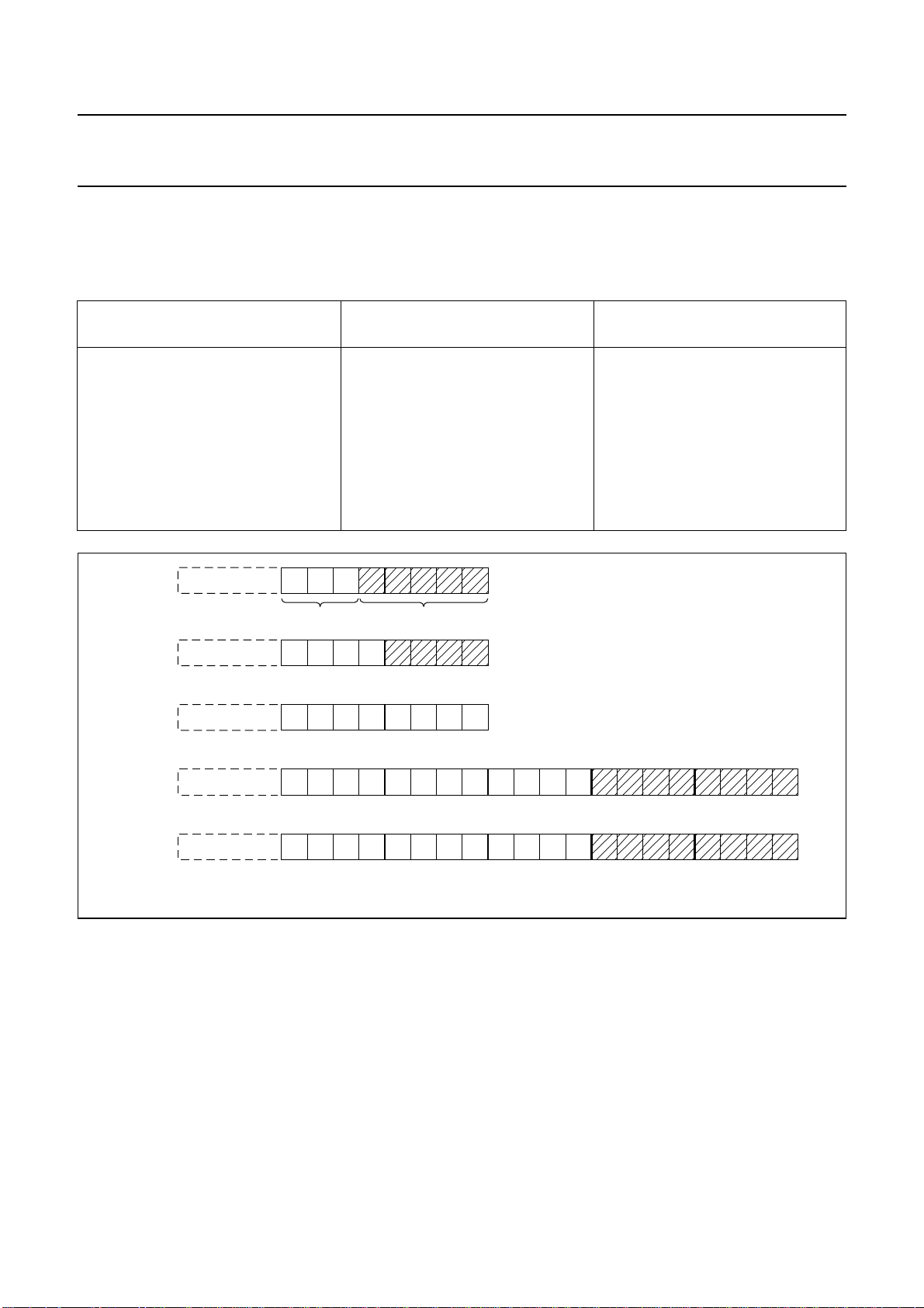
Register organization
R0 register
Table 3 R0 Register contents
R04
SLOW/FAST MODE
0 = slow mode 0 = no parity control 000 = DIDON long
1 = fast mode 1 = odd parity 001 = DIDON medium
handbook, full pagewidth
FCCEEFAX
R03
PARITY
SAA5250
R02 TO R00
USED PREFIXES
010 = DIDON short
011 = not used
100 = U.K. teletext
101 = NABTS
110 = without prefix
111 = without prefix
magazine and row address group
MRAG
format
A2
A2
A2
A3
A3
CI
CI
format
PS
MGH077
DIDON
short
DIDON
medium
DIDON
long
NABTS
A
FC
A1
FC
A1
FC
A1
FC
Fig.3 Five prefixes.
All of the bytes (see Fig.3) are Hamming protected. The hatched bytes are always stored in the memory in order to be
processed by the CPU (see section ‘Prefix processing’). In the mode without prefix all of the bytes which follow the
framing code are stored in the memory until the end of the data packet, the format is then determined by the contents of
the R3 register.
If R03 = 0; no parity control is carried out and the 8-bits of the incoming data bytes are stored in the fifo memory.
If R03 = 1; the 8th bit of the bytes following the prefix (data bytes) represents the result of the odd parity control.
If R04 = 0; the device operates in the slow mode. The CIDAC retrieves data from the user selected magazine (see
section ‘R1 and R2’) and without searching for a start to a page stores the data into the FIFO memory.
January 1987 7
Page 8

Philips Semiconductors Product specification
Interface for data acquisition and control
SAA5250
(for multi-standard teletext systems)
If R04 = 1; the device operates in the fast mode. Prior to writing into the FIFO memory, the CIDAC searches for a start
to a page which is variable due to the different prefixes:
• DIDON (long, medium and short): using the redundant bytes, SOH RS, X RS and SOH X (where X is a bit affected by
a parity error)
• NABTS, the least significant bit of the PS byte is set to 1
• U.K. teletext, ROW = 0
R1 register
Table 4 R1 Register contents
R17
VAL IN/SYNC
1 = VAL 000 = list 1 first digit hexadecimal value
0 = SYNC 001 = list 2
Note
1. X = don’t care
R16 TO R14
FORMAT TABLE
010 = list 3
011 = list 4
1XX = maximum/default value used (R3)
(1)
R13 TO R10
CHANNEL NUMBERS (FIRST DIGIT)
If VAL IN/SYNC = 1; the line signal immediately produces a validation signal for the framing code detection.
If VAL OUT = 0; the line signal is used as a starting signal for an internally processed validation signal (see Fig.15). The
framing code window width is fixed at 13 clock periods and the delay is determined by the contents of the R5 register
(R56 to R50).
At any moment the user is able to ensure that the framing code window is correctly located. This is accomplished by the
VAL OUT pin reflecting the internal validation signal. A CBB signal with programmable width (see section ‘R7 register’)
can also be generated, this is used as a data slicer reset pulse by the SAA5230. The line signal is used as the starting
point of the internal CBB signal width fixed by the contents of the R7 register.
If R16 = 0; then bits R15 and R14 provide the format table number using DIDON long and short prefixes (see Table 6).
If R16 = 1; then the format is determined by the contents of the R3 register.
The bits R13 to R10 represent the first channel number to be checked in the prefix. In U.K. teletext mode only 3 bits are
required, so R13 = X.
January 1987 8
Page 9
Philips Semiconductors Product specification
Interface for data acquisition and control
(for multi-standard teletext systems)
Table 5 Format table
FORMAT BYTE
B8, B6, B4 AND B2
0000 0 0 0 0
0001 1 1 1 1
0010 2 2 2 2
0011 3 3 3 3
0100 4 5 6 7
0101 8 9 10 11
0110 12 13 14 15
0111 16 17 18 19
1000 20 21 22 23
1001 24 25 26 27
1010 28 29 30 31
1011 3233 3435
1100 36 37 38 39
1101 40 41 42 43
1110 44 45 46 47
1111 48 49 50 51
(1)
LIST 1 LIST 2 LIST 3 LIST 4
SAA5250
Note
1. B8 = MSB and B2 = LSB.
R2 register
Table 6 R2 Register contents
R27 TO R24 R23 TO R20
channel number, third digit channel number, second digit
(hexadecimal value, third digit) (hexadecimal value, second digit
Note
1. R27 and R23 = MSB and R24 and R20 = LSB
The R2 register provides the other two parts of the channel number (depending on the prefix) that require checking.
January 1987 9
Page 10
Philips Semiconductors Product specification
Interface for data acquisition and control
SAA5250
(for multi-standard teletext systems)
R3 register
Table 7 R3 register contents
R35 TO R30
6-BIT FORMAT MAXIMUM/DEFAULT VALUE
000000 = 0
000001 = 1
−
−
−
111111 = 63
This 6-bit byte gives:
• In the DIDON long and short mode, a maximum format in case of corrupted transmission (multiple errors on the
Hamming corrector)
• A possible 63-bit format for all types of prefix
R4 register
Table 8 R4 register contents
R47 TO R40
8-bit register used for storing the framing code value which will be compared with the third byte of each data
line
R5 register
Table 9 R5 register contents
R57
NEGATIVE/POSITIVE
0 = negative edge for sync signal 7-bit sync delay, giving a maximum
1 = positive edge for sync signal delay of (2
Note
1. F = data clock acquisition frequency (DCK).
Using R57 it is possible to start the internal synchronization delay (t
R6 write command register
This is a fictitious register. Only the address code (see Table 2) is required to reset the CIDAC. See Table 11 for the
status of the FIFO memory on receipt of this command.
R7 register
Table 10 R7 register contents
R56 TO R50
SYNCHRONIZATION DELAY
7
− 1) × 106µs/F (Hz)
) on the positive or negative edge.
DVAL
R75 TO R70
6-bit register used to give a maximum colour burst blanking signal of: (26− 1) × 106µs/F (Hz)
Note
1. F = data clock acquisition frequency.
January 1987 10
Page 11

Philips Semiconductors Product specification
Interface for data acquisition and control
SAA5250
(for multi-standard teletext systems)
Fifo status register (
Table 11 Fifo register contents
DB2 TO DB0
DB2 = 1
memory empty
Once the relevant prefix and the right working modes have been given by the corresponding registers, a write command
to the R6 register enables the CIDAC to accept and process serial data.
Channel comparator
This is a four bit comparator which compares the three user hexadecimal defined values in R1 and R2 to corresponding
bytes of the prefix coming from the Hamming corrector. If the three bytes match, the internal process of the prefix
continues. If they do not match the CIDAC returns to a wait state until the next broadcast data package is received.
FIFO memory controller
The FIFO memory contains all the necessary functions required for the control of the 11-bit address memory (2 K byte).
The functions contained in the FIFO memory are as follows:
• write address register (11-bits)
• read address register (11-bits)
• memory pointer (11-bits)
• address multiplexer (11-bits)
• write data register (8-bits)
• read data register (8-bits)
• data multiplexer
• control logic
read R0 register)
DB1 = 1, data not present in the
read data register
DB0 = 0
memory not full
The FIFO memory provides the memory interface with the following:
• 11-bit address bus (A10 to A0)
• 8-bit data bus (D7 to D0)
• two control signals, memory select (MS) and write enable (WE)
January 1987 11
Page 12

Philips Semiconductors Product specification
Interface for data acquisition and control
SAA5250
(for multi-standard teletext systems)
Operation
The CIDAC uses the same clock signal for data acquisition and internal processing, this allows the CIDAC to have a write
and a read cycle during each character period (see Fig.13). The first half of the character period is a write cycle and the
second half is a read cycle. Consequently, for an 8 MHz bit rate the maximum memory cycle time is 500 ns.
When the first data byte is written into the FIFO memory, thus transferred into the read register, the FIFO memory enters
the status shown in Table 12.
Table 12 FIFO status
DB2 TO DB0
DB2 = 1
memory empty
When the FIFO memory is full two events occur:
• the write address register points to the next address after the last written address
• when new data is to be written, the memory select signal output ceases
Memory interface
DB1 = 0
data available
DB0 = 0
memory not full
The memory interface contains all the buffers for the memory signals mentioned in the section ‘FIFO memory controller’.
Page detection
This part of the CIDAC contains a parallel register with logic which detects (only in fast mode) a start of a page or data
group (see section ‘R0 register’).
Hamming correction (see Tables 13 and 14) The Hamming correction provides (see section ‘Prefix processing’):
• hexadecimal value of the Hamming code
• accept/reject code signal
• parity information
January 1987 12
Page 13

Philips Semiconductors Product specification
Interface for data acquisition and control
(for multi-standard teletext systems)
Table 13 Hamming correction (coding)
HEXADECIMAL
NOTATION
0 00010101
1 00000010
2 01001001
3 01011110
4 01100100
5 01110011
6 00111000
7 00101111
8 11010000
9 11000111
A 10001100
B 10011011
C 10100001
D 10110110
E 11111101
F 11101010
B8 B7 B6 B5 B4 B3 B2 B1
SAA5250
Note
1. B7 = B8 ⊕ B6 ⊕ B4
B5 = B6 ⊕ B4 ⊕ B2
B3 = B4 ⊕ B2 ⊕ B8
B1 = B2 ⊕ B8 ⊕ B6
⊕ = exclusive OR gate function
B8, B6, B4 and B2 = data bits
B7, B5, B3 and B1 = redundancy bits
January 1987 13
Page 14

Philips Semiconductors Product specification
Interface for data acquisition and control
(for multi-standard teletext systems)
Table 14 Hamming correction (decoding)
ABCDINTERPRETATION INFORMATION
1111no error accepted
0010error on B8 corrected
1110error on B7 accepted
0100error on B6 corrected
1100error on B5 accepted
1000error on B4 corrected
1010error on B3 accepted
0000error on B2 corrected
0110error on B1 accepted
A.B.C = 0 1 multiple errors rejected
Note
1. A = B8 ⊕ B6 ⊕ B2 ⊕ B1
B = B8 ⊕ B4 ⊕ B3 ⊕ B2
C = B6 ⊕ B5 ⊕ B4 ⊕ B2
D = B8 ⊕ B7 ⊕ B6 ⊕ B5 ⊕ B4 ⊕ B3 ⊕ B2 ⊕ B1
⊕ = exclusive OR gate function
SAA5250
Format processing
The format processing consist of two parts:
part 1
A format transcoder produces a 6-bit code (up to 63) and uses the following as inputs:
• DIDON long and short prefixes;
hamming corrected code (4-bits)
accept/reject code condition
table number (see section ‘R1 register’, bits R15 and R14)
• Other prefixes (R16 = 1)
• 6-bit maximum/default format (see section ‘R3 register’)
part 2
A format counter operating at the character clock frequency which receives the 6-bit code from the format transcoder and
is used to check the data packet length following the prefix.
Serial/parallel converter
The serial/parallel converter consists of three parts:
• An 8-bit shift register which receives the SD input and operates at the bit frequency (DCK).
• An 8-bit parallel register used for storage.
• A framing code detection circuit. This logic circuit compares the 8-bits of the R4 register with that of the serial register.
If seven bits out of eight match (in coincidence with a validation window), it produces a start signal for a new teletext
data line to the sequence controller.
January 1987 14
Page 15

Philips Semiconductors Product specification
Interface for data acquisition and control
SAA5250
(for multi-standard teletext systems)
Clock generation
The clock generator does the following:
• acts as a buffer for the DCK clock
• generates the character clock
As soon as a framing code has been detected, a divide by 8 counter is initialized and the character clock is started. The
clock drives the following:
• sequence controller
• parallel registers
• format counter
Processing of VAL and CBB signals
The circuit has one input (VAL IN/SYNC) and two outputs (VAL OUT and CBB). The circuit consists of:
• 7-bit counter operating at DCK frequency which produces the framing code validation pulse delay
• 7-bit comparator which compares the contents of the R5 register (bits R56 to R50) to the bit counter
• a 6-bit counter operating at DCK frequency which produces the CBB pulse width
• 6-bit comparator which compares the contents of the R7 register (bits R75 to R70) to the bit counter
• control logic required to provide the start condition for the VAL signal and the CBB pulse width (on the negative or
positive edge of the sync signal)
The CBB signal useful occurs when the associated video processor:
• has no sandcastle pulse to send back to the demodulator
• carries out the synchronization of the time base clock. In this event the CBB acts as a data slicer reset pulse
The VAL OUT is a control signal which reflects the internal framing code window.
Prefix processing (see Table 21)
Figs 4 to 9 show the acquisition flow charts for each prefix type coded in the R0 register (bits R02 to R00).
As soon as an initialization command is received by the CIDAC, a write command to the R6 register (only the address is
significant), is ready to receive data from a dedicated channel number and store the data in the FIFO memory (explained
in the following paragraphs, each paragraph being dedicated to an individual type of prefix).
DIDON long (see Fig.4) In this mode, the continuity index, format and data bytes are written into the FIFO memory. (In fast mode, information
can be written into the FIFO memory only after a page detection.)
January 1987 15
Page 16
Philips Semiconductors Product specification
Interface for data acquisition and control
SAA5250
(for multi-standard teletext systems)
Table 15 Continuity index processing result
D7 D6 D5 D4 D3 D2 D1 D0
A/R X X X CI3 CI2 CI1 CI0
Table 16 Format processing result
D7 D6 D5 D4 D3 D2 D1 D0
A/RX F5F4F3F2F1F0
Note
1. A/R = 0, if rejected
2. A/R = 1, if accepted
3. X = don’t care
DIDON mediun (see Fig.5) Only data bytes are written into the FIFO memory. (In fast mode, information can be written into the FIFO memory only
after a page detection.)
DIDON short (see Fig.6) In this mode, format and data bytes are written into the FIFO memory. (In fast mode, information can be written into the
FIFIFO memory only after a page detection.)
Table 17 Format processing result
D7 D6 D5 D4 D3 D2 D1 D0
A/RX F5F4F3F2F1F0
NABTS (see Fig.7) In this mode, the continuity index, packet structure and data bytes are written into the FIFO memory. (In fast mode,
information can be written into the FIFO memory only after a page detection.)
Table 18 Continuity index processing result
D7 D6 D5 D4 D3 D2 D1 D0
A/R X X X CI3 CI2 CI1 CI0
Table 19 Packet structure processing result
D7 D6 D5 D4 D3 D2 D1 D0
A/R X X X PS3 PS2 PS1 PS0
U.K. teletext (see Fig.8) In this mode, the magazine and row address group (two bytes) and data bytes are written into the FIFO memory. (In fast
mode, information can be written into the FIFO memory only after a flag detection.)
January 1987 16
Page 17

Philips Semiconductors Product specification
Interface for data acquisition and control
(for multi-standard teletext systems)
Table 20 Magazine and row address group processing results
D7 D6 D5 D4 D3 D2 D1 D0
A/R X X RW4 RW3 RW2 RW1 RW0
Without prefix
All the data following the framing code are stored in the FIFO memory.
Table 21 Prefix processing
CONSTRUCTION
PREFIXES
DIDON
long
OF PREFIXES
A1, A2, A3,
CI, F and D CI, F and D CI
DIDON
medium A1, A2 and D D D
DIDON
short A1, F and D F and D F
NABTS A1, A2, A3
CI, PS and D CI, PS and D CI
U.K.
teletext MRAG and D MRAG and D MRAG
without
prefix
BYTES STORED IN FIFO
MEMORY DURING SLOW MODE
BYTES STORED IN FIFO
MEMORY DURING FAST MODE
(1)
(1)
(1)
(1)
all bytes of the data packet following the framing code are written into the
FIFO memory
(1)
, F
and D
, PS
(1)
and D
(1)
(1)
and D
and D
SAA5250
(1)
(1)
(1)
Note
1. after page/flag detection
2. A1, A2, A3 are channel numbers
CI = continuity index
F = format
PS = packet structure
D = data
MRAG = magazine and row address group
January 1987 17
Page 18

Philips Semiconductors Product specification
Interface for data acquisition and control
(for multi-standard teletext systems)
SAA5250
Fig.4 DIDON (long) acquisition flow chart.
January 1987 18
Page 19

Philips Semiconductors Product specification
Interface for data acquisition and control
(for multi-standard teletext systems)
handbook, full pagewidth
INITIALIZE CIDAC
FRAMING
CODE DETECT
1
A1 O.K.
1
A2 O.K.
1
LOAD FORMAT COUNTER
WITH EXPLICIT VALUE
SAA5250
0
0
0
PAGE IN
PROGRESS
0
DECREMENT FORMAT COUNTER
1
0
SET PAGE IN PROGRESS FLAG
START OF
PAGE DETECT
1
FORMAT
COUNTER = 0
0
FAST
DECREMENT FORMAT COUNTER.
WRITE DATA BYTES INTO FIFO
SLOW/FAST
MODE
SLOW
1
MGH084
Fig.5 DIDON (medium) acquisition flow chart.
January 1987 19
Page 20

Philips Semiconductors Product specification
Interface for data acquisition and control
(for multi-standard teletext systems)
handbook, full pagewidth
INITIALIZE CIDAC
FRAMING
CODE DETECT
A O.K.
LOAD FORMAT COUNTER
WITH INCOMING VALUE
FAST
SLOW/FAST
MODE
SAA5250
0
1
0
1
PAGE IN
PROGRESS
0
1
DECREMENT FORMAT COUNTER
SET PAGE IN PROGRESS FLAG
FORMAT
COUNTER = 0
0
START OF
PAGE DETECT
1
1
0
SLOW
WRITE FORMAT INTO FIFO
FORMAT
COUNTER = 0
0
DECREMENT FORMAT COUNTER.
WRITE DATA BYTES INTO FIFO
1
Fig.6 DIDON (short) acquisition flow chart.
January 1987 20
MGH083
Page 21

Philips Semiconductors Product specification
Interface for data acquisition and control
(for multi-standard teletext systems)
handbook, full pagewidth
INITIALIZE CIDAC
FRAMING
CODE DETECT
1
A1 O.K.
1
A2 O.K.
1
A3 O.K.
1
SAVE CI BYTES
SAA5250
0
0
0
0
DATA GROUP IN
PROGRESS
0
SYNCHRONIZING
PACKET
SET DATA GROUP IN
PROGRESS FLAG
LOAD FORMAT COUNTER
WITH IMPLICIT FORMAT
FAST
1
0
1
DECREMENT FORMAT COUNTER.
SLOW/FAST
MODE
SLOW
WRITE CI BYTE INTO FIFO
WRITE PS BYTE INTO FIFO
FORMAT
COUNTER = 0
0
WRITE DATA BYTES INTO FIFO
1
MGH082
Fig.7 NABTS acquisition flow chart.
January 1987 21
Page 22

Philips Semiconductors Product specification
Interface for data acquisition and control
(for multi-standard teletext systems)
handbook, full pagewidth
INITIALIZE CIDAC
FRAMING
CODE DETECT
1
MAG O.K.
1
SLOW/FAST
MODE
SAA5250
0
0
PAGE IN
PROGRESS
0
0
SET PAGE IN PROGRESS FLAG
ROW 0
1
SLOW
WRITE ROW NUMBER INTO FIFO
LOAD FORMAT COUNTER
WITH IMPLICIT FORMAT
FORMAT
COUNTER = 0
DECREMENT FORMAT COUNTER.
WRITE DATA BYTES INTO FIFO
MGH081
Fig.8 U.K. teletext acquisition flow chart.
January 1987 22
Page 23

Philips Semiconductors Product specification
Interface for data acquisition and control
(for multi-standard teletext systems)
handbook, halfpage
INITIALIZE CIDAC
FRAMING
CODE DETECT
1
LOAD FORMAT COUNTER
WITH EXPLICIT FORMAT
FORMAT
COUNTER = 0
0
DECREMENT FORMAT COUNTER.
WRITE DATA BYTES INTO FIFO
SAA5250
0
1
handbook, full pagewidth
DCK
SD
MGH080
Fig.9 Without prefix acquisition chart.
5
D
6
D
CBI
D = clamping diodes
CBI = clamping pulse, the pulse width
is given by the R7 register
clock input to
data acquisition
circuit
data input to
data acquisition
circuit
MGH076
Fig.10 SD and DCK input circuitry.
January 1987 23
Page 24

Philips Semiconductors Product specification
Interface for data acquisition and control
SAA5250
(for multi-standard teletext systems)
RATINGS
Limiting values in accordance with the Absolute Maximum System (IEC 134)
PARAMETER CONDITIONS SYMBOL MIN. MAX. UNIT
Supply voltage range V
Input voltage range V
Total power dissipation P
Operating ambient temperature range T
Storage temperature range T
DD
I
tot
amb
stg
D.C. CHARACTERISTICS (except SD and DCK)
= 5 V±10%; VSS = 0 V; T
V
DD
= 0 to 70 °C, unless otherwise specified
amb
PARAMETER CONDITIONS SYMBOL MIN. TYP. MAX. UNIT
Supply voltage range V
Input voltage HIGH V
Input voltage LOW V
Input leakage current I
Output voltage HIGH I
Output voltage LOW I
= 1 mA V
load
= 4 mA,
load
DD
IH
IL
I
OH
4,5 5,0 5,5 V
2 − V
−−0,8 V
−−1,0 µA
VDD−0,4 −−V
at pins 9 to 16
and 22 to 29 V
I
= 1 mA all
load
other outputs V
OL
OL
−−0,4 V
−−0,4 V
Power dissipation P − 5 − mW
Input capacitance C
I
−−7,5 pF
−0,3 6,5 V
−0,3 VDD+0,3 V
− 400 mW
070°C
−20 +125 °C
DD
V
January 1987 24
Page 25

Philips Semiconductors Product specification
Interface for data acquisition and control
(for multi-standard teletext systems)
SD and DCK D.C. CHARACTERISTICS (see Fig.10)
= 5 V; VSS = 0 V; T
V
DD
PARAMETER CONDITIONS SYMBOL MIN. TYP. MAX. UNIT
DCK
Input voltage range
(peak-to-peak value)
Input current V
Input capacitance C
External coupling capacitor C
SD
D.C. input voltage range HIGH note 1 V
D.C. input voltage range LOW note 2 V
A.C. input voltage
(peak-to-peak value)
Input leakage current V
Input capacitance C
External coupling capacitor C
= 0 to 70 °C, unless otherwise specified
amb
V
I(p-p)
= 0 to V
I
= 0 to V
I
DD
DD
I
V
I
I
I
text
IH
IL
I(p-p)
I
I
ext
SAA5250
2,0 −−V
5 − 200 µA
−−30 pF
10 −−nF
2,0 −−V
−−0,8 V
2,0 −−V
−−10 µA
−−30 pF
10 −−nF
January 1987 25
Page 26

Philips Semiconductors Product specification
Interface for data acquisition and control
(for multi-standard teletext systems)
A.C. CHARACTERISTICS
= 5 V ± 10%; Reference levels for all inputs and outputs, VIH = 2 V; VIL = 0,8 V; VOH = 2,4 V; VOL = 0,4 V;
V
DD
= 50 pF on DB7 to DB0; T
C
L
PARAMETER CONDITIONS SYMBOL MIN. TYP. MAX. UNIT
Microcontroller
interface
Cycle time t
Address pulse width t
RD HIGH or WR to ALE HIGH Fig.11 t
DS LOW to AS HIGH Fig.12 t
ALE LOW to
RD
LOW or WR LOW
AS LOW to DS HIGH Fig.12 t
Write pulse width t
Address and chip select
set-up time
Address and chip select hold
time
Read to data out period t
Data hold after
R/
W to DS set-up time Fig.12 t
R/
W to DS hold time Fig.12 t
RD t
Data set-up time write cycle t
Data hold time write cycle t
Read pulse width note 3 t
= 0 to 70 = C, unless otherwise specified
amb
Figs 11 and 12
CY
LHLL
AHRD
AHRD
Fig.11 t
ALRD
ALRD
WL
t
ASL
t
AHL
RD
DR
RWS
RWH
DW
WD
RL
400 −−ns
50 −−ns
0 −−ns
0 −−ns
30 −−ns
30 −−ns
120 −−ns
10 −−ns
20 −−ns
−−130 ns
10 − 100 ns
40 −−ns
10 −−ns
50 −−ns
10 −−ns
150 or
DCK + 50
−−ns
SAA5250
Memory interface
WE LOW to DCK falling edge t
WE HIGH to DCK falling edge t
MS LOW to DCK rising edge t
MS HIGH to DCK rising edge t
Address output from DCK
Fig.13
WEL
WEH
MSL
MSH
t
AV
rising edge
Data output from
WE falling
t
DWL
edge
Data hold from
Address set-up time to data note 4 t
WE pulse width note 5 t
MS pulse width note 6 t
WE rising edge t
DWH
AD
WEW
MSW
January 1987 26
10 − 80 ns
10 − 80 ns
10 − 80 ns
10 − 85 ns
10 − 120 ns
0 − 10 ns
0 −−ns
−−3×DCK
−110 ns
3 × DCK −−ns
2 × DCK −−ns
Page 27

Philips Semiconductors Product specification
Interface for data acquisition and control
SAA5250
(for multi-standard teletext systems)
PARAMETER CONDITIONS SYMBOL MIN. TYP. MAX. UNIT
Demodulator interface
(see SD and DCK D.C.
CHARACTERISTICS) Fig.14
DCK LOW conversion
rate < 7,5 MHz t
DCKL
DCK HIGH conversion
rate < 7,5 MHz t
Serial data set-up time t
Serial data hold time t
Validation signal set-up time t
Validation signal hold time t
Other I/O signals
Fig.15
DCKH
SSD
HSD
SVALI
HVALI
User definable width as a
multiple of DCK period t
Validation signal width note 7 t
WCBB
WVAL
User definable delay as a
multiple of DCK period t
DVAL
Notes to the characteristics
1. Unless R7 = 00 the value given is unacceptable.
2. When CBI signal is maintained at 0 V (R7 = 00) and if SD input signal is correctly referenced to ground, no coupling
capacitor is required.
3. DCK + 50 is the DCK period plus 50 ns.
4. 3 × DCK − 110 is 3 × DCK period − 110 ns.
5. 3 × DCK is 3 × DCK period.
6. 2 × DCK is 2 × DCK period.
7. X = irrelevant.
55 −−ns
55 −−ns
0 −−ns
30 −−ns
50 −−ns
50 −−ns
0 − 63 DCK
X 12 X DCK
0 − 127 DCK
January 1987 27
Page 28

Philips Semiconductors Product specification
Interface for data acquisition and control
(for multi-standard teletext systems)
handbook, full pagewidth
READ CYCLE
ALE
RD
WR
CS
t
AHRD
t
LHLL
t
ASL
t
ALRD
t
AHL
t
RD
t
t
CY
RL
SAA5250
t
DR
BUS
WRITE CYCLE
ALE
WR
RD
CS
BUS
t
AHRD
t
AHRD
ADDRESS D OUT
t
CY
t
LHLL
t
ASL
ADDRESS D IN
t
ALRD
t
AHL
t
WL
t
DW
t
WD
MGH087
Fig.11 Timing diagram for microcontroller interface (Intel).
January 1987 28
Page 29

Philips Semiconductors Product specification
Interface for data acquisition and control
(for multi-standard teletext systems)
AHRD
t
RWH
t
t
WD
t
DW
D IN
t
DR
SAA5250
MGH085
D OUT
CY
t
ALRD
t
AHRD
t
DS
(pin RD)
handbook, full pagewidth
LHLL
t
(1)
AS
(pin ALE)
RD
t
ALE, CS, RD, WR and DB7 to DB0
(1)
AHL
t
RWS
t
ASL
t
AHL
t
ASL
t
(1)
Fig.12 Timing diagram for microcontroller interface (Motorola).
BUS
read cycle
R/W
(pin WR)
BUS
CS
write cycle
January 1987 29
Page 30

Philips Semiconductors Product specification
Interface for data acquisition and control
(for multi-standard teletext systems)
WRITE ADDRESS
SAA5250
MGH086
DATA OUTDATA IN
handbook, full pagewidth
character
period
DCK
WEH
t
WEL
t
WEW
t
WE
MSH
t
MSW
t
MS
MSL
t
MSL
t
READ ADDRESS
AV
t
WRITE ADDRESS
AV
t
A10 to A0
t
DWH
t
DWL
t
AD
Fig.13 Timing diagram for memory interface.
DATA OUT
D7 to D0
January 1987 30
Page 31

Philips Semiconductors Product specification
Interface for data acquisition and control
(for multi-standard teletext systems)
t
handbook, full pagewidth
DCK
SD
VAL IN/
SYNC
Fig.14 Timing diagram for demodulator interface.
DCKL
t
SSD
t
SVALI
t
DCKH
t
HSD
t
HVALI
SAA5250
MGH079
handbook, full pagewidth
DCK
VAL IN /
SYNC
SD
VAL OUT
CBB
VAL, CBB
t
WCBB
CLOCK SYNCHRONIZATION
t
DVAL
BITS
FRAMING
CODE
PREFIX AND DATA BYTES
t
WVAL
Fig.15 Timing diagram for all other I/O signals.
MGH078
January 1987 31
Page 32

Philips Semiconductors Product specification
Interface for data acquisition and control
(for multi-standard teletext systems)
PACKAGE OUTLINES
DIP40: plastic dual in-line package; 40 leads (600 mil)
D
seating plane
L
Z
40
e
b
SAA5250
SOT129-1
M
E
A
2
A
A
1
w M
b
1
21
c
(e )
1
M
H
pin 1 index
1
0 5 10 mm
scale
DIMENSIONS (inch dimensions are derived from the original mm dimensions)
A
A
A
UNIT
inches
Note
1. Plastic or metal protrusions of 0.25 mm maximum per side are not included.
max.
mm
1 2
min.
max.
b
1.70
1.14
0.067
0.045
b
0.53
0.38
0.021
0.015
cD E e M
1
0.36
0.23
0.014
0.009
52.50
51.50
2.067
2.028
14.1
13.7
0.56
0.54
E
20
(1)(1)
e
L
1
3.60
3.05
0.14
0.12
M
15.80
15.24
0.62
0.60
E
17.42
15.90
0.69
0.63
H
w
0.2542.54 15.24
0.010.10 0.60
max.
2.254.7 0.51 4.0
0.089 0.19 0.020 0.16
(1)
Z
OUTLINE
VERSION
SOT129-1
IEC JEDEC EIAJ
051G08 MO-015AJ
REFERENCES
January 1987 32
EUROPEAN
PROJECTION
ISSUE DATE
92-11-17
95-01-14
Page 33

Philips Semiconductors Product specification
Interface for data acquisition and control
(for multi-standard teletext systems)
VSO40: plastic very small outline package; 40 leads
D
y
Z
40
SAA5250
SOT158-1
E
c
H
E
21
A
X
v M
A
pin 1 index
1
e
0 5 10 mm
DIMENSIONS (inch dimensions are derived from the original mm dimensions)
mm
A
max.
2.70
0.11
0.3
0.1
0.012
0.004
2.45
2.25
0.096
0.089
3
0.25
0.010
b
0.42
0.30
0.017
0.012
p
0.22
0.14
0.0087
0.0055
UNIT A1A2A
inches
Notes
1. Plastic or metal protrusions of 0.4 mm maximum per side are not included.
2. Plastic interlead protrusions of 0.25 mm maximum per side are not included.
(1)E(2)
cD
15.6
15.2
0.61
0.60
20
w M
b
p
scale
eHELLpQywv θ
7.6
0.762 2.25
7.5
0.30
0.03 0.089
0.29
12.3
11.8
0.48
0.46
Q
A
2
A
1
1.7
1.5
0.067
0.059
detail X
1.15
0.2
1.05
0.045
0.008 0.004
0.041
L
p
L
0.1 0.1
0.004
(A )
A
3
θ
(1)
Z
0.6
0.3
0.024
0.012
o
7
o
0
OUTLINE
VERSION
SOT158-1
IEC JEDEC EIAJ
REFERENCES
January 1987 33
EUROPEAN
PROJECTION
ISSUE DATE
92-11-17
95-01-24
Page 34

Philips Semiconductors Product specification
Interface for data acquisition and control
(for multi-standard teletext systems)
SOLDERING
Introduction
There is no soldering method that is ideal for all IC
packages. Wave soldering is often preferred when
through-hole and surface mounted components are mixed
on one printed-circuit board. However, wave soldering is
not always suitable for surface mounted ICs, or for
printed-circuits with high population densities. In these
situations reflow soldering is often used.
This text gives a very brief insight to a complex technology.
A more in-depth account of soldering ICs can be found in
“IC Package Databook”
our
DIP
SOLDERING BY DIPPING OR BY WAVE
The maximum permissible temperature of the solder is
260 °C; solder at this temperature must not be in contact
with the joint for more than 5 seconds. The total contact
time of successive solder waves must not exceed
5 seconds.
The device may be mounted up to the seating plane, but
the temperature of the plastic body must not exceed the
specified maximum storage temperature (T
printed-circuit board has been pre-heated, forced cooling
may be necessary immediately after soldering to keep the
temperature within the permissible limit.
R
EPAIRING SOLDERED JOINTS
Apply a low voltage soldering iron (less than 24 V) to the
lead(s) of the package, below the seating plane or not
more than 2 mm above it. If the temperature of the
soldering iron bit is less than 300 °C it may remain in
contact for up to 10 seconds. If the bit temperature is
between 300 and 400 °C, contact may be up to 5 seconds.
SO and VSO
REFLOW SOLDERING
Reflow soldering techniques are suitable for all SO and
VSO packages.
(order code 9398 652 90011).
). If the
stg max
SAA5250
Several techniques exist for reflowing; for example,
thermal conduction by heated belt. Dwell times vary
between 50 and 300 seconds depending on heating
method. Typical reflow temperatures range from
215 to 250 °C.
Preheating is necessary to dry the paste and evaporate
the binding agent. Preheating duration: 45 minutes at
45 °C.
AVE SOLDERING
W
Wave soldering techniques can be used for all SO and
VSO packages if the following conditions are observed:
• A double-wave (a turbulent wave with high upward
pressure followed by a smooth laminar wave) soldering
technique should be used.
• The longitudinal axis of the package footprint must be
parallel to the solder flow.
• The package footprint must incorporate solder thieves at
the downstream end.
During placement and before soldering, the package must
be fixed with a droplet of adhesive. The adhesive can be
applied by screen printing, pin transfer or syringe
dispensing. The package can be soldered after the
adhesive is cured.
Maximum permissible solder temperature is 260 °C, and
maximum duration of package immersion in solder is
10 seconds, if cooled to less than 150 °C within
6 seconds. Typical dwell time is 4 seconds at 250 °C.
A mildly-activated flux will eliminate the need for removal
of corrosive residues in most applications.
EPAIRING SOLDERED JOINTS
R
Fix the component by first soldering two diagonally-
opposite end leads. Use only a low voltage soldering iron
(less than 24 V) applied to the flat part of the lead. Contact
time must be limited to 10 seconds at up to 300 °C. When
using a dedicated tool, all other leads can be soldered in
one operation within 2 to 5 seconds between
270 and 320 °C.
Reflow soldering requires solder paste (a suspension of
fine solder particles, flux and binding agent) to be applied
to the printed-circuit board by screen printing, stencilling or
pressure-syringe dispensing before package placement.
January 1987 34
Page 35

Philips Semiconductors Product specification
Interface for data acquisition and control
SAA5250
(for multi-standard teletext systems)
DEFINITIONS
Data sheet status
Objective specification This data sheet contains target or goal specifications for product development.
Preliminary specification This data sheet contains preliminary data; supplementary data may be published later.
Product specification This data sheet contains final product specifications.
Limiting values
Limiting values given are in accordance with the Absolute Maximum Rating System (IEC 134). Stress above one or
more of the limiting values may cause permanent damage to the device. These are stress ratings only and operation
of the device at these or at any other conditions above those given in the Characteristics sections of the specification
is not implied. Exposure to limiting values for extended periods may affect device reliability.
Application information
Where application information is given, it is advisory and does not form part of the specification.
LIFE SUPPORT APPLICATIONS
These products are not designed for use in life support appliances, devices, or systems where malfunction of these
products can reasonably be expected to result in personal injury. Philips customers using or selling these products for
use in such applications do so at their own risk and agree to fully indemnify Philips for any damages resulting from such
improper use or sale.
January 1987 35
 Loading...