

Page 1

INTEGRATED CIRCUITS
DATA SH EET
SAA5191
Teletext video processor
Preliminary specification
File under Integrated Circuits, IC02
March 1991
Page 2
Philips Semiconductors Preliminary specification
Teletext video processor SAA5191
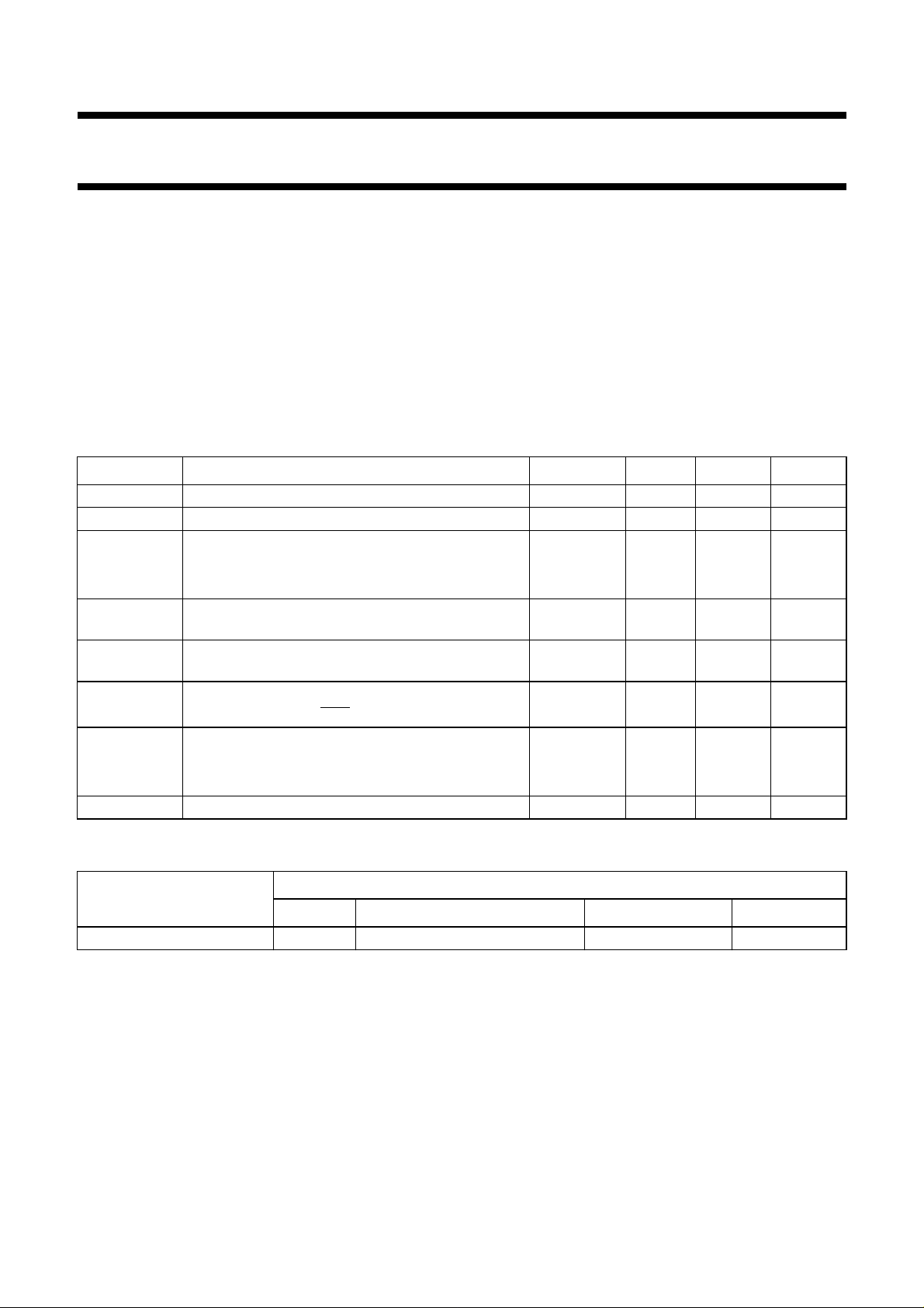
FEATURES
• Adaptive data slicer
• Crystal-controlled data clock regeneration with a bit rate
of 6.9375 MHz
• Adaptive sync separator, horizontal phase detector and
13.5 MHz VCO to provide display phase locked loop
(PLL)
GENERAL DESCRIPTION
The SAA5191 is a bipolar integrated circuit that extracts
teletext data from the video signal (CVBS), regenerates
the teletext clock (TTC) and synchronizes the text display
to the television signals (VCS). This device operates in
conjunction with the Digital Video Teletext (back-end)
Decoder (DVTB - SAA9042A) or any other compatible
device.
• TV synchronization at teletext mode
QUICK REFERENCE DATA
SYMBOL PARAMETER MIN. TYP. MAX. UNIT
V
P
I
P
V
i CVBS
supply voltage (pin 16) − 12 − V
supply current − 70 − mA
CVBS input signal on pin 27 (peak-to-peak value)
at pin 2 LOW − 1 − V
at pin 2 open-circuit − 2.5 − V
V
o
outputs signals TTC and TTD
2.5 3.5 4.5 V
(peak-to-peak value, pins 14, 15)
V
F13
13.5 MHz clock output signal
123V
(peak-to-peak value pin 17)
V
SYNC
video sync output signal (peak-to-peak value, pin 1) −−1V
SYNC output signal
TCS 200 450 650 mV
VCS video composite sync level on output pin 25
LOW −−0.4 V
HIGH 2.4 − 5.5 V
T
amb
operating ambient temperature 0 −+70 °C
ORDERING AND PACKAGE INFORMATION
EXTENDED TYPE
NUMBER
PINS PIN POSITION MATERIAL CODE
PACKAGE
SAA5191 28 DIL plastic SOT117
Note
1. SOT117-1;1996 November 14
March 1991 2
(1)
Page 3
Philips Semiconductors Preliminary specification
Teletext video processor SAA5191
P
(data)
F13
(13.5 MHz
clock)
17
+12 V
P
V
TTD
15
TTC
14
(clock)
12
V
1311978651432
GND
XTAL
MEH149
13.875 MHz
handbook, full pagewidth
VCO
19
PHASE
DETECTOR
HORIZONTAL
PL CBB
P
V
PULSE
GENERATOR
LATCHES
DATA
SLICER
ADAPTIVE
SAA5191
CLOCK
DUAL
BUFFER
POLARITY
PHASE
DETECTOR
PHASE
SENSE
SENSE
"NO LOAD"
SHIFTER
DATA
EXTERNAL
BY 2
DIVIDER
OSCILLATOR
HF LOSS
COMPENSATOR
data
P
V
input
polarity
set sync
Fig.1 Block diagram.
25 24 23 22 10 21 20 18 16
VCS
ADAPTIVE
27
composite
video
input
SYNC
SEPARATOR
28
TCS
SENSE
"NO INPUT"
March 1991 3
set video
input level
GAIN
SWITCH
26
sync output
Page 4

Philips Semiconductors Preliminary specification
Teletext video processor SAA5191
PINNING
SYMBOL PIN DESCRIPTION
STTV 1 sync output signal to TV (positive or negative going)
VILS 2 level select input of video input (LOW equals 1 V)
C
C
C
C
filt
store
ampl
zero
3 video filtering capacitor of HF loss compensation
4 HF storage capacitor
5 amplitude capacitor
6 zero level capacitor
EXD 7 external data current input (note 1)
C
time
C
CLK
8 data timing capacitor for the adaptive data slicer
9 clock phase detector capacitor
CBB 10 blanking insertion input
XTAL 11 13.875 MHz crystal (double of data rate)
CLF 12 6.9375 MHz clock frequency filter
GND 13 ground (0 V)
TTC 14 teletext clock output (for computer controlled teletext)
TTD 15 teletext data output (for computer controlled teletext)
V
P
16 +12 V supply voltage
F13 17 13.5 MHz VCO output (for sandcastle generation)
OSCO 18 oscillator output to series LC-circuit or crystal
C
VCR
19 short time constant capacitor at video recorder mode
(note 2)
OSCI 20 oscillator input from series LC-circuit or crystal
C
hor
21 horizontal phase capacitor / VCR mode
PL 22 sandcastle input (generated in CCT)
R
T
C
T
23 timing resistor for pulse generator
24 timing capacitor for pulse generator
VCS 25 video composite sync output to CCT
C
BL
26 black level capacitor
CVBS 27 composite video input signal from TV
TCS 28 text-composite/scan-composite sync input (TSC/SCS)
PIN CONFIGURATION
page
STTV
1
VILS
2
C
3
filt
C
4
store
C
5
ampl
C
6
zero
EXD
7
SAA5191
8
C
time
C
9
CLK
CCB
10
XTAL
11
CLF
12
GND
13
TTC
MEH150
Fig.2 Pin configuration.
28
27
26
25
24
23
22
21
20
19
18
17
16
1514
TCS
CVBS
C
BL
VCS
C
T
R
T
PL
C
hor
OSCI
C
VCR
OSCO
F13
V
P
TTD
Notes
1. Sliced teletext data from external: active HIGH level (current), low
impedance input.
2. While the loop is locking up.
March 1991 4
Page 5

Philips Semiconductors Preliminary specification
Teletext video processor SAA5191
LIMITING VALUES
In accordance with the Absolute Maximum System (IEC 134).
SYMBOL PARAMETER MIN. MAX. UNIT
V
P
V
5
T
stg
T
amb
CHARACTERISTICS
= 12 V; T
V
P
=25°C and measurements taken in Fig.3, unless otherwise specified.
amb
SYMBOL PARAMETER CONDITIONS MIN. TYP. MAX. UNIT
V
P
I
P
supply voltage range (pin 16) 10.8 12.0 13.2 V
supply current 50 70 105 mA
Video input, sync separator and data slicer
V
i CVBS
input signal sync to white
(peak-to-peak value, pin 27)
sync amplitude (peak-to-peak value) 0.1 − 1V
data slicing level V2= LOW 0.3 0.46 0.7 V
V
2
input voltage LOW (pin 2) 0 − 0.8 V
input voltage HIGH open-circuit equals HIGH 2.0 − 5.5 V
I
2
input current LOW 0 −−150 µA
input current HIGH V
Teletext data output (TTD)
V
22
phase lock pulse (PL) input voltage
(peak-to-peak value, pin 22)
V
o TTD
data output signal on pin 15
(peak-to-peak value)
V
15
C
L
, t
t
r
f
DC output voltage mean level 3 4 5 V
load capacitance on pin 15 −−40 pF
rise and fall time 20 30 45 ns
Teletext clock output (TTC)
V
o TTC
clock output signal on pin 14
(peak-to-peak value)
V
14
C
L
t
, t
r
f
t
d
DC output voltage mean level 3 4 5 V
load capacitance on pin 14 −−40 pF
rise and fall time 20 30 45 ns
delay time of falling edge relative to
other edges of TTD
supply voltage (pin 16) 0 13.2 V
voltage on pin 5 0 5.5 V
storage temperature range −20 125 °C
operating ambient temperature range 0 +70 °C
Z
≤ 250 Ω
S
V2= LOW 0.7 1 1.4 V
V
= HIGH 1.75 2.5 3.5 V
2
V
= HIGH 0.75 1.15 1.75 V
2
< 5.5 V 0 − 1mA
2
phase locked 0 − 3V
phase unlocked 3.9 − 5.5 V
2.5 3.5 4.5 V
2.5 3.5 4.5 V
−−± 20 ns
March 1991 5
Page 6

Philips Semiconductors Preliminary specification
Teletext video processor SAA5191
SYMBOL PARAMETER CONDITIONS MIN. TYP. MAX. UNIT
Text/ scan composite sync input (TCS/SCS)
V
28
I
28
SYNC output buffer
V
o
V
1
I
1
Video composite sync output (VCS)
V
25
I
25
t
d
Horizontal phase detector and 13.5 MHz VCO
V
10
I
10
V
o
V
17
C
L
t
, t
r
f
input voltage LOW for TCS (pin 28) 0 − 0.8 V
input voltage HIGH for
input voltage LOW for
input voltage HIGH for
TCS 2.0 − 7.0 V
SCS 0 − 1.5 V
SCS 3.5 − 7.0 V
input current V28 = 0 to 7 V −40 −70 −100 µA
V
CVBS sync output signal on pin 1
= 10 to V
28
R
= 1.2 kΩ to V
L 1
P
P
−−± 5 µA
−−1V
(peak-to-peak value)
TCS output signal R
DC output voltage at positive sync signal R
DC output voltage at negative sync signal R
= 1.2 kΩ to GND 200 450 650 mV
L 1
= 1.2 kΩ to GND 1.0 1.4 2.0 V
L 1
= 1.2 kΩ to V
L 1
P
9.0 10.1 11.0 V
output current −−±3mA
output voltage LOW (pin 25) 0 − 0.4 V
output voltage HIGH 2.4 − 5.5 V
output current LOW 0 − 0.5 mA
output current HIGH 0 −−1.5 mA
sync separator delay time 250 350 400 ns
input voltage LOW (CBB), pin 10 blanking inserted 0 − 0.5 V
blanking insertion HIGH no blanking 1.0 − 5.5 V
input current −−−5µA
13.5 MHz clock output signal
123V
(peak-to-peak value, pin 17)
DC output voltage maximum swing 4 − 8.5 V
load capacitance on pin 17 −−40 pF
rise and fall time 10 − 30 ns
March 1991 6
Page 7

Philips Semiconductors Preliminary specification
Teletext video processor SAA5191
handbook, full pagewidth
CVBS
sync
data
input
2.2 µF
1.2
kΩ
1.2 kΩ
47 µF
82 Ω
47 nF
+12 V
68
220
68
nF
27 26 25 24 23 22 21 20 19 18 17 16 15
28
12345678
15
video
input
level
select
1
pF
nF
pF
470
pF
kΩ
22
nF
SAA5191
15
µH
9 1011121314
270pF100
(1)(2)
pF
47 nF
3.3 kΩ
47 nF
XTAL
(3)
1 nF
6.8
pF
13.875
MHz
15
pF
470
Ω
15 µF
22 nF
10 nF
VP = 12 V
27
pF
TCS
PL
VCS
F13
TTD
(4)
15
µH
TTC
CBB
XTAL
additional drawing
for crystal application
47
nF
21
13.5
MHz
(2)
47
22
nF
pF
20
19 18
SAA5191
(1) inductance 15 µH at 1 kHz, Co = 2.2 pF. Adjust free-running frequency to 13.5 ±0.1 MHz or apply 13.5 MHz quartz crystal
as shown in additional drawing
−6
(2) Crystal: f = 13.5 MHz (e.g. Philips catalogue number 4322 143 04101); adjustment tolerance±40 × 10
load capacitance C
static parallel capacitance C
Adjust free-running frequency to 13.5 ± 0.5MHz.
(3) Crystal: f = 13.875 MHz; adjustment tolerance ±40× 10
typical resonance resistance R
static parallel capacitance C
= 22 pF; resonance resistance Rr = 22 pF; typical motional capacitance C1 = 23 fF;
L
= 5.5 pF; frequency tolerance ±30× 10−6 in temperature range T = −20 to +70°.
0
−6
= 15 Ω (maximum 60Ω); typical motional capacitance C1 = 19 fF;
r
= 5 pF; frequency tolerance ±30 × 10−6 in temperature range T = −20 to +70°.
o
; load capacitance CL = 15 pF;
;
(4) Coil: Fixed inductance 15 µH ±20%, quality factor Q > 20.
Fig.3 Test circuit and application circuit using LC-circuit or a crystal for VCO (clock F13).
March 1991 7
MEH156
Page 8

Philips Semiconductors Preliminary specification
Teletext video processor SAA5191
PACKAGE OUTLINE
handbook, full pagewidth
DIP28: plastic dual in-line package; 28 leads (600 mil)
SOT117-1
seating plane
L
Z
28
1
pin 1 index
D
A
2
A
A
1
e
b
w M
b
1
15
E
14
c
M
(e )
M
E
1
H
0 5 10 mm
scale
DIMENSIONS (inch dimensions are derived from the original mm dimensions)
A
A
A
UNIT
inches
Note
1. Plastic or metal protrusions of 0.25 mm maximum per side are not included.
max.
mm
OUTLINE
VERSION
SOT117-1
1 2
min.
max.
1.7
1.3
0.066
0.051
IEC JEDEC EIAJ
051G05 MO-015AH
b
b
1
0.53
0.38
0.020
0.014
0.32
0.23
0.013
0.009
REFERENCES
cD E weM
(1) (1)
36.0
35.0
1.41
1.34
March 1991 8
14.1
13.7
0.56
0.54
(1)
92-11-17
95-01-14
Z
max.
1.75.1 0.51 4.0
0.0670.20 0.020 0.16
L
3.9
15.80
3.4
15.24
EUROPEAN
PROJECTION
M
0.62
0.60
H
E
17.15
15.90
0.68
0.63
0.252.54 15.24
0.010.10 0.60
ISSUE DATE
e
1
0.15
0.13
Page 9

Philips Semiconductors Preliminary specification
Teletext video processor SAA5191
SOLDERING
Introduction
There is no soldering method that is ideal for all IC packages. Wave soldering is often preferred when through-hole and
surface mounted components are mixed on one printed-circuit board. However, wave soldering is not always suitable for
surface mounted ICs, or for printed-circuits with high population densities. In these situations reflow soldering is often
used.
This text gives a very brief insight to a complex technology. A more in-depth account of soldering ICs can be found in our
“IC Package Databook”
Soldering by dipping or by wave
The maximum permissible temperature of the solder is 260 °C; solder at this temperature must not be in contact with the
joint for more than 5 seconds. The total contact time of successive solder waves must not exceed 5 seconds.
The device may be mounted up to the seating plane, but the temperature of the plastic body must not exceed the
specified maximum storage temperature (T
be necessary immediately after soldering to keep the temperature within the permissible limit.
(order code 9398 652 90011).
). If the printed-circuit board has been pre-heated, forced cooling may
stg max
Repairing soldered joints
Apply a low voltage soldering iron (less than 24 V) to the lead(s) of the package, below the seating plane or not more
than 2 mm above it. If the temperature of the soldering iron bit is less than 300 °C it may remain in contact for up to
10 seconds. If the bit temperature is between 300 and 400 °C, contact may be up to 5 seconds.
DEFINITIONS
Data sheet status
Objective specification This data sheet contains target or goal specifications for product development.
Preliminary specification This data sheet contains preliminary data; supplementary data may be published later.
Product specification This data sheet contains final product specifications.
Limiting values
Limiting values given are in accordance with the Absolute Maximum Rating System (IEC 134). Stress above one or
more of the limiting values may cause permanent damage to the device. These are stress ratings only and operation
of the device at these or at any other conditions above those given in the Characteristics sections of the specification
is not implied. Exposure to limiting values for extended periods may affect device reliability.
Application information
Where application information is given, it is advisory and does not form part of the specification.
LIFE SUPPORT APPLICATIONS
These products are not designed for use in life support appliances, devices, or systems where malfunction of these
products can reasonably be expected to result in personal injury. Philips customers using or selling these products for
use in such applications do so at their own risk and agree to fully indemnify Philips for any damages resulting from such
improper use or sale.
March 1991 9
 Loading...