

Datasheet SA57000-25D, SA57000-25UK, SA57000-28D, SA57000-28UK, SA57000-29D Datasheet (Philips) [ru]
...Page 1
INTEGRATED CIRCUITS
SA57000-XX
CapFREE 150 mA, low-noise, low dropout
regulator with thermal protection
Product data
Supersedes data of 2003 Apr 30
2003 Jul 30
Page 2
Philips Semiconductors Product data
CapFREE 150 mA, low-noise, low dropout regulator
with thermal protection
GENERAL DESCRIPTION
The CapFREE SA57000 is the first in a new family of unique low
dropout regulators. It needs no external capacitors, offers a low
output noise voltage of 30 µV
of 55 mV @ 50 mA output current. To accommodate high density
layouts, it is packaged in the small footprint 5 leaded SOT23-5 (SO5)
and a 5-bump Wafer Level Chip- Scale package (WL-CSP5). It is ideal
for all portable and cellular phone applications.
Additional features include power and thermal shutdown, output
current limitation, power OK status, thermal warning, and external
logic-controlled on-off via the PWRON pin.
FEATURES
•CapFREE: No output capacitor needed, stable for all capacitive
loads, regardless of ESR
•5 leaded SOT23-5 (SO5) and Wafer Level Chip-Scale (WL-CSP5)
packages
•Low 30 µV
noise without noise bypass capacitor
RMS
•Preset output voltages to 2.5 V, 2.8 V, 2.9 V, 3.0 V, 3.1 V, 3.3 V
and 3.6 V; other voltages available upon request. 2% output
voltage accuracy
•150 mA maximum output current with current limitation
, and an ultra-low dropout voltage
RMS
WL-CSP5 SOT23-5
•Typical dropout voltage 55 mV @ 50 mA output current
•85 µA typical ground current
•Shut-down (standby) current < 1 µA
•Thermal-overload and short-circuit protection
•PWROK pin: both power status and thermal warning indicator
•PWRON pin offers logic-controlled shutdown
•Maximum line regulation: 0.1%/V
•Maximum load regulation: 0.02%/mA.
APPLICA TIONS
•Cordless and mobile phones
•Industrial and medical equipment
•Other battery-powered equipment.
SA57000-XX
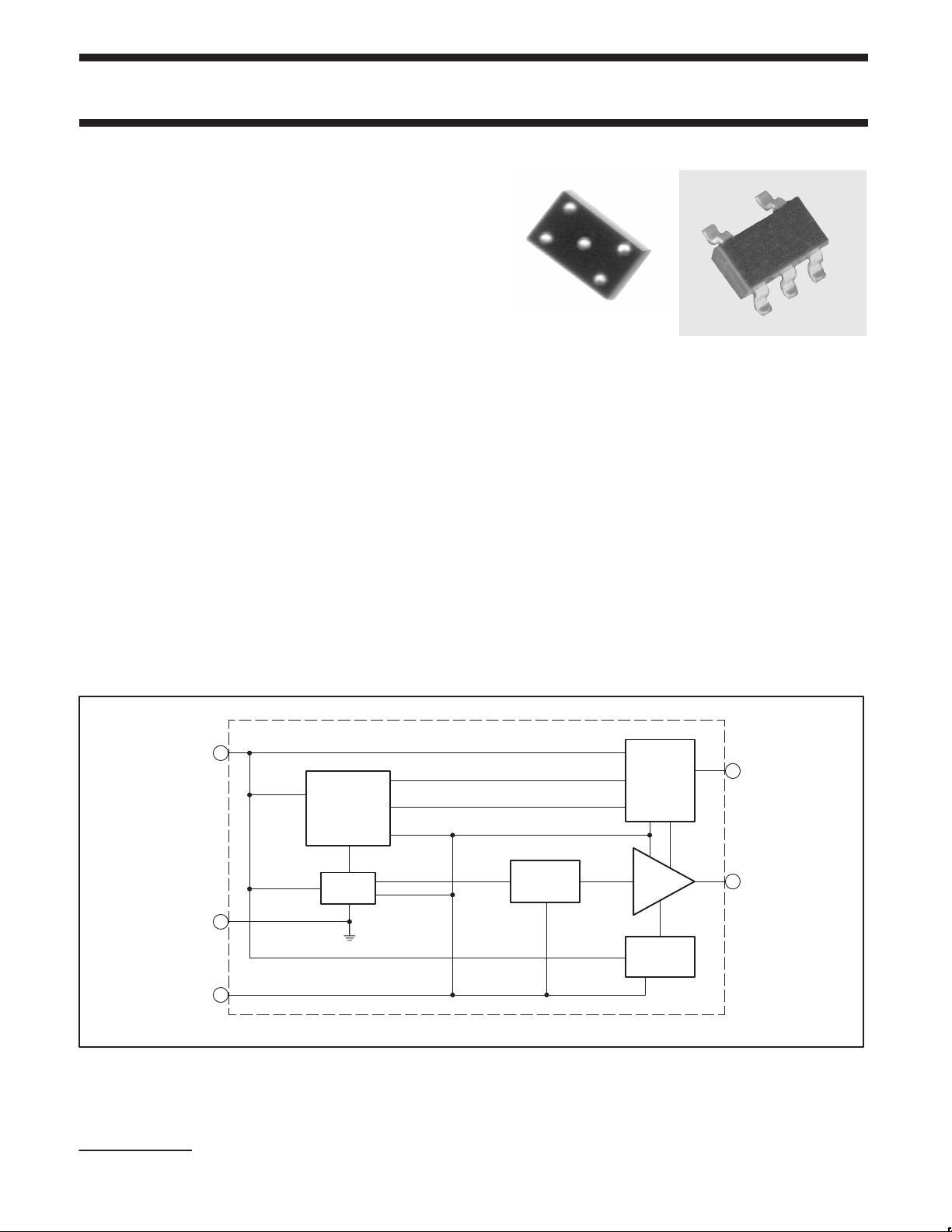
SIMPLIFIED SYSTEM DIAGRAM
GND
V
3
PWRON
PWRON
2
1
IN
PWRON
TEMPERATURE
SENSOR
BAND
GAP
Figure 1. Simplified system diagram.
SA57000
OVER 144 °C (POWER/THERMAL SHUTDOWN)
OVER 127 °C (POWER/THERMAL WARNING)
LOW-PASS
FILTER
PWRON
PWRON
LOGIC
CONTROL
OUTPUT
AMP.
BIAS
NETWORK
SA00557
4
5
PWROK
V
OUT
CapFREE is a trademark of Philips Electronics North America Corporation.
2003 Jul 30
2
Page 3
Philips Semiconductors Product data
TYPE NUMBER
CapFREE 150 mA, low-noise, low dropout regulator
SA57000-XX
with thermal protection
ORDERING INFORMATION
PACKAGE
NAME DESCRIPTION VERSION
SA57000-XXD
SOT23-5,
SO5
plastic small outline package; 5 leads (see dimensional drawing) SOT680-1 –40 to +85 °C
SA57000-XXUK WL-CSP5 wafer level, chip-scale package; 5 bumps (see dimensional drawing) –40 to +85 °C
NOTE:
The device has seven voltage output options, indicated by the XX
on the Type Number.
XX
VOLTAGE (Typical)
25 2.5 V
28 2.8 V
29 2.9 V
30 3.0 V
31 3.1 V
33 3.3 V
36 3.6 V
Marking code
Each device is marked with a four letter code. The first three letters
designate the product. The fourth, represented by an ‘x’, designates
the date tracking code.
Part
SA57000-25UK, SA57000-25D ABKx
SA57000-28UK, SA57000-28D ABLx
SA57000-29UK, SA57000-29D ABXx
SA57000-30UK, SA57000-30D ABMx
SA57000-31UK, SA57000-31D ABYx
SA57000-33UK, SA57000-33D ABNx
SA57000-36UK, SA57000-36D ABPx
TEMPERATURE
RANGE
Marking
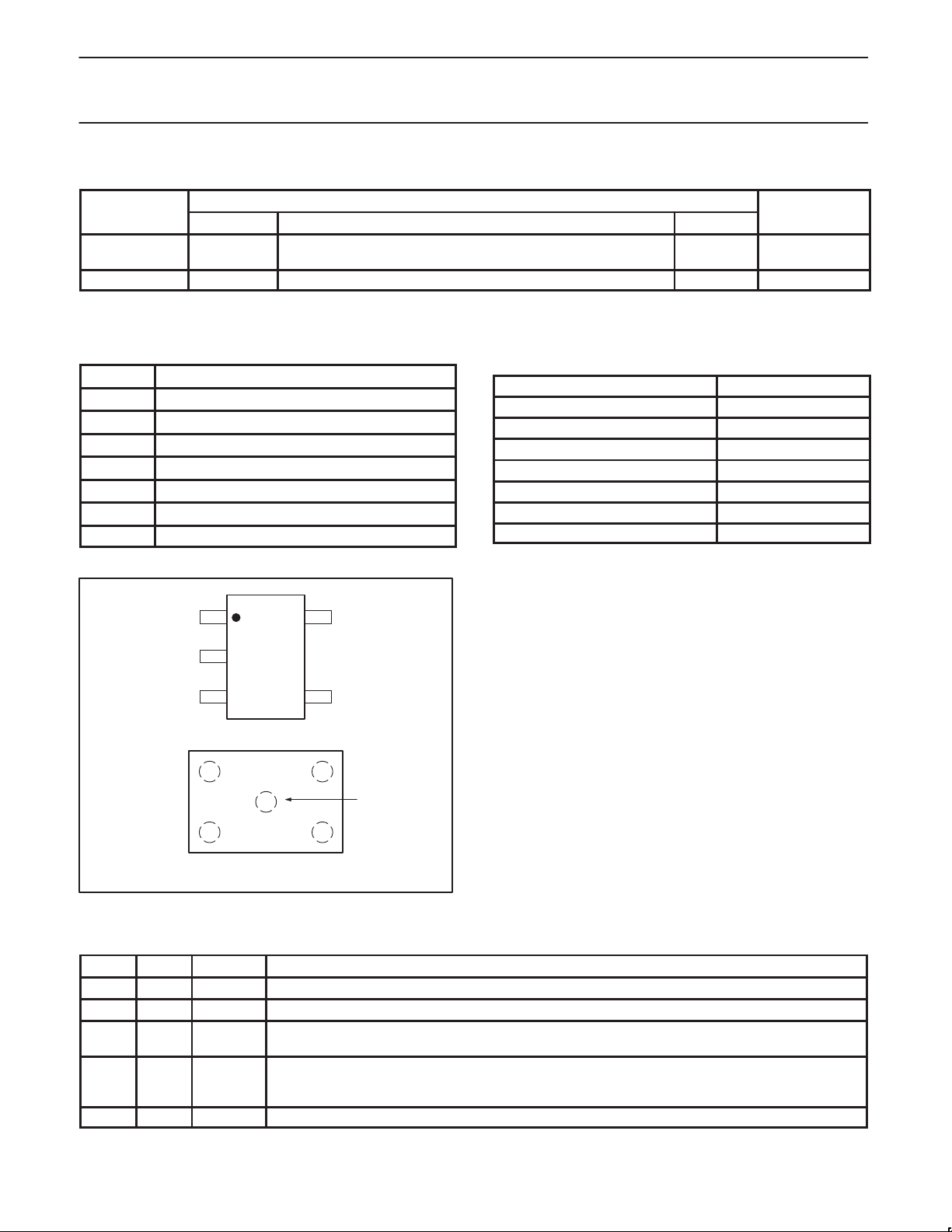
PIN CONFIGURATION
1
V
IN
2
GND
34
TOP VIEW
A3
V
OUT
V
IN
SA57000-XXUK
B2
A1
TOP VIEW
(BALLS ARE ON THE BOTTOM)
Figure 2. Pin configurations.
5V
SA57000-XXD
C3
C1
OUT
PWROKPWRON
PWROK
GND
PWRON
SA00556
PIN DESCRIPTION
PIN BALL SYMBOL DESCRIPTION
1 A1 V
IN
2 B2 GND Ground.
3 C1 PWRON Power-on input. Active-HIGH. A logic LOW powers down the regulator. The shutdown quiescent current is
4 C3 PWROK Power OK indicator, including thermal warning. Connect a 10 kΩ resistor between PWROK and V
5 A3 V
OUT
Regulator input. V
OUT(nom)
+ 0.5 V to 6.5 V. No bypass capacitor required.
typically 50 nA. Connect to VIN for manual operation.
Active-LOW open-drain output indicates an out-of-regulation condition when power falls typically 6% below
VOUT(nom), or thermal warning (trips at 127 °C ± 2 °C).
Regulator output. Sources up to 150 mA. No bypass capacitors required.
OUT
.
2003 Jul 30
3
Page 4
Philips Semiconductors Product data
CapFREE 150 mA, low-noise, low dropout regulator
SA57000-XX
with thermal protection
MAXIMUM RATINGS
SYMBOL PARAMETER CONDITIONS MIN. MAX. UNIT
V
IN
V
PWRON
V
OUT
T
amb
T
j
T
stg
P Power dissipation (Derating factor above 25 °C) T
R
th(j-a)
VIN to GND voltage –0.3 6.5 V
PWRON to GND voltage –0.3 6.5 V
OUT to GND voltage –0.3 VIN + 0.3 V
Operating ambient temperature –40 +85 °C
Junction temperature – +125 °C
Storage temperature –65 +160 °C
= 25 °C – 637 mW
amb
Thermal resistance from junction to ambient – 140 °C/W
DC
DC
DC
2003 Jul 30
4
Page 5
Philips Semiconductors Product data
2
3
4
CapFREE 150 mA, low-noise, low dropout regulator
with thermal protection
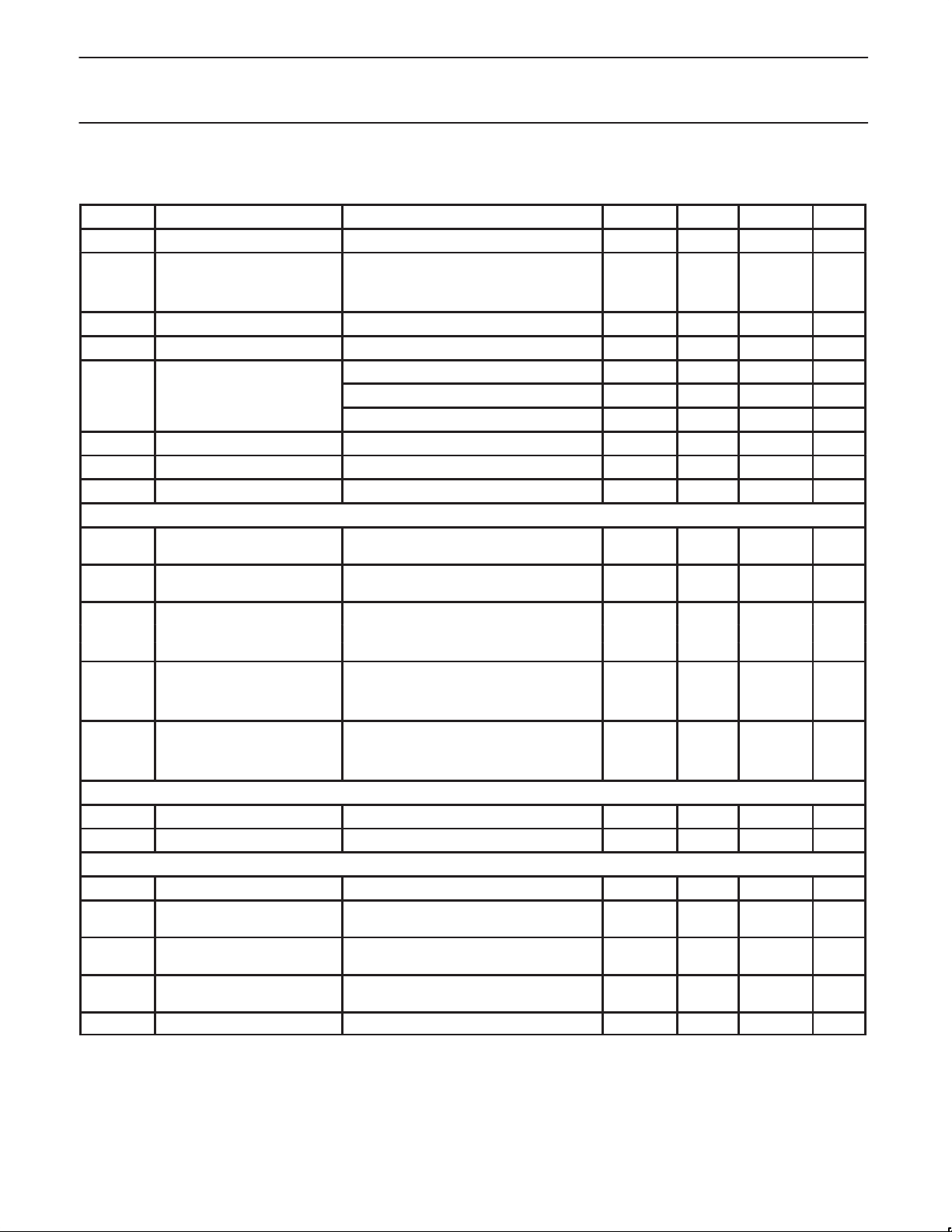
CHARACTERISTICS
VIN = V
OUT(nom)
SYMBOL
V
IN
I
LIM
I
Q
∆V
LNR
∆V
LDR
e
n
Shutdown
V
IH
V
IL
I
PWRON
I
Q(SHDN)
t
PWRON
Thermal protection (Note 2)
T
SHDN
∆T
SHDN
PWROK output (power and temperature OK) (Note 2)
NOTES:
1. Limits are production tested at T
guaranteed by design.
2. Accuracy ±2 °C over temperature range guaranteed by design and characterization.
3. The dropout voltage is defined as V
4. Time needed for V
+ 0.5 V. (Note 1.)
PARAMETER CONDITIONS MIN. TYP. MAX. UNIT
input voltage V
I
output voltage accuracy
–40 °C ≤ T
= 1 mA
OUT
T
= +25 °C – ±1 – %
amb
≤ +85 °C –2.0 – 2.0 %
amb
current limit 160 300 – mA
ground pin current I
dropout voltage
line regulation VIN = (V
load regulation I
output voltage noise f = 10 Hz to 100 kHz, C
PWRON input threshold
(HIGH ON-state)
PWRON input threshold
(HIGH ON-state)
PWRON input bias current
shutdown supply current
power-on start-up time
= 1 mA to 150 mA – 85 150 µA
OUT
I
= 1 mA – 1 – mV
OUT
I
= 50 mA – 55 120 mV
OUT
I
= 150 mA – 165 – mV
OUT
+ 0.1 V) to 5.5 V; I
OUT
= 1 mA to 150 mA – 0.01 0.02 %/mA
OUT
VIN → V
VIN → V
I
= 1 mA, C
OUT
T
OUT(nom)
OUT(nom)
V
PWRON
T
amb
T
amb
V
T
amb
T
amb
T
amb
= –40 to +85 °C – 35 200 µs
amb
→ 6.5 V 0.7 × V
→ 6.5 V – – 0.3 × V
= V
= +25 °C – 0.01 1 µA
= +85 °C – 0.05 – µA
= 0 V
OUT
= +25 °C – 0.05 1 µA
= +85 °C – 0.2 1 µA
OUT
= +25 °C – 25 100 µs
= 20 mA – – 0.1 %/V
OUT
= 10 µF – 30 – µV
OUT
IN
= 100 nF
thermal shut-down temperature – 144 – °C
thermal shut-down hysteresis – 13 – °C
PWROK trip temperature – 127 – °C
PWROK trip temperature
hysteresis
PWROK trip as percentage of
V
OUT(nom)
PWROK hysteresis as
percentage of V
PWROK output (when tripped) I
OUT
OUT(nom)
= +25 °C. All devices are 100% production tested at 25 °C. Limits over the operating tempreature are
amb
– V
to reach 95% of V
IN
,
where V
OUT
OUT(nom)
= 0.5 mA – 0.1 0.4 V
SINK
is 100 mV below the value of V
OUT
.
SA57000-XX
OUT(nom)
IN
– 12 – °C
–3.5 –6 –8 %
– 2 – %
for VIN = V
OUT
– 6.5 V
– – V
+ 0.5 V.
OUT
RMS
V
IN
2003 Jul 30
5
Page 6

Philips Semiconductors Product data
CapFREE 150 mA, low-noise, low dropout regulator
with thermal protection
TYPCIAL PERFORMANCE CURVES
Measurements taken with the SA57000-33 (3.3 volt output).
3.40
I
= 50 mA
LOAD
VIN = V
3.38
3.36
3.34
, OUTPUT VOLTAGE (V)
OUT
V
3.32
3.30
–40 –20 0 20 40 60 80 100
OUT(nom)
+ 0.5 V
T
, TEMPERATURE 〈°C)
amb
Figure 3. Output voltage versus temperature.
SL01515
100
80
60
40
GROUND CURRENT ( A)µ
20
0
–40 –20 0 20 40 60 80 100
Figure 4. Ground current versus temperature.
VIN = V
I
LOAD
OUT(nom)
= 50 mA
+ 0.5 V
T
, TEMPERATURE 〈°C)
amb
SA57000-XX
SL01516
0
–100
–200
–300
–400
GROUND CURRENT ( A)µ
–500
–600
1.0 2.0 3.0 4.0 5.0 6.0
VIN, INPUT VOLTAGE (V)
SL01517
Figure 5. Ground current versus input voltage (no load).
200
150
100
TEMPERATURE ( C)°
Figure 7. Tj versus VIN – V
SHUTDOWN
TEMPERATURE
I = 150 mA
50
T
= +85 °C
amb
0
0 0.5 1.0 1.5 2.0 2.5 3.0
VIN – V
OUT
I = 50 mA
(V)
OUT
for 3 output currents.
I = 100 mA
SL01576
0
LOAD CURRENT = 50 mA
–100
–200
–300
–400
GROUND CURRENT ( A)µ
–500
–600
1.0 2.0 3.0 4.0 5.0 6.0
VIN, INPUT VOLTAGE (V)
SL01518
Figure 6. Ground current versus input voltage with load.
155
150
145
140
, OUTPUT CURRENT (mA)
OUT
135
I
T
= +140 °C
j(max)
= +85 °C
T
amb
130
0 0.5 1.0 1.5 2.0 2.5 3.0
Figure 8. Maximum I
VIN – V
OUT
(V)
OUT
versus VIN – V
OUT
.
SL01577
2003 Jul 30
6
Page 7

Philips Semiconductors Product data
CapFREE 150 mA, low-noise, low dropout regulator
with thermal protection
70
60
50
40
30
PSRR (dB)
20
10
0
0.1 10 1000 100000
FREQUENCY (Hz)
C
= 1 µF
OUT
C
= 0 µF
OUT
SL01873
Figure 9. Power supply rejection ratio versus frequency.
100
µ
10
1
C
= 1 µF
0.1
C
= 0 µF
OUTPUT NOISE SPECTRAL DENSITY ( V/Hz)
0.01
10 100 1000 10000 100000
OUT
FREQUENCY (Hz)
OUT
SL01875
Figure 11. Output noise spectral density versus frequency.
35
C
= 0 µF
OUT
30
)
25
rms
20
15
10
OUTPUT NOISE ( µV
5
0
1 10 100 1000
Figure 10. Output noise versus load current.
90
80
70
60
50
40
LIFETIME IN YEARS
30
20
10
0
0.25
Figure 12. Lifetime versus VIN – V
C
= 0 µF
OUT
LOAD CURRENT (mA)
MTTF = 0.1% failure
at specified lifetime
0.5
VIN – V
SA57000-XX
T
= +85 °C
amb
I = 150 mA
I = 100 mA
I = 50 mA
0.75
(V)
OUT
for 3 output currents.
OUT
SL01874
1
SL01578
2003 Jul 30
7
Page 8

Philips Semiconductors Product data
CapFREE 150 mA, low-noise, low dropout regulator
with thermal protection
TECHNICAL DESCRIPTION
General discussion
The SA57000-XX is a low dropout, low-quiescent current linear
regulator designed primarily for battery-powered applications and
stabilizes with or without input/output capacitors. The device delivers
up to 150 mA and is available with preset output voltages of 2.5 V ,
2.8 V, 2.9 V, 3.0 V, 3.1 V, 3.3 V, and 3.6 V for both SOT 23-5 and
WL-CSP packages.
The 1.23 band-gap reference is connected to the error amplifier’s
inverting input. The error amplifier compares this reference with the
feedback voltage and amplifies the difference. If the feedback
voltage is lower than the reference voltage, the pass-transistor gate
is pulled lower, which allows more current to pass to the output. The
output voltage is fed back through an internal resistor voltage divider
connected to the V
OUT
pin.
Band-gap
The band-gap circuitry generates a temperature independent
voltage by properly adding two voltages with negative and positive
temperature coefficient. The band-gap voltage is typically 1.23 volts
with a temperature variation of 5 mV over the temperature range
from –40 °C to +125 °C.
Low-pass filter
Low-pass filter is basically an RC filter with a low cut-off frequency.
No external capacitor is used. There is one comparator, which
turns on the bypass paths to charge or discharge the capacitor if the
output of the filter is higher or lower than the band-gap voltage by a
specified amount.
Output amplifier
The output amplifier is a folded-cascode PMOS amplifier which
controls the gate of the output transistor and sources the load
current. A portion of the output voltage is compared to the reference
voltage and a constant voltage is maintained at output. The output is
also monitored by a comparator which trips PWROK if the output
voltage falls below the nominal output level by a specified amount
due to low battery condition or any other reason. The current limiter
circuit monitors the output current and limits the load current to a
certain value to avoid any damage due to short circuit.
Bias circuit
The bias block provides bias currents and voltages for the other
blocks. It has a self start-up circuit and it can establish the bias
currents and voltages very fast.
Temperature sensor
The temperature sensor block monitors the die temperature and
flags PWROK when the temperature crosses 125 °C. If the die
temperature goes beyond 144 °C typical value, the output amplifier
is shut down. Both the temperatures corresponding to Power-OK or
shutdown have a hysteresis of 13 °C.
ESD protection
The standard ESD blocks protect the CMOS circuit against
electrostatic discharge (ESD).
PRWROK output
PWROK goes LOW when the output voltage goes out of regulation
as during drop-out, current limit or thermal shutdown. PowerOK is
an open-drain N-channel MOSFET. To obtain a logic-level output,
connect a 10 kΩ pull-up resistor from PWROK pin to V
minimize current consumption, make this resistor as large as
practical. A 100 kΩ resistor works well for most applications. The
PowerOK is not active during shutdown.
Current limit
The SA57000-XX includes a current limiter that monitors and
controls the pass transistor’s gate voltage, limiting the output current
to 300 mA typical value. For design purposes, consider the current
limit to be 160 mA minimum value. The output can be shorted to
ground for an indefinite period of time without damaging the part.
Thermal-overload protection
When the junction temperature exceeds Tj = 144 _C typical value,
the thermal sensor signals the shutdown logic, turning off the output
amplifier and allowing the die to cool. The thermal sensor will turn
the output amplifier on again after the die’s junction temperature
decreases by 13 _C hysteresis value, resulting in a pulsed output
during continuous thermal overload conditions.
SA57000-XX
pin. To
OUT
2003 Jul 30
8
Page 9

Philips Semiconductors Product data
CapFREE 150 mA, low-noise, low dropout regulator
with thermal protection
TIMING DIAGRAM
V
+ 0.5 V
OUT(nom)
V
V
OUT(nom)
IN
–4%
2% HYSTERESIS
–6%
V
OUT(nom)
+ V
DROPOUT
SA57000-XX
PWROK
LOGIC_ON LOGIC_ON LOGIC_ON
LOGIC_OFF LOGIC_OFF
SL01876
Figure 13. Timing diagram.
2003 Jul 30
9
Page 10

Philips Semiconductors Product data
CapFREE 150 mA, low-noise, low dropout regulator
with thermal protection
WL-CSP5: wafer level, chip-scale package; 5 bumps
X3
X4
X5
X1
X6
BUMP
SA57000-XX
X2
X7
DIMENSIONS (mm are the original dimensions)
UNIT X1
mm
1.30
1.24
X2 X3 X4 X5 X6 X7
0.87
0.81
0.5 0.5
0.195
0.165
0.467
0.447
0.145
0.115
SL02055
2003 Jul 30
10
Page 11

Philips Semiconductors Product data
CapFREE 150 mA, low-noise, low dropout regulator
with thermal protection
TAPE & REEL IN WAFER LEVEL CHIP-SCALE PACKAGE
LOADED TAPE DIRECTION OF FEED
NOTES:
All dimensions in millimeters.
10 sprocket hole pitch cumulative tolerance ±0.20
Material: conductive polystyrene
Camber not to exceed 1.0 mm in 100 mm.
Cover tape shown for illustrative purposes only.
P
4.00
2.00 ±0.01
∅1.5
+0.1
+0.0
X
SA57000-XX
1.75
3.50 ±0.01
W
Ao
TOP COVER TAPE
DIMENSIONS (mm are the original dimensions)
UNIT Ao
mm
1.09
0.99
Bo T T1 P W
1.598
1.498
0.76
0.74
0.10
(max.)
4.05
3.95
Heat seal cover tape for carrier tape width 8 mm
Type tape: clear static dissipative tape
Base material: transparent polyester
Cover tape width: 5.3 ± 0.1 mm
Cover tape length: 480 m/reel
Supplier: Advanced Integrated Materials (AIM)
Part Number: CT5–00530–0480
8.3
7.9
CENTER LINES OF CAVITY
BOTTOM
COVER
TAPE
X
T
Bo
T1
T1
SECTION ‘X – X’
BOTTOM
COVER
TAPE
TOP COVER TAPE
2003 Jul 30
SL02056
11
Page 12

Philips Semiconductors Product data
CapFREE 150 mA, low-noise, low dropout regulator
with thermal protection
PACKING METHOD
TAPE
GUARD BAND
BARCODE LABEL
ESD EMBOSSED
PRINTED PLANO BOX
SA57000-XX
REEL ASSEMBLY
PRE-PRINTED HYATT PATENT
PRINTED ESD WARNING
SPACE FOR ADDITIONAL LABEL
BARCODE LABEL
PRINTED PLANO BOX
QA SEAL
SL02060
Figure 14. Tape and reel packing method
2003 Jul 30
12
Page 13

Philips Semiconductors Product data
CapFREE 150 mA, low-noise, low dropout regulator
SA57000-XX
with thermal protection
SO5: plastic small outline package; 5 leads; body width 1.6 mm SOT680-1
2003 Jul 30
13
Page 14

Philips Semiconductors Product data
CapFREE 150 mA, low-noise, low dropout regulator
with thermal protection
REVISION HISTORY
Rev Date Description
_6 20030730 Product data (9397 750 11836); ECN 853-2265 29874 of 28 July 2003;
supersedes data of 2003 Apr 30 (9397 750 11452).
Modifications:
•Add “Marking code” table to page 3.
_5 20030430 Product data (9397 750 11452); ECN 853-2265 29874 of 29 April 2003;
supersedes data of 2003 Apr 01 (9397 750 10539).
_4 20030401 Product data (9397 750 10539); ECN 853–2265 29019 of 07 October 2002;
supersedes data of 2001 Oct 16 (9397 750 08983).
_3 2001 1016 Product data (9397 750 08983); ECN 853-2265 27240 of 16 October 2001.
_2 20010827 Product data (9397 750 08722); ECN 853–2265 26991 of 27 August 2001.
_1 20010712 Product data (9397 750 08564); ECN 853-2265 26703 of 12 July 2001.
SA57000-XX
2003 Jul 30
14
Page 15

Philips Semiconductors Product data
CapFREE 150 mA, low-noise, low dropout regulator
SA57000-XX
with thermal protection
Data sheet status
Product
Level
I
II
III
[1] Please consult the most recently issued data sheet before initiating or completing a design.
[2] The product status of the device(s) described in this data sheet may have changed since this data sheet was published. The latest information is available on the Internet at URL
[3] For data sheets describing multiple type numbers, the highest-level product status determines the data sheet status.
Data sheet status
Objective data
Preliminary data
Product data
http://www.semiconductors.philips.com.
[1]
[2] [3]
status
Development
Qualification
Production
Definitions
This data sheet contains data from the objective specification for product development.
Philips Semiconductors reserves the right to change the specification in any manner without notice.
This data sheet contains data from the preliminary specification. Supplementary data will be published
at a later date. Philips Semiconductors reserves the right to change the specification without notice, in
order to improve the design and supply the best possible product.
This data sheet contains data from the product specification. Philips Semiconductors reserves the
right to make changes at any time in order to improve the design, manufacturing and supply. Relevant
changes will be communicated via a Customer Product/Process Change Notification (CPCN).
Definitions
Short-form specification — The data in a short-form specification is extracted from a full data sheet with the same type number and title. For detailed information see
the relevant data sheet or data handbook.
Limiting values definition — Limiting values given are in accordance with the Absolute Maximum Rating System (IEC 60134). Stress above one or more of the limiting
values may cause permanent damage to the device. These are stress ratings only and operation of the device at these or at any other conditions above those given
in the Characteristics sections of the specification is not implied. Exposure to limiting values for extended periods may affect device reliability.
Application information — Applications that are described herein for any of these products are for illustrative purposes only. Philips Semiconductors make no
representation or warranty that such applications will be suitable for the specified use without further testing or modification.
Disclaimers
Life support — These products are not designed for use in life support appliances, devices, or systems where malfunction of these products can reasonably be
expected to result in personal injury . Philips Semiconductors customers using or selling these products for use in such applications do so at their own risk and agree
to fully indemnify Philips Semiconductors for any damages resulting from such application.
Right to make changes — Philips Semiconductors reserves the right to make changes in the products—including circuits, standard cells, and/or software—described
or contained herein in order to improve design and/or performance. When the product is in full production (status ‘Production’), relevant changes will be communicated
via a Customer Product/Process Change Notification (CPCN). Philips Semiconductors assumes no responsibility or liability for the use of any of these products, conveys
no license or title under any patent, copyright, or mask work right to these products, and makes no representations or warranties that these products are free from patent,
copyright, or mask work right infringement, unless otherwise specified.
Contact information
For additional information please visit
http://www.semiconductors.philips.com . Fax: +31 40 27 24825
For sales offices addresses send e-mail to:
sales.addresses@www.semiconductors.philips.com.
Document order number: 9397 750 11836
Koninklijke Philips Electronics N.V. 2003
All rights reserved. Printed in U.S.A.
Date of release: 07-03
2003 Jul 30
15
Page 16

 Loading...