

Page 1

INTEGRATED CIRCUITS
74F543
Octal registered transceiver,
non-inverting (3-State)
74F544
Octal registered transceiver,
inverting (3-State)
Product specification 1994 Dec 5
IC15 Data Handbook
Philips Semiconductors
Page 2
Philips Semiconductors Product specification
74F543
74F543
74F544
74F543, 74F544Octal registered transceivers
74F543 Octal registered transceiver, non-inverting (3-State)
74F544 Octal registered transceiver, inverting 93-State)
FEA TURES
•Combines74F245 and 74F373 type functions in one chip
•8-bit octal transceiver with D-type latch
•74F543 Non-inverting
74F544 Inverting
•Back-to-back registers for storage
•Separate controls for data flow in each direction
•A outputs sink 20mA and source 3mA
•B outputs sink 64mA and source 15mA
•3-State outputs for bus-oriented applications
•74F543 available in SSOP Type II package
DESCRIPTION
The 74F543 and 74F544 Octal Registered Transceivers contain two
sets of D-type latches for temporary storage of data flowing in either
direction. Separate Latch Enable (LEAB
, OEBA) inputs are provided for each register to permit
(OEAB
independent control of inputting and outputting in either direction of
data flow. While the 74F543 has non-inverting data path, the 74F544
inverts data in both directions. The A outputs are guaranteed to sink
24mA, while the B outputs are rated for 64mA.
ORDERING INFORMATION
DESCRIPTION
24-pin plastic skinny DIP (300mil)
24-pin plastic SOL
24-pin plastic SSOP Type II 74F543DB SOT340-1
, LEBA) and Output Enable
COMMERCIAL RANGE
V
T
A
CC
= 0°C to +70°C
N74F543N,
N74F544N
N74F543D,
N74F544D
FUNCTIONAL DESCRIPTION
The 74F543 and 74F544 contain two sets of eight D-type latches,
with separate input and controls for each set. For data flow from A to
B, for example, the A-to-B Enable (EAB
to enter data from A0 - A7 or take data from B0 - B7, as indicated in
the Function Table. With EAB
Enable (LEAB
subsequent Low-to-High transition for the LEAB
A latches in the storage mode and their outputs no longer change
with the A inputs. With EAB
B output buffers are active and display the data present at the
outputs of the A latches. Control of data flow from B to A is similar,
but using the EBA
TYPE
74F543 6.0ns 80mA
74F544 6.5ns 95mA
= 5V ±10%,
) input makes the A-to-B latches transparent; a
, LEBA, and OEBA inputs.
TYPICAL
PROPAGATION
Low, a Low signal on the A-to-B Latch
and OEAB both Low, the 3-State
DELA Y
) input must be Low in order
signal puts the
TYPICAL
SUPPLY CURRENT
(TOTAL)
DRAWING
NUMBER
SOT222–1
SOT137-1
INPUT AND OUTPUT LOADING AND FAN-OUT TABLE
PINS DESCRIPTION
A0 - A7 Port A, 3-State inputs 3.5/1.0 70µA/0.6mA
B0 - B7 Port B, 3-State inputs 3.5/1.0 70µA/0.6mA
OEAB A-to-B Output Enable input (Active Low) 1.0/1.0 20µA/0.6mA
74F543
74F544
NOTE: One (1.0) FAST Unit Load is defined as: 20µA in the High State and 0.6mA in the Low state.
1994 Dec 5 853-0874 14379
OEBA B-to-A Output Enable input (Active Low) 1.0/1.0 20µA/0.6mA
EAB A-to-B Enable input (Active Low) 1.0/2.0 20µA/1.2mA
EBA B-to-A Enable input (Active Low) 1.0/2.0 20µA/1.2mA
LEAB A-to-B Latch Enable input (Active Low) 1.0/1.0 20µA/0.6mA
LEBA B-to-A Latch Enable input (Active Low) 1.0/1.0 20µA/0.6mA
A0 - A7 Port A, 3-State outputs 150/40 3.0mA/24mA
B0 - B7 Port B, 3-State outputs 750/106.7 15mA/64mA
A0 - A7 Port A, 3-State outputs 150/40 3.0mA/24mA
B0 - B7 Port B, 3-State outputs 750/106.7 15mA/64mA
2
74F(U.L.)
HIGH/LOW
LOAD VALUE
HIGH/LOW
Page 3
Philips Semiconductors Product specification
74F543, 74F544Octal registered transceivers
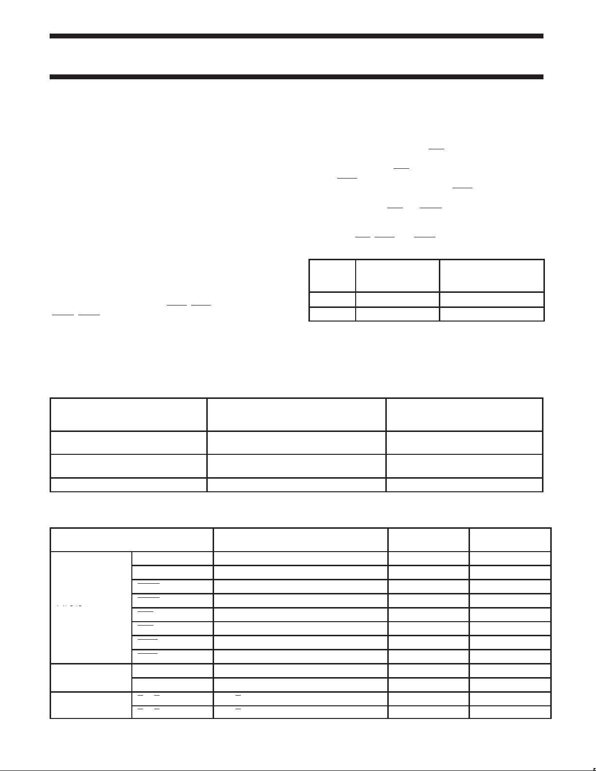
PIN CONFIGURATION – 74F543
LEBA
1
OEBA
2
3
A0
4
A1
5
A2
6
A3
7
A4
8
A5
9
A6
10
A7
EAB LEAB
11
GND
24
V
EBA
23
22
B0
21
B1
20
B2
19
B3
18
B4
17
B5
16
B6
15
B7
14
OEAB
1312
SF00237
CC
LOGIC SYMBOL (IEEE/IEC) – 74F543
2
23
1
13
11
14
IEN3
G1
1C5
2EN4
G2
2C6
LOGIC SYMBOL – 74F543
345678910
A0 A1 A2 A3 A4 A5 A6 A7
EAB
11
23
EBA
LEAB
14
LEBA
1
B0 B1 B2 B3 B4 B5 B6 B7
= Pin 24
V
CC
GND = Pin 12
22 21 20 19 18 17 16 15
OEAB
OEBA
13
2
SF00238
3
4
5
6
7
8
9
10
35D
46D
22
21
20
19
18
17
16
15
SF00239
1994 Dec 5
3
Page 4
Philips Semiconductors Product specification
Disable +
Latch +
Transparent
74F543, 74F544Octal registered transceivers
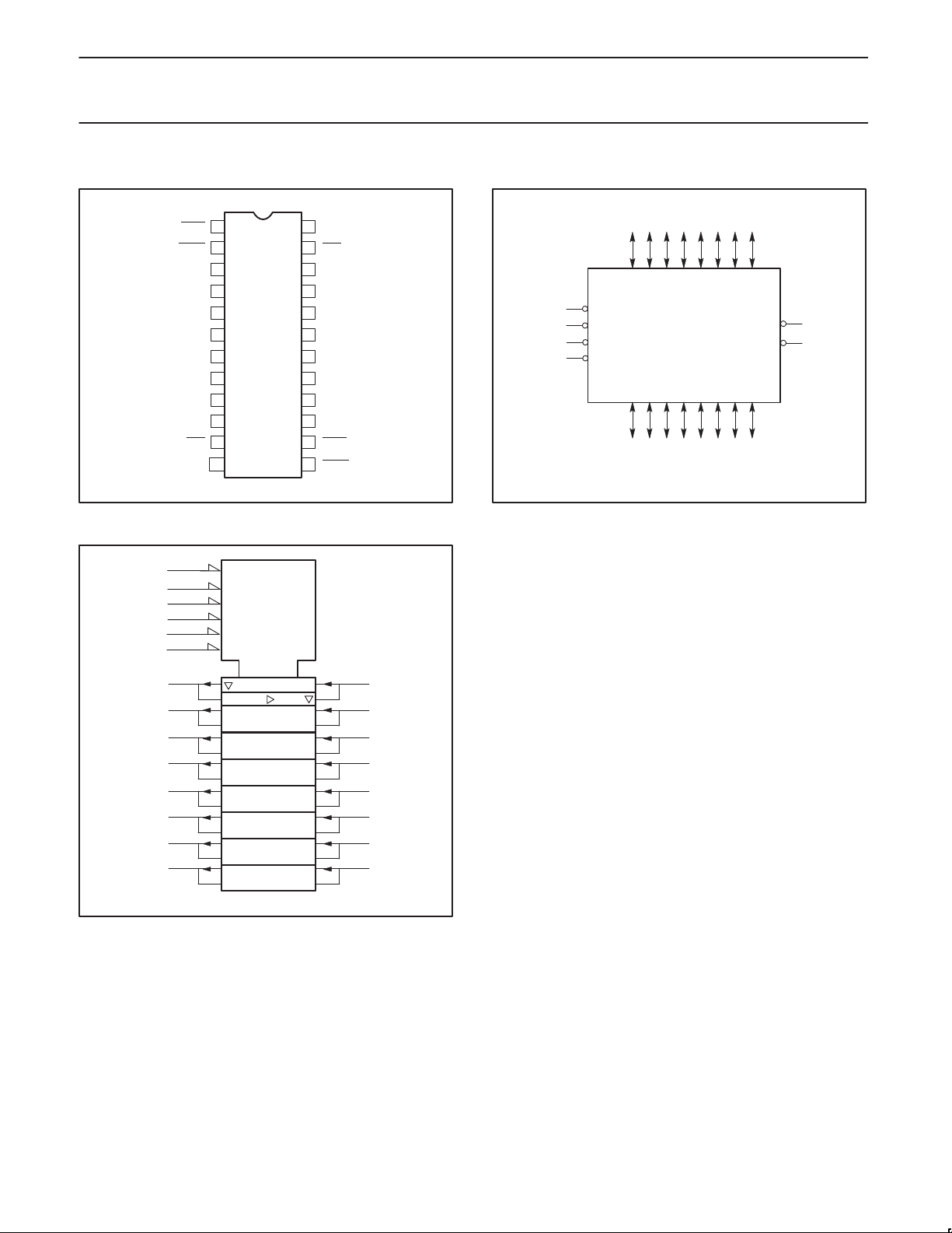
PIN CONFIGURATION – 74F544
LEBA
1
OEBA
2
3
A
0
4
A
1
5
2
A
6
A3
7
A
4
8
5
A
9
A
6
10
7
A
EAB LEAB
11
GND
24
V
EBA
23
22
B0
21
B
20
B
19
B3
18
B
17
B
16
B
15
B
14
OEAB
1312
SF00240
CC
1
2
4
5
6
7
LOGIC SYMBOL (IEEE/IEC) – 74F544
2
23
1
13
11
14
3
4
5
6
7
8
9
10
IEN3
G1
1C5
2EN4
G2
2C6
35D
46D
SF00241
LOGIC SYMBOL – 74F544
345678910
A0 A1 A2 A3 A4 A5 A6 A7
EAB
11
23
14
1
= Pin 24
V
CC
GND = Pin 12
EBA
LEAB
LEBA
B0 B1 B2 B3 B4 B5 B6 B7
22 21 20 19 18 17 16 15
OEAB
OEBA
13
2
SF00242
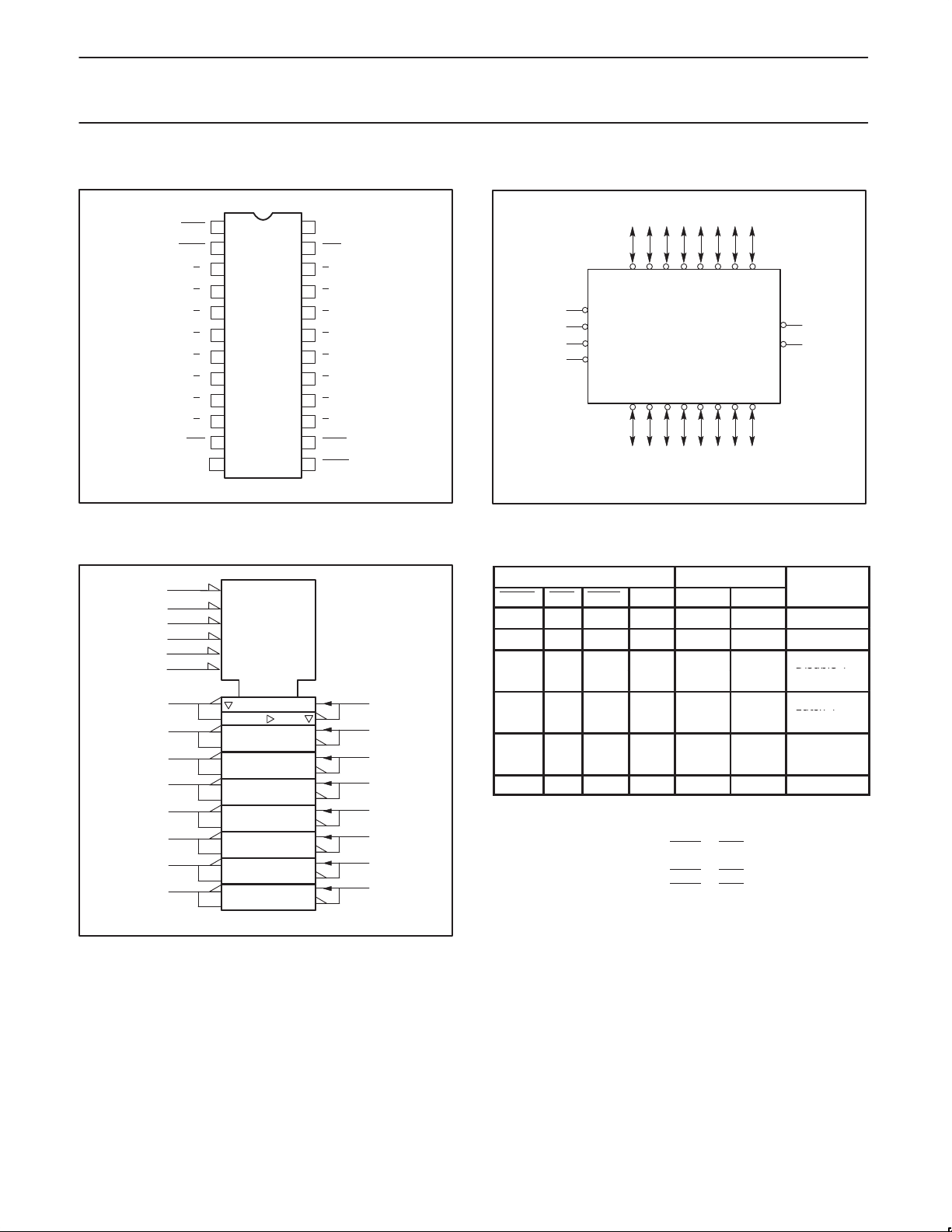
FUNCTION TABLE for 74F543 and 74F544
INPUTS OUTPUTS STATUS
OEXX EXX LEXX DATA 74F543 74F544
H X X X Z Z Disabled
X H X X Z Z Disabled
L ↑ L h Z Z
L ↑ L l Z Z
22
21
20
L L ↑ h H L
L L ↑ l L H
L L L H H L
L L L L L H
19
18
17
16
15
L L H X NC NC Hold
H = High voltage level
L = Low voltage level
h = High state must be present one setup time before the
Low-to-High transition of LEXX
or EXX (XX=AB or BA)
l = Low state must be present one setup time before the
Low-to-High transition of LEXX
↑ = Low-to-High transition of LEXX
or EXX (XX=AB or BA)
or EXX XX = AB or BA
X = Don’t care
NC = No change
Z = High impedance “off” state
Disable +
Latch
Latch +
Display
p
1994 Dec 5
4
Page 5
Philips Semiconductors Product specification
74F543, 74F544Octal registered transceivers
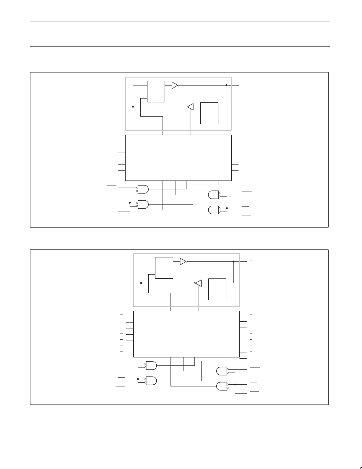
LOGIC DIAGRAM FOR 74F543
OEBA
EBA
VCC = Pin 24
GND = Pin 12
LEBA
LOGIC DIAGRAM FOR 74F544
QD
LE
3
A0
4
A1
5
A2
6
A3
7
A4
8
A5
9
A6
10
A7
2
23
1
DETAIL A X 7
DETAIL A
QD
LE
22
B0
21
B1
20
B2
19
B3
18
B4
17
B5
16
B6
15
B7
13
OEAB
11
EAB
14
LEAB
SF00243
VCC = Pin 24
GND = Pin 12
OEBA
EBA
LEBA
QD
LE
3
0
A
4
A
1
5
A
2
6
A
3
7
4
A
8
A
5
9
6
A
10
A
7
2
23
1
DETAIL A X 7
DETAIL A
QD
LE
22
B0
21
B
20
B
19
B
18
B
17
B
16
B
15
B
13
OEAB
11
EAB
14
LEAB
SF00244
1
2
3
4
5
6
7
1994 Dec 5
5
Page 6

Philips Semiconductors Product specification
I
Current applied to output in Low output state
SYMBOL
PARAMETER
UNIT
IOHHigh-level output current
IOLLow-level output current
74F543, 74F544Octal registered transceivers
ABSOLUTE MAXIMUM RATINGS
(Operation beyond the limits set forth in this table may impair the useful life of the device. Unless otherwise noted these limits are over the
operating free-air temperature range.)
SYMBOL PARAMETER RATING UNIT
V
CC
V
IN
I
IN
V
OUT
OUT
T
amb
T
STG
RECOMMENDED OPERATING CONDITIONS
V
CC
V
IH
V
IL
I
IK
T
amb
Supply voltage -0.5 to +7.0 V
Input voltage -0.5 to +7.0 V
Input current -30 to +5 mA
Voltage applied to output in High output state -0.5 to +5.5 V
pp
p
p
Operating free-air temperature range 0 to +70
Storage temperature -65 to +150
A0 - A7, A0 - A7 48 mA
B0 - B7, B0 - B7 128 mA
°
°
LIMITS
MIN NOM MAX
Supply voltage 4.5 5.0 5.5 V
High-level input voltage 2.0 V
Low-level input voltage 0.8 V
Input clamp current -18 mA
p
p
Operating free-air temperature range -0 +70
A0 - A7, A0 - A7 -3 mA
B0 - B7, B0 - B7 -15 mA
A0 - A7, A0 - A7 24 mA
B0 - B7, B0 - B7 64 mA
°
C
C
C
1994 Dec 5
6
Page 7

Philips Semiconductors Product specification
1
SYMBOL
PARAMETER
TEST CONDITIONS
1
UNIT
V
MIN
I
3mA
VOHHigh-level out ut voltage
V
IL
MAX
V
IH
MIN
I
15mA
V
MIN
I
24mA
VOLLow-level out ut voltage
V
IL
MAX
V
IH
MIN
I
64mA
I
3
IOSShort-circuit out ut current
3
V
MAX
ICCSu ly current (total)
74F543, 74F544Octal registered transceivers
DC ELECTRICAL CHARACTERISTICS
(Over recommended operating free-air temperature range unless otherwise noted.)
LIMITS
MIN TYP2MAX
A0 - A7,
A0 - A7
p
B0 - B7,
B0 - B7
A0 - A7,
A0 - A7
p
B0 - B7,
B0 - B7
V
Input clamp voltage VCC = MIN, II = I
IK
Input current at maximum
I
input voltage
I
High-level input current VCC = MAX, VI = 2.7V 20 µA
IH
OEAB, OEBA, EAB VCC = MAX, VI = 7.0 V 100 µA
Others VCC = 5.5, VI = 5.5V 1 mA
V
V
CC
=
= MIN
CC
=
= MIN
=
=
OH
OH
OL
OL
= -
= -
=
=
IK
10%V
5%V
10%V
5%V
10%V
5%V
10%V
5%V
2.4
CC
2.7 3.4 V
CC
2.0 V
CC
2.0 V
CC
CC
CC
CC
CC
0.35 0.50 V
0.35 0.50 V
0.42 0.55 V
–0.73 –1.2 V
0.55 V
Others –0.6 mA
I
Low-level input current
IL
EAB,
VCC = MAX, VI = 0.5V
–1.2 mA
EBA
I
+ IIHOff-state output current, high-level voltage applied VCC= MAX, VO = 2.7V 70 µA
OZH
I
+ IILOff-state output current, Low-level voltage applied VCC= MAX, VO = 0. 5V –600 µA
OZH
A0 - A7,
p
A0 - A7
B0 - B7,
CC
=
–60 –150 mA
–100 –225 mA
B0 - B7
pp
74F543
74F544
I
CCH
I
CCL
I
CCZ
I
CCH
I
CCL
I
CCZ
VCC = MAX
VCC = MAX
70 105 mA
95 135 mA
95 135 mA
80 110 mA
105 140 mA
100 135 mA
NOTES:
1. For conditions shown as MIN or MAX, use the appropriate value specified under the recommended operating conditions for the applicable
type.
2. All typical values are at V
3. Not more than one output should be shorted at a time. For testing I
techniques are preferable in order to minimize internal heating and more accurately reflect operational values. Otherwise, prolonged shorting
= 5V, T
CC
amb
= 25°C.
, the use of high-speed test apparatus and/or sample-and-hold
OS
of a High output may raise the chip temperature well above normal and thereby cause invalid readings in other parameter tests. In any
sequence of parameter tests, I
tests should be performed last.
OS
V
1994 Dec 5
7
Page 8

Philips Semiconductors Product specification
SYMBOL
PARAMETER
TEST CONDITIONS
UNIT
SYMBOL
PARAMETER
TEST CONDITIONS
UNIT
74F543, 74F544Octal registered transceivers
AC ELECTRICAL CHARACTERISTICS FOR 74F543
74F543 LIMITS
T
t
PLH
t
PHL
t
PLH
t
PHL
t
PLH
t
PHL
t
PLH
t
PHL
t
PZH
t
PZL
t
PHZ
t
PLZ
t
PZH
t
PZL
t
PHZ
t
PLZ
Propagation delay
An to B
n
Propagation delay
Bn to A
n
Propagation delay
LEBA to A
n
Propagation delay
LEAB to B
n
Output Enable time
OEBA to An or OEAB to B
Output Disable time
OEBA to An or OEAB to B
Output Enable time
EBA to An or EAB to B
n
Output Disable time
EBA to An or EAB to B
n
Waveform 2
Waveform 2
Waveform NO TAG, 2
Waveform NO TAG, 2
Waveform 4
n
Waveform 5
Waveform 4
n
Waveform 5
Waveform 4
Waveform 5
Waveform 4
Waveform 5
= +25°C T
amb
VCC = 5.0V VCC = 5.0V ± 10%
CL = 50pF
RL = 500Ω
MIN TYP MAX MIN MAX
3.5
3.0
2.5
2.5
5.0
4.0
6.0
4.5
2.0
3.5
1.0
1.5
4.5
5.0
2.5
4.5
5.5
5.0
4.0
4.5
7.0
6.0
8.5
6.5
4.0
5.0
3.0
4.0
7.0
7.0
5.0
7.0
8.5
8.0
7.0
7.5
10.0
9.0
11.5
9.5
7.5
8.5
6.5
7.5
10.5
10.5
8.5
11.0
= 0°C to +70°C
amb
CL = 50pF
RL = 500Ω
3.0
2.5
2.5
2.5
4.5
4.0
5.5
4.0
1.5
3.0
1.0
1.0
4.0
4.5
2.0
3.0
9.0
8.5
7.5
8.0
11.0
9.5
12.5
10.0
8.0
9.0
7.5
8.5
11.5
11.0
9.5
12.0
ns
ns
ns
ns
ns
ns
ns
ns
AC SETUP REQUIREMENTS FOR 74F543
74F543 LIMITS
T
= +25°C T
amb
VCC = 5.0V VCC = 5.0V ± 10%
CL = 50pF
RL = 500Ω
MIN TYP MIN MAX
ts(H)
ts(L)
th(H)
th(L)
ts(H)
ts(L)
th(H)
th(L)
Setup time, High or Low
An to LEAB or Bn to LEBA
Hold time, High or Low
An to LEAB or Bn to LEBA
Setup time, High or Low
An to EAB or Bn to EBA
Hold time, High or Low
An to EAB or Bn to EBA
Waveform 3
Waveform 3
0.0
2.5
0.0
1.5
Waveform 3 1.0
2.5
Waveform 3 0.0
1.5
tw(L) Latch enable pulse width, Low W aveform 3 4.0 4.5 ns
= 0°C to +70°C
amb
CL = 50pF
RL = 500Ω
0.0
3.0
0.0
2.0
1.5
3.0
0.0
2.0
ns
ns
ns
ns
1994 Dec 5
8
Page 9

Philips Semiconductors Product specification
SYMBOL
PARAMETER
TEST CONDITIONS
UNIT
SYMBOL
PARAMETER
TEST CONDITIONS
UNIT
74F543, 74F544Octal registered transceivers
AC ELECTRICAL CHARACTERISTICS FOR 74F544
74F544 LIMITS
T
t
PLH
t
PHL
t
PLH
t
PHL
t
PLH
t
PHL
t
PZH
t
PZL
t
PHZ
t
PLZ
t
PZH
t
PZL
t
PHZ
t
PLZ
Propagation delay
An to Bn or Bn to A
n
Propagation delay
LEBA to A
n
Propagation delay
LEAB to B
n
Output Enable time
OEBA to An or OEAB to B
Output Disable time
OEBA to An or OEAB to B
Output Enable time
EBA to An or EAB to B
n
Output Disable time
EBA to An or EAB to B
n
Waveform NO TAG
Waveform NO TAG, 2
Waveform NO TAG, 2
Waveform 4
n
Waveform 5
Waveform 4
n
Waveform 5
Waveform 4
Waveform 5
Waveform 4
Waveform 5
= +25°C T
amb
VCC = 5.0V VCC = 5.0V ± 10%
CL = 50pF
RL = 500Ω
MIN TYP MAX MIN MAX
3.0
3.0
4.0
4.0
5.0
4.0
2.0
3.5
1.0
1.5
4.0
4.5
2.5
4.5
6.5
5.0
7.0
7.0
8.0
7.5
4.0
5.5
4.0
4.0
7.0
8.0
5.0
8.5
9.5
8.0
9.5
9.5
11.5
9.5
7.0
8.5
6.5
6.5
9.5
11.0
8.0
11.5
= 0°C to +70°C
amb
CL = 50pF
RL = 500Ω
3.0
3.0
4.0
4.0
4.0
4.0
1.5
3.0
1.0
1.5
3.5
4.5
2.5
4.0
10.5
8.5
10.5
10.5
12.5
10.5
7.5
9.0
7.0
7.5
10.0
12.0
9.0
11.5
ns
ns
ns
ns
ns
ns
ns
AC SETUP REQUIREMENTS FOR 74F544
74F544 LIMITS
T
= +25°C T
amb
VCC = 5.0V VCC = 5.0V ± 10%
CL = 50pF
RL = 500Ω
MIN TYP MIN MAX
ts(H)
ts(L)
th(H)
th(L)
ts(H)
ts(L)
th(H)
th(L)
Setup time, High or Low
An to LEAB or Bn to LEBA
Hold time, High or Low
An to LEAB or Bn to LEBA
Setup time, High or Low
An to EAB or Bn to EBA
Hold time, High or Low
An to EAB or Bn to EBA
Waveform 3
Waveform 3
Waveform 3
Waveform 3
1.5
1.5
1.5
2.0
1.5
1.5
1.5
2.0
tw(L) Latch enable pulse width, Low W aveform 3 4.0 4.5 ns
= 0°C to +70°C
amb
CL = 50pF
RL = 500Ω
2.0
2.5
2.5
2.5
2.5
2.5
2.0
2.0
ns
ns
ns
ns
1994 Dec 5
9
Page 10

Philips Semiconductors Product specification
74F543, 74F544Octal registered transceivers
AC WAVEFORMS
V
= 1.5V
M
The shaded areas indicate when the input is permitted to change for predictable output performance.
OEAB, OEBA
V
V
IN
OUT
t
PHL
EAB, EBA
V
M
V
V
M
t
PLH
B
M
V
M
A
n
n,
A
B
n,
n
V
t
M
PZH
V
M
t
PHZ
V
M
VOH -0.3V
0V
SF00245
Waveform 1. Propagation Delay for Inverting Outputs
V
V
OUT
V
t
PLH
M
V
IN
V
M
t
PHL
V
M
M
SF00246
Waveform 2. Propagation Delay for Non-Inverting Outputs
A
n
B
n
A
n
B
n
LEAB, LEBA
EAB, EBA
ts(H)
V
V
M
M
t
(H)
h
V
M
V
V
M
M
(L)
t
s
tw(L)
th(L)
V
M
SF00247
Waveform 3. Data Setup Time and Hold Times, and Latch
Enable Pulse Width
SF00248
Waveform 4. 3-State Output Enable Time to High Level and
Output Disable Time from High Level
OEAB, OEBA
EAB, EBA
A
n,
A
n,
B
n
B
n
V
t
PZL
M
V
V
M
t
PLZ
M
VOL +0.3V
SF00249
Waveform 5. 3-State Output Enable Time to Low Level and
Output Disable Time from Low Level
1994 Dec 5
10
Page 11

Philips Semiconductors Product specification
74F543, 74F544Octal registered transceivers
TEST CIRCUIT AND WAVEFORMS
V
CC
PULSE
GENERATOR
V
IN
R
T
D.U.T.
V
OUT
Test Circuit for Open Collector Outputs
SWITCH POSITION
TEST SWITCH
t
PLZ
t
PZL
closed
closed
All other open
7.0V
R
L
C
R
L
L
NEGATIVE
PULSE
POSITIVE
PULSE
90%
10%
V
M
10%
t
THL (tf
t
TLH (tr
90%
V
M
Input Pulse Definition
t
w
V
M
10%
)
)
t
)
TLH (tr
t
)
THL (tf
90%
V
M
t
w
90%
10%
AMP (V)
0V
AMP (V)
0V
DEFINITIONS:
= Load resistor;
R
L
see AC electrical characteristics for value.
C
= Load capacitance includes jig and probe capacitance;
L
see AC electrical characteristics for value.
R
= Termination resistance should be equal to Z
T
pulse generators.
OUT
of
family
74F
INPUT PULSE REQUIREMENTS
V
amplitude
3.0V
M
1.5V
rep. rate
1MHz 500ns
t
w
t
TLHtTHL
2.5ns 2.5ns
SF00128
1994 Dec 5
11
Page 12

Philips Semiconductors Product specification
74F543, 74F544Bus transceivers
DIP24: plastic dual in-line package; 24 leads (300 mil) SOT222-1
1994 Dec 05
12
Page 13

Philips Semiconductors Product specification
74F543, 74F544Bus transceivers
SO24: plastic small outline package; 24 leads; body width 7.5 mm SOT137-1
1994 Dec 05
13
Page 14

Philips Semiconductors Product specification
74F543, 74F544Bus transceivers
SSOP24: plastic shrink small outline package; 24 leads; body width 5.3 mm SOT340-1
1994 Dec 05
14
Page 15

Philips Semiconductors Product specification
74F543, 74F544Bus transceivers
NOTES
1994 Dec 05
15
Page 16

Philips Semiconductors Product specification
74F543, 74F544Octal registered transceivers
DEFINITIONS
Data Sheet Identification Product Status Definition
Objective Specification
Preliminary Specification
Product Specification
Formative or in Design
Preproduction Product
Full Production
Philips Semiconductors and Philips Electronics North America Corporation reserve the right to make changes, without notice, in the products,
including circuits, standard cells, and/or software, described or contained herein in order to improve design and/or performance. Philips
Semiconductors assumes no responsibility or liability for the use of any of these products, conveys no license or title under any patent, copyright,
or mask work right to these products, and makes no representations or warranties that these products are free from patent, copyright, or mask
work right infringement, unless otherwise specified. Applications that are described herein for any of these products are for illustrative purposes
only. Philips Semiconductors makes no representation or warranty that such applications will be suitable for the specified use without further testing
or modification.
LIFE SUPPORT APPLICA TIONS
Philips Semiconductors and Philips Electronics North America Corporation Products are not designed for use in life support appliances, devices,
or systems where malfunction of a Philips Semiconductors and Philips Electronics North America Corporation Product can reasonably be expected
to result in a personal injury. Philips Semiconductors and Philips Electronics North America Corporation customers using or selling Philips
Semiconductors and Philips Electronics North America Corporation Products for use in such applications do so at their own risk and agree to fully
indemnify Philips Semiconductors and Philips Electronics North America Corporation for any damages resulting from such improper use or sale.
Philips Semiconductors
811 East Arques Avenue
P.O. Box 3409
Sunnyvale, California 94088–3409
Telephone 800-234-7381
This data sheet contains the design target or goal specifications for product development. Specifications
may change in any manner without notice.
This data sheet contains preliminary data, and supplementary data will be published at a later date. Philips
Semiconductors reserves the right to make changes at any time without notice in order to improve design
and supply the best possible product.
This data sheet contains Final Specifications. Philips Semiconductors reserves the right to make changes
at any time without notice, in order to improve design and supply the best possible product.
Philips Semiconductors and Philips Electronics North America Corporation
register eligible circuits under the Semiconductor Chip Protection Act.
Copyright Philips Electronics North America Corporation 1994
All rights reserved. Printed in U.S.A.
(print code) Date of release: July 1994
Document order number: 9397-750-05135
 Loading...