

Page 1
MYSON
4B/5B Encoder,
Parallel/Serial,
Decoder, Serial/
Serial/Parallel
Descrambler,
5B/4B Decoder
Carrier Sense,
Collision Detect
MLT3 Encoder
Shaper &
Auto Nego-
Adaptive EQ.
Baseline Wander
Corrector, MLT3
Decoder, NRZI /NRZ
Receiver
COLLISION
MTD981A
TECHNOLOGY
10/100 Ethernet Transceiver
FEATURES
· 10BASE-T, 100BASE-TX, and 100BASE-FX IEEE-802.3 compliant transmit and receive functions
· IEEE 802.3u Clause 28 compliant Auto-Negotiation function
· Full duplex operation capable
· Baseline wander compensation
· Supports 1:1 or 1.25:1 transmit transformer
· Output waveform shaping – no external filter required
· LED indicators: LINK, TX, RX, COL, 100, 10, FDX
· Single 3.3-V power supply with 5V tolerant I/O
· 100-pin PQFP package
GENERAL DESCRIPTIONS
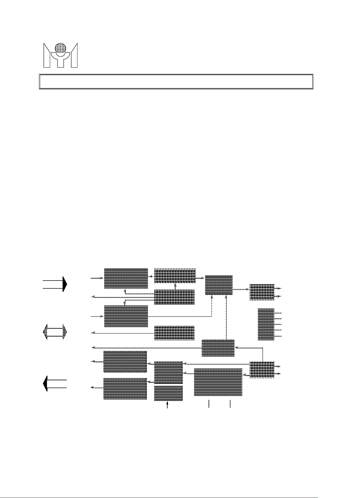
The MTD981A is a highly integrated analog interface IC for twisted pair Ethernet applications. It provides the
active circuitry to interface IEEE 802.3 media independent interface (MII) compliant controllers to 10BASE-T
or 100BASE-TX media. It also provides an ECL-type interface for use with 100BASE-FX fiber networks.
The MTD981A supports full duplex operation at 10 and 100 Mbps. Its operating condition can be set by
using Auto-Negotiation, parallel detection, or manual control. The MTD981A is ideal as a media interface for
10BASE-T/100BASE-TX network interface cards, motherboards, 10/100 repeaters, switching hubs, and
external PHYs.
BLOCK DIAGRAM
100M
Transmit
10M
MII Reg-
isters &
Interface
MII Serial
Management &
Control
Receive
Logic
Scrambler,
Parallel/Serial
Manchester
Encoder
Manchester
Parallel
NRZ/NRZI,
TX Clock
Generator
Clock
Recovery
Clock Ref-
erence
Pulse
Filter
tiation
Vcc Ground
10M
100M
UTP
Driver
LEDs
UTP
TXOP
TXON
LINK
TX
RX
100X
RXIP
RXIN
This datasheet contains new product information. Myson Technology reserves the rights to modify the product specification without
notice. No liability is assumed as a result of the use of this product. No rights under any patent accompany the sale of the product.
1/18
MTD981A Revision 1.2 02/19/2001
Page 2

MYSON
40
1 2 3 4 5 6 7 8 9 10 11 12 13 14 15 16 17 18 19 20 21 22 23 24 25 26 27 28 29 30
NC12
NC13
NC11
NC10
80 79 78 77 76 75 74 73 72 71 70 69 68 67 66 65 64 63 62 61 60 59 58 57 56 55 54 53 52 51
TECHNOLOGY
PIN CONNECTION
NC17
NC18
NC19
NC20
NC21
VAAEQ
VAAFQ
MTD981A
LEDSPD_
LEDCOL_
LEDLNK_
GNDCRV
SEL1
SEL0
VAACRV
SEL2
OGND
LEDFD_
LED10_
ANEN
LEDRX_
LEDTX_
OVDD
MDINT
CRS
COL
NC16
NC15
NC14
RPTR
SDP
RXIN
RXIP
GNDEQ
FIN
FIP
TEST2
FOP
FON
GNDREF
RBIAS
VAAREF
NC0
NC1
GNDT
TXOP
TXON
VAAT
81
82
83
84
85
86
87
88
89
90
91
92
93
94
95
96
97
98
99
100
NC2
NC3
NC4
NC5
NC6
MODE0
50
TXD3
49
TXD2
48
TXD1
47
TXD0
46
CVDD
45
CGND
44
TXEN
43
TXCLK
42
TXER
NC9
41
RXER
40
RXCLK
39
RXDV
38
OGND
37
OVDD
36
RXD0
35
RXD1
34
RXD2
33
RXD3
32
MDC
31
MTD981AF
MTD981AF
NC8
NC7
TP125
MODE1
PHYAD0
PHYAD1
PHYAD2
PHYAD3
PHYAD4
OVDD
OGND
GNDPLL
VAAPLL
PD
RST_
TEST
RMIISEL
CKIN
GNDT
ISO
ISODEF
2
MTD981A Revision 1.2 02/19/2001
Page 3

MYSON
COL
CRS
MDINT
LEDSPD_
TP125
MODE1
PHYAD0
PHYAD1
60 59 58 57 56 55 54 53 52 51 50 49 48 47 46 45 44 43 42 41
1 2 3 4 5 6 7 8 9 10 11 12 13 14 15 16 17 18 19 20
TECHNOLOGY
LEDFD_
LED10_
VAAEQ
VAAFQ
ANEN
SEL1
SEL0
VAACRV
SEL2
MTD981A
LEDCOL_
LEDLNK_
GNDCRV
OGND
LEDRX_
LEDTX_
OVDD
RPTR
SDP
RXIN
RXIP
GNDEQ
FIN
FIP
TEST2
FOP
FON
GNDREF
RBIAS
VAAREF
NC0
NC1
GNDT
TXOP
TXON
VAAT
61
62
63
64
65
66
67
68
69
70
71
72
73
74
75
76
77
78
79
80
ISODEF
MODE0
MTD981AG
RST_
TEST
RMIISEL
CKIN
GNDT
ISO
VAAPLL
PD
GNDPLL
PHYAD2
PHYAD3
PHYAD4
OVDD
OGND
40
TXD3
39
TXD2
38
TXD1
37
TXD0
36
CVDD
35
CGND
34
TXEN
33
TXCLK
32
TXER
31
RXER
30
RXCLK
29
RXDV
28
OGND
27
OVDD
26
RXD0
25
RXD1
24
RXD2
23
RXD3
22
MDC
21
3
MTD981A Revision 1.2 02/19/2001
Page 4

MYSON
Test mode select. Weakly pull down.
TECHNOLOGY
PIN DESCRIPTION
MTD981A
Name IO Pin #
TXD3 I 40 50 Transmit data bit 3.
TXD2 I 39 49 Transmit data bit 2.
TXD1 I 38 48 Transmit data bit 1.
TXD0 I 37 47 Transmit data bit 0.
TXEN I 34 44 Transmit enable.
TXCLK O 33 43 Transmit clock.
TXER I 32 42 Transmit error.
RXD3 O 23 33 Receive data bit 3.
RXD2 O 24 34 Receive data bit 2.
RXD1 O 25 35 Receive data bit 1.
RXD0 O 26 36 Receive data bit 0.
RXDV O 29 39 Receive data valid.
RXER O 31 41 Receive data error.
RXCLK O 30 40 Receive clock.
COL O 41 56 Collision detect.
CRS O 42 57 Carrier sense.
MDC I 22 32 MII management clock.
MDIO IO,U 21 31 MII management data input/output. Weakly pull up.
MDINT O 43 58 MII management interrupt.
TXOP O 77 97 Twisted-pair output positive node.
TXON O 78 98 Twisted-pair output negative node.
RXIP I 64 84 Twisted-pair input positive node.
RXIN I 63 83 Twisted-pair input negative node.
FOP O 69 89 Fiber output positive node.
FON O 70 90 Fiber output negative node.
FIP I 67 87 Fiber input positive node.
FIN I 66 86 Fiber input negative node.
SDP I 62 82 Signal detect positive node. Used only in fiber mode.
LEDSPD_ IO,U 44 59 100BT LED. 0 = 100baseTX; 1 = other connection.
LED10_ O 57 72 10BT LED. 0 = 10baseTX; 1 = other connection.
LEDTX_ O 47 62 Transmit LED. Toggles when there is transmit activities.
LEDRX_ O 46 61 Receive LED. Toggles when there is receive activities.
LEDFD_ O 58 73 Full-duplex LED. 0 = full duplex; 1 = half duplex.
LEDLNK_ O 48 63 Link LED. 0 = link on; 1 = link off.
(80)
Pin #
Description
(100)
When RST_ is low, this pin works as FIBER_DESEL to select the
fiber mode. Weakly pull up
LEDCOL_ IO,U 45 60 Collision led. 0 = collision; 1 = no collision. Weakly pull up.
When RST_ is low, this pin will load the SCRAM_SEL to
enable/disable the scrambler and descrambler set.
TEST I,D 7 12
CKIN I 5 10 Oscillator input.
If RMII is selected, only 50MHz oscillator can be used. In MII
mode, a 25MHz oscillator can be used.
RBIAS I 72 92 Bias control resister, to provide the internal voltage control.
PD I,D 9 14 Power down control.
1 = power down mode; 0 or floating = normal. Weakly pull down.
RPTR I,D 61 81 Repeater mode select.
4
MTD981A Revision 1.2 02/19/2001
Page 5
MYSON
; 0 or floating = normal. Weakly pull down.
disabled. Weakly pull up.
select, bit 1. Weakly pull up.
select, bit 0. Weakly pull up.
mode select bit 0. Weakly pull down.
MTD981A
TECHNOLOGY
1 = repeater mode
ISODEF I,D 2 7 Isolate Default
1 =isolation; 0 or floating = normal. Weakly pull down.
ISO I,D 3 8 Isolate
1 =isolation; 0 or floating = normal. Weakly pull down.
RST_ I,U 8 13 Pin Reset select.
0=reset; 1or floating = normal. Weakly pull up
RMIISEL I,D 6 11 RMII mode select.
1 = RMII mode; 0 or floating = normal (MII mode).
Weakly pull down.
When RMII mode is selected, MTD981A will assume the 50MHz
oscillator is used as base clock.
ANEN I,U 56 71 Auto-Negotiation enable
1 = enable Auto-Negotiation; 0 = disable Auto-Negotiation.
Weakly pull up.
SEL2 I,U 53 68 Operation mode select, bit 2. Used only when autonegotiation is
SEL2 SEL1 SEL0 operation mode
X 0 0 mode select by MII registers
0 0 1 10BaseT, half duplex
0 1 X 100BaseT, half duplex
1 0 1 10BaseT, full duplex
1 1 X 100BaseT, full duplex
SEL1 I,U 54 69 Operation mode
SEL0 I,U 55 70 Operation mode
PHYAD0 I,U 18 23 PHY Address bit 0. Weakly pull up.
PHYAD1 I,U 17 22 PHY Address bit 1. Weakly pull up.
PHYAD2 I,U 16 21 PHY Address bit 2. Weakly pull up.
PHYAD3 I,U 15 20 PHY Address bit 3. Weakly pull up.
PHYAD4 I,U 14 19 PHY Address bit 4. Weakly pull up.
TP125 IO,D 20 25 Value latched in while reset to select transformer turns ratio.
=1 to select the transmit transformer with ratio 1.25:1
=0 to select the transmit transformer with ratio 1:1 (default)
Works as link_established after reset.
Weakly pull down.
MODE1 I,D 19 24 Test mode select bit 1. Weakly pull down.
MODE0 I,D 1 6 Test
TEST2 O 68 88 Used as the test mode output monitor pin
NC0 74 94 No Connection
NC1 75 95 No Connection
NC2 - 1
NC3 - 2
NC4 - 3
NC5 - 4
NC6 - 5
NC7 - 26
NC8 - 27
NC9 - 28
NC10 - 29
NC11 - 30
NC12 - 51
NC13 - 52
NC14 - 53
NC15
- 54
5
MTD981A Revision 1.2 02/19/2001
Page 6

MYSON
TECHNOLOGY
NC16 - 55
NC17 - 76
NC18 - 77
NC19 - 78
NC20 - 79
NC21 - 80
CVDD IO 36 46 Power pin for core.
CGND IO 35 45 Power pin for core.
MTD981A
6
MTD981A Revision 1.2 02/19/2001
Page 7

MYSON
Figure 1. MII Read/Write operation
MTD981A
TECHNOLOGY
FUNCTIONAL DESCRIPTIONS
1. Media Independent Interface (MII)
The MTD981A implements an IEEE 802.3u Clause 22 compliant MII interface described as follows. The
interface signals can be grouped into transmit, receive, and status. The transmit data signals comprise
TXD[3:0], TXEN, TXER, and TXCLK. TXD[3:0] are the nibble size data path, TXEN signals the presence of
data on TXD[3:0], TXER indicates substitution of data with the HALT symbol, and TXCLK carries the
transmit clock that synchronizes all the transmit signals. The receive data signals also include seven signals,
RXD[3:0], RXDV, RXER, and RXCLK. RXD[3:0] are the nibble size data path, RXDV signals the presence
of data on RXD[3:0], RXER indicates the validity of data, and RXCLK carries the receive clock. Depending
on the operation mode, RXCLK signal is generated by the clock recovery module of either the 100Base-X or
10Base-T receiver. Two status signals, COL and CRS, are generated in the MTD981A to indicate Collison
status and Carrier Sense status to the MAC.
2. Serial Management Interface (SMI)
The MTD981A implements a Serial Management Interface (SMI) used both to obtain status from and to
configure the PHY. This mechanism corresponds to the MII Spec for 100BASE-X (Clause 22). The SMI
interface consists of two signals, MDC and MDIO. MDC is a clock input to the PHY and is used to latch data
and instructions for the PHY. The clock rate can run up to 2.5MHz. MDIO is bi-directional and is used to
write instruction to, write data to, or read data from PHY. Each data bit is latched either in or out on the
rising edge of MDC. MDC/MDIO are a common signal pair to up to 32 PHYs. Therefore, each PHY needs
its unique address. The MTD981A uses 5 bits as PHY address. The address is latched into internal register
during reset from the pin setting. The SMI interface supports registers 0 through 6. Additional “vendorspecific” registers are implemented. All the registers are described in the register section. The access
method of these registers is described as follows.
MDC
MIDIO
(STA)
MDIO
(PHY)
MDC
MIDIO
(STA)
z
0 1 1 0 0 1 1 0 0 0 0 0 0 z 1 0 0 1 1 0 0 0 1 0 0 0 0 0 0 0 0 0
start opcode phyaddr regaddr TA register data
idle
z
0 1 0 1 0 1 1 0 0 0 0 0
start opcode phyaddr regaddr
idle
z
z
Typical MII Read Operation
0 1 0 0 0 0 0 0 0 0 0 0
0 0 0 0 0 0 0 0
TA register data
Typical MII Write Operation
7
MTD981A Revision 1.2 02/19/2001
z
zz
idle
z
z
idle
Page 8

MYSON
MTD981A
TECHNOLOGY
Before any transaction, the station must send 32 continuous logic "1" on MDIO to establish synchronization.
Figure 1 shows the read and write operation. The start code is "01" followed by an op code, either "01" for
read or "10" for write. For read operation, the device address must match the address of the target PHY
device. For write operation, the address may be all zero or match a specific PHY address. Turnaround cycle
is an idle cycle consists of two bit times between the register address field and data field in order to avoid
conflict. For reading, no device drive MDIO in the first bit time, PHY drive "0" in the second bit time. For
writing, station drive "10" during the idle cycle.
3. 10BASE-T
When configured to run in 10BASE-T mode, either through hardware configuration, software, or AutoNegotiation, the MTD981A will support all the functions specified in IEEE 802.3 Standard for 10BASE-T
(Clause 14).
3.1 Transmit Function
In 10BASE-T mode, the transmit function uses parallel-to-serial logic to convert the 4-bit transmit data into a
serial data stream. This serial data stream is Manchester-encoded and then output through the
waveshaping driver. Filtering is performed in silicon to reduce EMI emission. TXOP/TXON can be
connected directly to a standard transformer. External filtering modules are not needed
3.2 Receive Function
In 10BASE-T mode, the signals at RXIP/RXIN first pass a smart squelch circuit. A Manchester decoder and
a serial-to-parallel converter then follow to generate the 4-bit nibble in MII interface. The squelch level of the
smart squelch circuit drops to half its threshold value after unsquelch to allow reception of minimum
amplitude signals to mitigate carrier fade in the event of worst case signal attenuation.
3.3 Link Monitor
In 10BASE-T mode, link pulse detection circuit will constantly monitor the RXIP/RXIN pins for the presence
of valid link pulses. In the absence of valid link pulses, the LINK led will deassert.
4. 100BASE-TX
When configured to run in 100BASE-T mode, either through hardware configuration, software, or AutoNegotiation, the MTD981A will support all the functions specified in IEEE 802.3 Standard for 10BASE-TX.
4.1 Transmit Function
In 100BASE-TX mode, the transmit function converts synchronous 4-bit data nibbles from the MII to a 125Mbps differential serial data stream in MLT-3 format. The entire operation is synchronous to a 25-MHz clock
and a 125-MHz clock. Both clocks are generated by an on-chip PLL clock synthesizer that is locked to an
external 25-MHz clock source. There are three functional blocks in the transmit function: 4B/5B encoder,
scrambler, and MLT-3 output driver. The 4B/5B encoder, defined in IEEE 802.3 Clause 24, converts 4-bit
raw data to 5-bit code-group. It also inserts the stream boundary delimiters (/J/K/ and /T/R/) at the beginning
and end of the data stream as appropriate. The 4B/5B encoded data has repetitive patterns which result in
peaks in the RF spectrum. The peaks in the radiated signal are reduced significantly by scrambling the
transmitted signal. The scrambler, defined by the TP-PMD Stream Cipher function, encodes a plain text
NRZ bit stream using a key stream periodic sequence of 2047 bits generated by the recursive linear function:
X[n] = X[n-11] + X[n-9] (modulo 2)
The scrambler reduces peak emission by randomly spreading the signal energy over the transmit frequency
range, thus eliminating peaks at a single frequency. The scrambled NRZ data stream is then converted to
MLT-3 encoded data and then output to the UTP-5 cable. The MLT-3 is a tri-level signal. The presence of a
transition has a logical value of 1 and the lack of a transition has a logical value of 0. The benefit of MLT-3 is
that it reduces the the maximum frequency from 62.5 MHz to 31.25 MHz.
8
MTD981A Revision 1.2 02/19/2001
Page 9

MYSON
When configured to run in 100BASE-FX mode, either through hardware configuration or software
SEL[0:2]. MTD981A also implements parallel detect function to allow compatibility with legacy
MTD981A
TECHNOLOGY
4.2 Receive Function
In 100BASE-TX mode, the receive function includes a receiver with adaptive equalization and baseline
wander compensation, data and clock recovery at 125MHz, descrambling, and 5B to 4B decoding. An
energy detect circuit is also added to determine whether there is any signal energy on the media.
4.3 Link Monitor
In 100BASE-TX mode, when no signal or invalid signal is detected on the receiver pair, the link monitor will
enter the “link fail” state where only the scrambled idle code will be transmitted. When a valid signal is
detected for a minimum period of time, the link monitor will then enter the “link pass” state when transmit and
receive functions are entered.
5. 100BASE-FX
configuration, the MTD981A will support all the features and parameters of the industry standards.
5.1 Transmit Function
In 100BASE-FX mode, the 4B/5B encoded data stream bypass the scrambler. The output is NRZI PECL
signals. The PECL level signals are used to drive the transmitter of the fiber module.
5.2 Receive Function
In 100BASE-FX mode, the signal is received through the PECL receiver, and directly passed to the clock
recovery circuit for clock/data extraction. The descrambler is bypassed. The data still need 5B/4B decoding.
5.3 Link Monitor
In 100BASE-FX mode, the external fiber module performs the signal energy detection and communicates this
information directly to the SDP pin of MTD981A.
6. Auto-Negotiation
MTD981A implements Auto-Negotiation logic conforming to the 802.3u specification. The basic operation is based on
using Fast Link Pulse (FLP) to communicate information between link partners. The Auto-Negotiation takes three
phases to complete: advertising, detection and selection. The Auto-Negotiation mode can be optionally selected using
external pin selection
network devices.
9
MTD981A Revision 1.2 02/19/2001
Page 10

MYSON
TECHNOLOGY
REGISTER DESCRIPTIONS
Register 0. Control Register
Bit Name R/W Def Description
15 RST RW,SC0 Reset
1 = reset.
0 = Normal operation.
14 LPBK RW 0 Loopback select.
1 = Loopback
0 = Normal operation.
13 SPEED RW 1 Speed select.
1 = 100Mbps selected.
0 = 10Mbps selected.
12 ANEN RW 1 Autonegotiation enable.
1 = Enabled.
0 = Disabled.
11 PWDN RW 0 Power down enable.
1 = Power down.
0 = Normal operation.
10 ISO RW 1 MII isolation.
1 = Isolation.
0 = Normal operation.
9 RESTART_ANRW,SC0 Restart autonegotiation.
1 = Restart.
0 = Normal operation.
8 DUPLEX RW 0 Duplex mode select.
1 = Full Duplex.
0 = Half Duplex.
7 COLTST RW 0 Collision test enable.
1 = Enable.
0 = Disable.
6:0 - - - reserve
MTD981A
Register 1. Status Register
Bit Name R/W Def Description
15 T4 R 0 Not capable of T4 operation.
14 TXFD R 1 Capable of 100-TX full duplex operation.
13 TXHD R 1 Capable of 100-TX half duplex operation.
12 TPFD R 1 Capable of 10-TP full duplex operation.
11 TPHD R 1 Capable of 10-TP half duplex operation.
10:7 - - - Reserved.
6 SPREM R 1 Accepting MII frames with preamble suppressed.
5 ANC R 0 1 = Auto-Negotiation complete.
0 = Auto-Negotiation not complete.
4 RF R,LH 0 1 = Remote fault detected.
0 = No remote fault.
3 AN R 1 1 = Capable of Auto-Negotiation operation.
2 LINK R/LL 0 1 = Link established.
0 = Link not established.
1 JAB R/LH 0 1 = Jabber detected.
0 = Jabber not detected.
0 EXT R 1 1 = Extended registers exist.
10
MTD981A Revision 1.2 02/19/2001
Page 11

MYSON
TECHNOLOGY
Register 2. OUI Register
Bit Name R/W Def Description
15:0 OUI_L R 0302hOUI[3:18] = 0302h
Register 3. OUI_H Register
Bit Name R/W Def Description
15:10 OUI_H R 1101
9:4 PARTNO R 0 Part number.
3:0 REV R 0 Revision number.
Register 4. Advertisement Register
Bit Name R/W Def Description
15 NP R 0 Next Page.
14 ACK R 0 Acknowledge.
13 RFDET R 0 Remote fault detected.
12:10 - RW 000 Reserved. ( reserved for pause function )
9 T4 R 0 1 = Capable of T4 operation.
8 TXFD RW 1 1 = Capable of 100-TX full duplex operation.
7 TXHD RW 1 1 = Capable of 100-TX half duplex operation.
6 TPFD RW 1 1 = Capable of 10-TP full duplex operation.
5 TPHD RW 1 1 = Capable of 10-TP half duplex operation.
4:0 SELECT R 1 Selector field = 5’b00001 means IEEE802.3 selected.
OUI[19:24] = 1101_00
_00
0 = No next page.
1 = Received link code word acknowledged.
0 = Received link code word not acknowledged.
1 = Remote fault detected.
0 = No remote fault.
0 = Not capable of T4 operation.
0 = Not capable of 100-TX full duplex operation.
0 = Not capable of 100-TX half duplex operation.
0 = Not capable of 10-TP full duplex operation.
0 = Not capable of 10-TP half duplex operation.
MTD981A
Register 5. Link Partner Ability Register
Bit Name R/W Def Description
15 NP R 0 Next Page.
0 = No next page.
14 ACK R 0 Acknowledge.
1 = Received link code word acknowledged.
0 = Received link code word not acknowledged.
13 RFDET R 0 Remote fault detected.
1 = Remote fault detected.
0 = No remote fault.
12:10 - R - Reserved.
9 T4 R 0 1 = Capable of T4 operation.
0 = Not capable of T4 operation.
8 TXFD R 0 1 = Capable of 100-TX full duplex operation.
0 = Not capable of 100-TX full duplex operation.
7 TXHD R 0 1 = Capable of 100-TX half duplex operation.
11
MTD981A Revision 1.2 02/19/2001
Page 12

MYSON
TECHNOLOGY
0 = Not capable of 100-TX half duplex operation.
6 TPFD R 0 1 = Capable of 10-TP full duplex operation.
0 = Not capable of 10-TP full duplex operation.
5 TPHD R 0 1 = Capable of 10-TP half duplex operation.
0 = Not capable of 10-TP half duplex operation.
5 TPHD R 0 1 = Capable of 10-TP half duplex operation.
0 = Not capable of 10-TP half duplex operation.
4:0 SELECT R 1 Selector field = 5’b00001 means IEEE802.3 selected.
Register 16. Proprietary Control Register
Bit Name R/W Def Description
15 REP RW 1 = Repeater mode.
- full duplex disabled.
- SQE function disabled.
- CRS response to receive activity only.
14 INT_SEL RW 0 1 = set the interrupt pin to be active high.
0 = set the interrupt pin to be active low.
13:12 stable_time_
sel[1:0]
11 SQE_DIS RW 0 1 = Disable SQE function.
10 FLP_RX_
IDLE_EN
9 FDDI_
LOAD_EN
8 EDPSM RW 0 1 = energy detect power saving mode
7 FEF_EN RW 0 1 = Far-End-Fault enabled.
6 XFSEL RW 0 1 = Select transmit transformer ratio to be 1.25:1.
5 POL_DIS RW 0 1 = Disable auto polarity detection/correction function.
4 NLP_DIS RW 0 1 = Force link up without checking NLP.
3 - - - Reserved.
2 BP_JAB RW 0 1 = Bypass jabber function.
SCRAM_EN
1
0 FX_SEL RW 0 1 = FX mode selected, SCRAM_EN will be set to 0.
RW 00 Stablize timer sel
00 = 700us
01 = 1ms
10 = 5ms
11 = 45ms
0 = Enable SQE function.
RW 1 FLP_idle enable (arbitration state machine)
1 single_link_ready = (flp_idle) &
(( (link_status_nlp == 1'b0) & (link_status_x == READY)) |
( (link_status_nlp == 1'b1) & (link_status_x != READY)) );
0 single_link_ready =
(( (link_status_nlp == 1'b0) & (link_status_x == READY)) |
( (link_status_nlp == 1'b1) & (link_status_x != READY)) );
RW 1 FDDI load enable (descrambler lock time)
1 load = (~locked) & ( quiet | halt | master | idle);
0 load = (~locked) & ( idle);
0 = no power down
0 = Far-End-Fault disabled.
0 = Select transmit transformer ratio to be 1:1.
0 = Enable auto polarity detection/correction function.
0 = Normal operation.
0 = Enable jabber function.
RW 1 1 = Enable scrambler / discrambler
0 = Disable scrambler / discrambler
0 = Disable FX mode. SCRAM_EN can be programmed after FX
mode disabled.
MTD981A
12
MTD981A Revision 1.2 02/19/2001
Page 13

MYSON
TECHNOLOGY
Register 17. Interrupt Register
Bit Name R/W Def Description
15:13 - - - Reserved.
12 PDFM RW 0 1 = Enable parallel detection fault interrupt.
0 = Disable parallel detection fault interrupt.
11 - - - Reserved.
10 LFM RW 0 1 = Enable link fail interrupt.
0 = Disable link fail interrupt.
9 - - - Reserved.
8 ANCM RW 0 1 = Enable autonegotiation complete interrupt.
0 = Disable autonegotiation complete interrupt.
7:5 - - - Reserved.
4 PDFINT W1C 0 1 = Parallel detection fault interrupt.
This bit is write 1 cleared.
3 - - - Reserved.
2 LFINT W1C 0 1 = Link fail interrupt.
This bit is write 1 cleared.
1 - - - Reserved.
0 ANCINT W1C 0 1 = Autonegotiation complete interrupt.
This bit is write 1 cleared.
MTD981A
Register 18. Proprietary Status Register
Bit Name R/W Def Description
15:12 - - - Reserved.
11 DUPLEX R 0 1 = link status is full duplex.
0 = link status is half duplex or link fail.
10 SPEED R 0 1 = link speed is 100Base-TX.
0 = link speed is 10Base-TX.
9:5 - - - Reserved.
4:0 PHYAD R
Register 19. Test Register
Bit Name R/W Def Description
15:14 TSTMD[3:2]RW 00 125mHz clock source
13:12 TSTMD[1:0]RW 00 mlt3shmx control signal.
11:8 RESERVEDRW 0 Reserved
NO_PWRDN
7
MANUAL_CT
6
RL_PWRDN
5:4 RESERVEDRW 0 Reserved
00000
PHY Address.
00 = use internal(cgm) 125MHz clk
11 = use external 125MHz clk
00 = clk0 clkd0 nrz0 è (normal mode)
01 = clk0 clkd0 (high) è (test mode with nrz high and clk from
cgm)
10 = f25m f25m (high) è(test mode with nrz high and clk from
ckin)
11 = f25m f25m (high) è(test mode with nrz high and clk from
ckin)
RW 0 1 = Force no power down.
0 = Accept power down setting.
RW 0 1 = Enable manual control power down.
0 = Bypass manual control power down.
3 TSTMD_
DESCRM
RW 0 1 = Accelerate descrambler lock time.
0 = Normal descrambler lock time.
13
MTD981A Revision 1.2 02/19/2001
Page 14

MYSON
TECHNOLOGY
2 LB_DIG RW 1 1 = Enable digital loopback.
0 = Disable digital loopback.
1:0 RESERVE
D
Reserved
MTD981A
14
MTD981A Revision 1.2 02/19/2001
Page 15

MYSON
MTD981A
TECHNOLOGY
ELECTRICAL CHARACTERISTICS
1. Absolute Maximum Ratings
at: Ta= 0 to 70 oC, VSS=0V
Name Symbol Range Unit
Maximum Supply Voltage VDD -0.3 to +5.0 V
Maximum Input Voltage Vin -0.3 to VDD+0.3 V
Maximum Output Voltage Vout -0.3 to VDD+0.3 V
Maximum Storage Temperature Tstg -25 to +125 o
2. Operating Range
Name Symbol Min. Max. Unit
Supply Voltage VDD 3.0 3.6 V
Operating Temperature Topg 0 +70
oC
C
15
MTD981A Revision 1.2 02/19/2001
Page 16

MYSON
TECHNOLOGY
PACKAGE DIMENSION
100-pin PQFP
MTD981A
0.063
0.031 +/-0.006
0.551 +/-0.004
0.677 +/-0.008
0.787 +/-0.004
0.913 +/-0.008
0.014 +/-0.004
0.012 +/-0.0040.026
0
0~7
0.006 +/-0.002
0.107 +/-0.006
16
MTD981A Revision 1.2 02/19/2001
Page 17

80-pin LQFP
0.0079~0.0157
0.0256
0.063 Max.
0.002~0.006
0.055 +/-0.002
0.00.9 Ref.
MYSON
TECHNOLOGY
0.47 2 BSC.
0.55 1 BSC.
MTD981A
0.472 BSC.
0.551 BSC.
12o +/-1
o
17
MTD981A Revision 1.2 02/19/2001
Page 18

MYSON
MTD981A(Preliminary) -> MTD981A
TECHNOLOGY
DOCUMENT CHANGE HISTORY
Revision Chapter Detail
1.1 Document Change
History
Product name of 80pin LQFP
Pin Description
RBIAS_RET
Pin Diagram RBIAS_RET -> NC0
Pin Description of
PA4 – PA0
Pin Description of
TPOP/TPON
Pin Description of
TPIP/TPIN
Pin Description of
RMIISEL
Pin Description of
ANEN
Pin Description of
ISO
Pin Description of
ISODEF
Pin Description of
TEST2
Pin Description of
LEDCOL_
Pin Description of
LEDLNK_
1.2 Pin Diagram GNDEQ -> NC21
Pin Description Add NC21 description
Add this new Chapter
MTD981A -> MTD981AG
Rename as NC0
Rename as PHYAD4-0 (consistent with Pin Diagram)
Phy ID -> PHY Address
Rename as TXOP/TXON (consistent with Pin Diagram)
Rename as RXIP/RXIN (consistent with Pin Diagram)
My3045 -> MTD981A
50M -> 50MHz
autonegotiation -> Auto-Negotiation
isolation select -> Isolate
isolation select -> Isolate Default
I ->O; vcp -> test mode output monitor pin
Add scram_sel description
Remove scram_sel description
MTD981A
Revision number and date
18
MTD981A Revision 1.2 02/19/2001
 Loading...