

Page 1
ut notice.
No liability is assumed as a result of the use of this procuts. No rights under any patent accompany the sales of the product.
MYSON
GENERAL DESCRIPTION
Supports both full-duplex and half-duplex mode
duplex flow control method.
Contains separate transmit and receive FIFOs.
Supports Magic packet and Microsoft wake-up
frame filtering.
Supports ACPI and PCI power management.
Supports up to 128K bytes boot ROM or flash
memory without external latch.
Programmable EEPROM interface.
perform ACPI function, and the capability of sensing
PME# WakeUp
TXD[3:0]
MTD 800
TECHNOLOGY
Integrated Fast Ethernet Controller
FEATURES
• Compliant to PCI bus interface v2.2.
• IEEE802.3 and 802.3u compliant.
• High performance with PCI bus master structure.
• Programmable PCI burst length for low CPU utilization rate.
• Transmit packet queuing capability for higher performance.
•
operation.
• Supports both IEEE802.3x and XON/XOFF full
•
•
•
• Supports CardBus STSCHG pin and status
changed registers. The CIS can be stored in the
EEPROM.
•
(Preliminary)
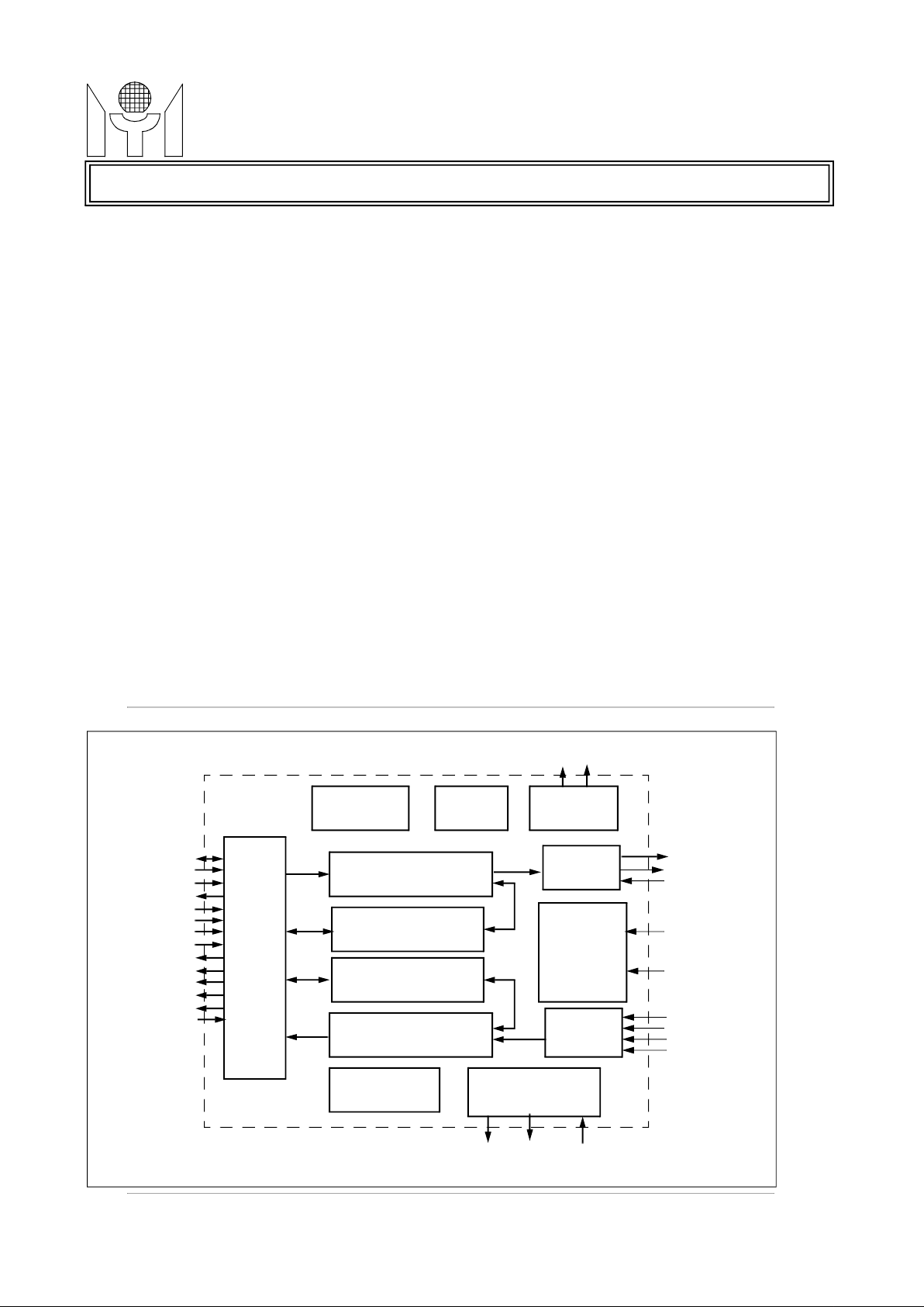
MTD800 is a highly integrated fast ethernet
controller for PCI interface. The chip contains a PCI
interface block, two large FIFOs( each is 2KiloBytes )
for transmit and receive DMA, IEEE802.3 and 802.3u
compliant MAC interface for MII connection. Besides
that, the chip has the built-in Wake-Up controller to
IEEE 802.3x frame to support XON/XOFF flow control protocol. The chip also has EEPROM and BootROM interface for no glue logic board
implementation. For CardBus application, MTD800
supports four status-changed registers, an interface
for accessing CIS which is stored in EEPROM and
STSCHG pin to reflect the general wake-up event.
• Autoload EEPROM contents after power-on.
•
• 128 pin PQFP package.
• Single 3.3V Power Supply.
BL OCK DIAGRAM
EEPROM
Control Logic
AD[31:0]
PCICLK
RST#
INTA#
CBE3[3:0]
IDSEL
FRAME#
IRDY#
TRDY#
DEVSEL#
STOP#
PAR
REQ#
GNT#
PCI
Interface
Tx FIFO
Tx DMA Control
Rx DMA Control
Rx FIFO
Boot ROM
Interface
LED
LED Control
Tx MII
Interface
MAC
Protocol
Processor
Rx MII
Interface
TXEN
TXCK
CRS
COL
RXD[3:0]
RXDV
RXCK
RXER
CFG & CSR
Registers
This datasheet contains new product information. Myson Technology reserves the rights to modify the product specification witho
1/42 MTD800 Revision 0.0 07/20/1999
Wake-up
Controller
IOSLATE#
Page 2

MYSON
PCICLK provides timing reference for the MTD800 related PCI transac-
drain pins are floated. This signal is asynchronous to PCICLK and have to
be asserted for at least 10 active PCI clock cycles.
address phase followed by one or more data phases. During the first cycle
while it is considered as a data bus during subsequent cycles.
BRWR#
WUP/SGH
MTD 800
TECHNOLOGY
1.0 PIN CONNECTION
128 pin QFP
VDD_M
MDIO
MDC
102
101
VSS_M
COL
CRS
RXER
RXD3
RXD2
RXD1
RXD0
RXCK
VDD
VSS
TXEN
TXD3
TXD2
TXD1
TXD0
TXCK
RXDV
INTA#
RST#
VDD
PCICLK
VSS
GNT#
REQ#
PME#
103
104
105
106
107
108
109
110
111
112
113
114
115
116
117
118
119
120
121
122
123
124
125
126
127
128
100
010203040506070809
(Preliminary)
PAUSE
ACT
EpSel
ByPass#
VSS
VDD
VDD
RSTOUT#
ISOLATE#
VSS
BRA16
BRA15
BRA14
BRA13
BRA12
BRA11
BRA10
BRA9
BRA8
BRA7
VSS
VDD
BRA6
BRA5
BRA4
BRA3
BRA2
BRA1
BRA0
BRD7
BRD6
VSS_M
VDD_M
BRD5
9998979695949392919089888786858483828180797877767574737271706968676665
MTD800
1011121314151617181920212223242526272829303132333435363738
BRD4
64
TEST#
63
BRD3
62
BRD2
61
BRD1
60
BRD0
59
BRCS#
58
BRRD#
57
ECS
56
VSS
55
VDD
54
53
AD0
52
AD1
51
AD2
50
AD3
49
AD4
48
AD5
47
AD6
46
AD7
45
CBE0#
44
AD8
43
AD9
42
AD10
41
VDD
40
VSS
39
VSS
AD31
AD30
AD29
VDD
AD28
AD27
AD26
AD25
AD24
AD23
AD22
IDSEL
CEB3#
VSS
VSS
VDD
VDD
AD21
AD20
AD19
AD18
AD17
2.0 PIN DESCRIPTIONS
Name Pin # I/O Description s
PCI Bus Interface
PCICLK 124 I
RST# 122 I
1 - 6,
9, 10
13 -15
AD[31:0]
20 - 24,
34 - 38,
41 - 43,
45 -52
tions. All PCI signals except RST#,INTA# and PME# are sampled on the
rising edge of this clock.
When RST# is asserted, all output signals are put into tristate and all open
32-bit multiplexed address and data bus. A bus transaction consists of an
I/O
in which the FRAME# is asserted, the AD[31:0] represents the address bus
AD16
IRDY#
CBE2#
TRDY#
FRAME#
PAR
AD15
CBE1#
STOP#
PERR#
DEVSEL#
AD11
AD14
AD13
AD12
2/42 MTD800 Revision 0.0 07/20/1999
Page 3

MYSON
4-bit multiplexed bus command and byte enables. During the address
cycles, CBE represents the byte enable signals for PCI data bus.
this signal is asserted to indicate that the master is ready to accept data
from the selected target. Wait states are inserted until both IRDY# and
TRDY# are asserted.
used in conjunction with IRDY#. A data phase is completed on any clock
when both IRDY# and TRDY# are asserted.
Asserted by MTD800 to indicate that the device has decoded the address
DEVSEL# indicates whether any device on the bus or bridge has termi-
INTA# is an asynchronous signal which is used to request an interrupt.
Asserted by the PCI bus arbiter to indicate that MTD800 has granted the
Asserted by MTD800 to signal bus arbiter that it needs the dedicated
by MTD800 to request a change in the device or system power state.
Collision signal. COL is asserted high when PHY detects a collision on the
Transmit Data signals. TXD are driven by MTD800 and transits synchro-
nously with respect to the TXCK.
Transmit Data Enable. TXEN is driven by MTD800 and transits synchro-
nously with respect to the TXCK.
MTD 800
TECHNOLOGY
Name Pin # I/O Description s
CBE#[3:0]
IDSEL 12 I Used as a chip select during access to the configuratio n registers
FRAME# 26 I/O
IRDY# 27 I/O
TRDY# 28 I/O
DEVSEL# 29 I/O
STOP# 30 I/O
INTA# 121 O/D
PAR 32 I/O
1 1, 25,
33, 44
I/O
phase transaction, CBE is considered as bus command. On the data phase
Driven by MTD800 to Indicate the start and duration of a transaction. The
FRAME# is deasserted when the master is ready to complete the final data
phase in the transaction.
During a write transaction, the current bus master asserts IRDY# to indicate
that valid data is being driven onto the PCI bus. During a read transaction,
During a read transaction, the target asserts TRDY# to indicate that valid
data is being driven onto the PCI bus. During a write transaction, this signal
is asserted to indicate that the target is ready to accept data. TRDY# is
as the target of current access. As an input, DEVSEL# indicates whether
any device on the bus has been selected.
Asserted by MTD800 to disconnect any further transaction. As an input,
nated the transaction.
Ensures even parity across AD[31:0] and CBE[3:0]. PAR is stable and valid
for one clock after the address phase. During the data phase, PAR is stable
and valid for one clock after either IRDY#(write transaction) or TRDY#(read
transaction) is asserted.
(Preliminary)
GNT# 126 I
REQ# 127 O/Z
PERR# 31 I/O PERR# is asserted when a data parity error is detected.
PME# 128 O/D
COL 104 I
RXDV 120 I
TXCK 119 I
TXD[3:0]
TXEN 114 O
RXCK 11 1 I
115 118
bus control authority.
access to the PCI bus.
An interrupt signal for the occurrence power management event. Asserted
Netwo r k Interface
medium. This signal is asynchronous to TXCK or RXCK.
Receive data valid. RXDV is asserted high by PHY to indicate the incoming
receive data RXD[3:0] is valid. This signal is synchronous to RXCK.
Transmit Clock. TXCK is a continuous clock that provides the timing refer-
ence for the transfer of the TXD[3:0] and TXEN signals.
O
Receive Clock. RXCK is a continuous clock that provides the timing reference for the transfer of the RXD[3:0], RXDV and RXER.
3/42 MTD800 Revision 0.0 07/20/1999
Page 4

MYSON
Carrier Sense signal. CRS is asserted by PHY when either the transmit or
receive medium is non-idle. This signal is asynchronous to TXCK or RXCK.
Management Data Clock. MDC is sourced by the MTD800 to control the
to PHY. A 1.5K pull up resistor is required to connect to this pin.
MII interface. A 510 ohm pull up resistor is required to connect to this pin.
BootROM read signal. Read out the content of BootROM onto the memory
BootROM write signal. When flash memory is used, BRWR# is asserted
A chip select signal for the external EPRO M (BootROM) or flash memory.
A multiplexed signal for BootROM data bit 0 and Serial ROM Data input.
A multiplexed signal for BootROM data bit 1 and Serial ROM Data output.
BootROM data bus from bit 3 to bit 7.
BootROM address bus from bit 0 to bit 16.
Misc. Interface
Wakeup Pin/CardBus STSCHG Pin.
In PCI application, this pin is the Wakeup pin to signal the host system of an
wakeup event happened.
EEPROM Bypass Mode. When asserted low, the EEPROM function will be dis-
MTD 800
TECHNOLOGY
Name Pin # I/O Description s
RXD[3:0]
RXER 106 I
CRS 105 I
MDC 100 O
MDIO 101 I/O
LED_ACT# 98 O
LED_PAUS
E#
ECS 56 O
107 110
99 O
Receive Data signals. RXD are driven by PHY and transit synchronously
I
with respect to the RXCK.
Receive Error signal. RXER is asserted high to indicate a coding error is
detected by PHY. This signal is synchronous to RXCK.
transfer of the MDIO data. A 1.5K pull up resistor is required to connect to
this pin.
Management Data Input/Output. A bi-directional data interface connected
LED Status Output
Activity LED. This signal will drive the led light on when detecting activity on
Pause LED. This signal will drive the led light on when detecting transmission is paused under the condition of receiving a XON frame.
Bo o tROM/ EEPROM Int er face
A chip select signal for the external EEPROM. EEPROM is used to provide
the configuration data and Ethernet Address. A 100K pull-up resister is connected to this pin.
(Preliminary)
BRRD# 57 O
BRWR# 58 O
BRCS# 59 O
BRD0/EEDI 60 I/O
BRD1/EEDO 61 I/O
BRD2/EECK 62 I/O A multiplexed signal for BootROM data bit 2 and Serial ROM Clock signal.
70 - 69,
BRD[7:3]
BRA[16:0]
WAKEUP/
STSCHG
66 - 65, 63I/O
89- 80,
77 - 71
53 O/Z
support data bus.
low to enable the write action.
The BootROM contains codes that can be usually executed for a system
boot function.
O
In Card bus application, this pin is used as the STSCHG pin to signal the system of
any status changed. This pin is enabled as STSCHG pin if the PME_Enable bit of
the power management control register is set and the FMR.GWAKE, FMR.WAKE
are both set.
ByPass# 96 I
able. This is useful for testing purpose. For normal operation, it should be connected to VDD.
4/42 MTD800 Revision 0.0 07/20/1999
Page 5

MYSON
ISOLATION pin. This pin should connect to the PCI stable power signal
(VDD). When PCI Bus is in B3 state, the power signal becomes deas-
serted, however the ISOLATION pin is active. Under this condition, the
PME# are isolated from the PCI Bus.
Hardware reset is detected. The pulse width is 245us. The PHY can use
this output pin as its reset signal, then PHY can avoid to keep being reset
MTD 800
TECHNOLOGY
Name Pin # I/O Description s
EEPROM selection pin. EpSel is to determine which type of EEPROM is
EpSel 97 I
ISOLATE# 91 I
RSTOUT# 92 O
VDD_M,
VSS_M
VDD
VSS
67, 102
68, 103
7, 16,
17, 40,
54,64,
78, 93,
94,
112,
123
8, 18,
19, 39,
55, 79,
90, 95,
113,
125
chosen. 93C46 is used when EpSel connects to VSS, while 93C66 is
selected if EpSel connects to VDD.
PCIRST# and PCICLK are ignored and all the PCI output signals except
Reset Output pin. A active-low pulse is generated when Power-On or
during D3 state.
Power Supply & Ground
P/G Digital 3.3V power and ground for internal SRAM.
P Digital 3.3V power supply.
G Digital Ground.
(Preliminary)
5/42 MTD800 Revision 0.0 07/20/1999
Page 6

MYSON
3.0 FUNCTIONAL DESCRIPTION
putation. The MTD800 is directly compatible with revision 2.2 of the PCI Local Bus Specification and supports
with the host memory.
The DMA Transmit Function is responsible for fetching data from the host’s memory into the on-chip transmit
FIFO, and then signalling MAC transmit interface to relay the transmitted data onto the network if the fullness
buffers. The transmit descriptor format is shown as figure 3.2. It consists of four long words. The first two
words contain the transmit frame status, frame length and the descriptor ownership information. The last two
descriptor words are given in table 3.1 and table 3.2 respectively. Note that the transmit buffer address are not
necessary to be in alignment of longword while the descriptors address should be longword aligned. The own-
ership of buffer is indicated in the “own” bit of the first descriptor. When driver has completed the preparation
demands MTD800 to fetch the buffer and the associated descriptor. After the packet has been transmitted
can be reused. Meanwhile, the driver is able to acquire the transmit status by reading the “TSW” in the first
descriptor. The MTD800 also has an advanced feature to enhance the transmit performance by “closing” the
Buffer 0
Buffer 1
Buffer 2
MTD 800
TECHNOLOGY
3.1 PCI Bu s Operat i on
The peripheral component interconnect (PCI) is a high-speed backplane in modern PC. The MTD800 uses
the PCI bus to communicate with the host CPU and main memory to achieve high performance network com-
a subset of the PCI bus transactions. It contains I/O read/write, Memory read/write and Configuration read/
write operations. Besides that, all kinds of termination cycle are also supported. The MTD800 is acting as a
PCI bus target when handshaking with the host, while operating as a PCI bus initiator when communicating
3.2 DMA Transm i t Func t i o n
of FIFO reaches the predefined threshold. The structure for the data to be transmitted is described in a format
of chained link list(see figure 3.1). Descriptors that reside in the host memory act as pointers to these transmit
(Preliminary)
words are the address pointers for the current data buffer and the next descriptor. The bit field definition of the
of being transmitted packet, it sets the “own” bit to represent the buffer that belongs to the MTD800, and
onto the network, the MTD800 clears the “own” bit and issues an interrupt to notify the driver that the buffer
first descriptor early once the packet has been transferred into the FIFO completely.
Descriptor 0
Descriptor 1
Descriptor 2
point to
next descriptor
Figure 3.1 Descriptor chained structure
6/42 MTD800 Revision 0.0 07/20/1999
Page 7

MYSON
Owner: This bit is controlled by driver, When set, identifies that the
descriptor is owned by the MTD800. When reset, indicates that the
descriptor is owned by the host; Driver must reset this bit when initializa-
Transmit Status Word (TSW)
Abort: This bit is set when the current transmitting packet is aborted due
Collision Retry Count: This 8-bit counter indicates that the number of
Tx Data Buffer Start Address
MTD 800
TECHNOLOGY
O
Figure 3.2 The Transmit Descriptor Format
Table 3.1 Transmit Descriptor 0 ( TDES0)
Bit Symb ol Descr ipt ion
31 OWN
Reserved
TCW
TSW
PKTS[10:0]
Next Descriptor Address
(Preliminary)
TBS[10:0]
tion.
30 -13 - Reserved
13 ABORT
to the excessive collision or late collision,
12 CSL Carrier Sense Lost: When set, the carrier is lost during the transmission
of packet.
11 LC Late Collision: This bit is set when late collision occurs.
10 EC Excessive Collisions: This bit is set when the successive collision count
exceeds 16 or 256 and the transmitting packet will be aborted.
9 DFR Deferred: When set, indicates that MTD800 has to defer while ready to
transmit a frame because of carrier sense asserted.
8 HF Heart-beat Failure: This bit is only effective in 10Base-T mode. When
set, indicates a heartbeat collision check failure.
7- 0 NCR[7:0]
collisions have occurred.
aa
7/42 MTD800 Revision 0.0 07/20/1999
Page 8

MYSON
3.3 DMA Receive Funct i o n
transmit buffer. Descriptors that reside in the host memory act as pointers to these receive buffers. The
descriptor format is shown as figure 3.3. It consists of four long words. The first two words contain the receive
frame status, frame length and the descriptor ownership information. The last two words are the address
pointers for the current data buffer and the next descriptor. The bit field definition of the descriptor words are
given in table 3.3 and table 3.4 respectively. Note that the receive buffers and descriptors address both should
Transmit Configure Word (TCW)
Early Interrupt Control: This bit supports for interrupt Pacing. When set,
indicates that MTD800 will issue interrupt after the packet has been
Last Descriptor: When set, it means the pointed buffer contains the last
First Descriptor: When set, it means the buffer contains the first segment
0 0 Intermediate buffer.
append to the transmitted packet.
PAD control : When set, the MTD800 will automatically pad zero’s to
Retry Late Collision : When set, the late collision will be considered as a
normal collision and the MTD800 just increases a collision count instead
Packet Size : This field contains the length of the transmitted packet. The
If the transmitted packet only use one single buffer, the TBS should be
equal to PKTS. The size is also indicated in bytes.
MTD 800
TECHNOLOGY
(Preliminary)
Table 3.2 Transmit Descriptor 1 ( TDES1 )
Bit Symb ol Descr ipt ion
31 IC Interrupt Control: This bit supports for interrupt Pacing. When set, indi-
cates that MTD800 will issue interrupt after the packet has been transmit-
ted.
30 EIC
transferred into the internal FIFO.
29 LD
segment of a frame.
28 FD
of a frame. In descriptor ring structure, each buffer is classified as follows
: FD LD Description
1 1 Single buffer descriptor
1 0 First buffer descriptor, further buffer chained
0 1 Chained buffer packet end
27 CRC CRC append : When set, the MTD800 will generate a CRC field to
26 PAD
the end of packet whose length is less than 64 bytes.
25 RTLC
of aborting the packet.
24 - 22 - Reserved.
21 - 11 PKTS[10:0]
value should be valid for the first descrip tor. The size is indicated in
bytes.
10 - 0 TBS Transmit Buffer Size : This field contains the size information of buffer.
The DMA Receive Function is responsible for collecting the network nibble-stream into the on-chip receive
FIFO, and then transferring the data onto the host’s memory if the fullness of FIFO reaches the predefined
PCI burst length. The data structure for the receive buffer is a forward-link buffer chain which is similar to the
be longword aligned. At the beginning, the driver allocates a set of free buffers and makes the ownership of
these buffers belong to the chip. The MTD800 starts to fetches the first descriptor into its internal registers.
8/42 MTD800 Revision 0.0 07/20/1999
Page 9

MYSON
Once the packet has arrived in, the received data can be immediately transferred onto the dedicated location
of the host memory by means of the predefined address which contains in the third word of the descriptor.
After the receive buffer has been filled up with the received packet, the MTD800 clears the “own” bit in the
interrupt” operation, which demands the driver to move the data earlier than the completion of receiving the
Owner : This bit is controlled by driver, When set, identifies that the
descriptor is owned by the MTD800. When reset, indicates that the
descriptor is owned by the host; Driver must reset this bit when initializa-
Frame Length : Indicates that the frame length of received packet. This
field is valid only when the descriptor contains the last segment of a
Multicast Address Received : The MTD800 receives a multicast address
Broadcast Address Received : The MTD800 receives a broadcast address
segment of a received frame.
segment of a received frame.
Rx Data Buffer Start Address
MTD 800
TECHNOLOGY
descriptor and issues an interrupt to notify the driver that the data in the buffer are ready to be taken away.
The MTD800 also has an advanced feature to boost the receiving process. That is so-called “receive early
whole packet.
O
Figure 3.3 The Receive Descriptor Format
FLNG[10:0]
Reserved
Next Descriptor Address
RSR1
RSR0
RBS[10:0]
(Preliminary)
Table 3.3 Receive Descriptor 0 (RDES0)
Bit Symb ol Descrip t ion
31 OWN
tion.
30 - 28 - Reserved.
27 - 16 FLNG[11:0]
frame.
Receive Status Register 1( RSR1 )
15 - Reserved.
14 MAR
packet.
13 BAR
packet.
12 PHY Physical Address Received : The MTD800 receives a physical address
packet.
11 FSD First Descriptor : When set, indicates that the descriptor contains the first
10 LSD Last Descriptor : When set, indicates that the descriptor contains the last
9 - 8 - Reserved.
Receive Status Register 0 ( RSR0)
9/42 MTD800 Revision 0.0 07/20/1999
Page 10

MYSON
3.4 Netw o rk Interf ace and MAC Proto c o l Handler
The network interface for transmit and receive function are both in a format of MII and ready for the intercon-
nection to PHY chip. The MTD800 defines a simple and efficient protocol for transforming the FIFO data back
and forth to a nibble-stream that is directly connected to MII. Meanwhile, the built-in Media Access Controller
(i) transmit function : encapsulates the nibble-stream coming from transmit DMA with preambles, Start Frame
(iii) CSMA/CD function : executes the listening before transmission, makes sure 96-bit time for interframe
gap , detects collision and enforces the event by issuing jam pattern, enters into backoff state after
collision and waits for retransmission .
incoming packet with the predefined flow control destination address ( .i.e. 01-80-c2-00-00-01 ) and length/
Error Summary: This bit is set to 1 for receive error, the errors include the
- Frame Alignment Error (FAE),
packet whose length is less than 64 bytes.
Long Packet Received : When set, indicates that the received frame
length exceeds the maximum Ethernet-specified size of 1518 bytes.
Frame Align Error : When set, indicates that the received frame has an
alignment Error.
MTD 800
TECHNOLOGY
Bit Symb ol Descrip t ion
7 ES
following
- Runt packet Error (RUNT),
- Long packet Error (LONG) ,
- CRC Error (CRC), and
- Receive coding Error (RXER).
6 RUNT Runt Packet Received : When set, indicates the MTD800 receives a
5 LONG
4 FAE
3 CRC CRC Error : When set, indicates a CRC error occurred on the received
frame.
2 RXER Receive Error : When s et, i ndicates a receive coding error occurred on
the received frame.
1 - 0 - Reserved
(Preliminary)
Table 3.4 Receive Descriptor 1 (RDES1)
Bit Symb ol Descr ipt ion
31 - 11 - Reserved
10 - 0 RBS Receive buffer size : Receive buffer size for this descriptor, the size is
measured in bytes. The buffer size must be a multiple of 4.
(MAC), which is compliant to IEEE 802.3, performs the following functions ;
Delimiter (SFD), the frame check sequence and the padding zeroes if necessary;
(ii) receive function : delimits the incoming packet , extracts the destination address for recognition and
checks frame validation before transferring data onto the internal receive FIFO;
The MAC of the MTD800 also supports full-duplex function and IEEE 802.3x flow control protocol. If the
10/42 MTD800 Revision 0.0 07/20/1999
Page 11

MYSON
type field ( .i.e. 88-08 ), the MAC detects to receive the flow control packet and then pauses the transmission
process after the completion of the current transmitted packet. The MAC continues to transmit packets after
the pause-time has expired. On the other hand, the MAC can automatically send out a flow control packet
3.5 EEPROM and B o ot ROM Interfac e
Bus application, the CIS can also be saved in the EEPROM. The BootROM contains the codes for executing
a system boot function. Since EEPROM and BootROM share some I/O pins, these two devices can not be
bled at the same time.
3.5.1 EEPROM Contents
size of EEPROM ( e.g. 93C66 ) is required. The memory map of EEPROM and the bit field description for
MTD 800
TECHNOLOGY
once the fullness of receiving FIFO has reached a predefined threshold to prevent the FIFO from overflowing
and rendering packet loss.
The MTD800 uses EEPROM to store configuration data, Ethernet and Wake-up-Lan address etc. For Card-
ena
(Preliminary)
For desktop PCI application, the MTD800 only use 12 words to store configuration and address information.
Therefore, an EEPROM with the size of 64 x 16 bits ( i.e., 93C46 ) is enough to convey the data for such an
application. However, in the system of CardBus, it needs more space to save CIS data and usually a large
configuration words are shown in the following tables.
11/42 MTD800 Revision 0.0 07/20/1999
Page 12

MYSON
(2) The low order byte of the first word contains the pointer to the last word of implementation specific area.
(4) The Card Bus CIS data are stored in the range addressed from 280H to 3FFH. The address is an offset
Last Word Pointer
SubSystem Vendor ID1
SubSystem Vendor ID0
Wake-up Lan Address 1
Wake-up Lan Address 0
Wake-up Lan Address 3
Wake-up Lan Address 2
Wake-up Lan Address 5
Wake-up Lan Address 4
Used for Card Bus Information Tuples
MTD 800
TECHNOLOGY
Table 3.5 EEPROM Memory Map
Offset D15 D8 D7 D0
00H 73H
01H CFG 0 202H
02H CIS Pointer 1 CIS Pointer 0 204H
03H CIS Pointer 3 CIS Pointer 2 206H
04H MAX_LAT MIN_GNT 208H
05H SubSystem ID1 SubSystem ID 0 20AH
06H
07H Reserved Reserved 20EH
08H Ethernet Address 1 Ethernet Address 0 210H
09H Ethernet Address 3 Ethernet Address 2 212H
0AH Ethernet Address 5 Ethernet Address 4 214H
0BH Reserved Reserved 216H
0CH
0DH
0EH
0FH Reserved Reserved 21EH
10H CFG 2 CFG 1 220H
11H Reserved Reserved
12H
|
3FH
40H
|
FFH
Reserved for future use
(Preliminary)
offset from
Mem Base
200H
20CH
218H
21AH
21CH
222H
27EH
280H
3FFH
|
|
Note:
(1) The above figure shows the layout of serial EEPROM which takes the size of 4K bits.
In this case, the value is “10H”. For different implementation, the area can be extended to “3FH’ in
maximum.
(3) The high order byte of the first word will be written as “73H” if the EEPROM has been programmed.
from Memory Base Address. The CIS can only be accessed from memory address space.
Table 3.6 Bit-Field Description of the Configuration words
Bit Symbol Desc ript ion
Configuration Register 0
7 PMC Pow er Management Capability. Corresponding to Bit 4 of CFSR.
6 NDFA Not Defined Flow control Address. Corresponding to Bit 12 of RCR.
12/42 MTD800 Revision 0.0 07/20/1999
Page 13

MYSON
The MTD800 features a easy way to program external EEPROM in-suit. When the RESET is active and if the
upper byte of 00H on EEPROM is not 73H, the SROMPS bit in CSR40 register will be cleared to indicate that
ming mode if DPM bit is also set. In this mode the user can directly control the EEPROM interface signals by
writing to the SROM_CR Port and the value on the EECS, ESK and EDI bits will be driven onto the ECS,
EECLK( BRD2) and EEDI( BRD0) outputs respectively. These outputs will be latched so the user can gener-
ate a clock on EECLK by repetitively writing 1 then 0 to the appropriate bit. This can be used to generate the
EEPROM has already been programmed.
3.5.3 Boo t ROM Interface and Operatio n
Transmit Flow Control packet Enable. Corresponding to Bit 8 of TCR
Indicates the Boot ROM size. Corresponding to Bit 28 -26 of BROM_CR.
PME_Enable. When set, indicates that the chip can assert wake-up event
cleared, the wake-up pin is asserted low.
Magic Packet Enable. Corresponding to Bit 1 of WUECSR.
acts as a wake-up pin.
MTD 800
TECHNOLOGY
Bit Symbol Desc ript ion
5 TFCEN
4 - 2 BRSZ[2:0]
1 - 0 BRSPD[1:0] Boot ROM Speed Select. Corresponding to Bit 25 - 24 of BROM_CR.
Configuration Register 1
7 RFCEN Receive Flow Control packet Enable. Corresponding to Bit 13 of RCR.
6 PME
5 PSD3c PME Support D3cold. Corresponding to Bit 31 of CFPMR.
4 PSD1 PME Support D1. Corresponding to Bit 28 of CFPMR.
3 WPP
2 - Reserved.
1 MPE
0 STSCHG
7 - 2 - Reserved.
1 WPPN
0 - Reserved.
pin. Corresponding to Bit 8 of CFPMR.
Wake-up pin property. When set, the wake-up pin is asserted high, while
Status Change Enable. When set, the STSCHG pin is active, otherwise it
Configuration Register 2
Wake-up pin pattern. When set, the wake-up output pin is a level signal,
while cleared, the wake-up output pin is a pulse signal with the width of
160ms.
(Preliminary)
3.5.2 Direct Pro g ramm i n g of EEPROM
the current EEPROM has not been programmed yet. This allows the MTD800 to enter into Direct Program-
EEPROM signals as per the 93C46 or 93C66 data sheet.
To read out the EEPROM data, users have to generate EEPROM interface signals into ECS, EECLK and
EEDI as described above and in the mean time read the data from EEDO( BRD1 ) input via pin BRD1/EEDO.
Reading Data Transfer Port during programming will not affect the latched data on ECS, EECLK and EEDI
outputs. When the EEPROM has been programmed and verified ( remember to program the upper b yte of
00H with 73H), the user can give MTD800 a power-on reset to return to normal operation or set AUTOLD bit
to read in the new data.
The Direct Programming mode is mainly used for production to program every bit of the blank EEPROM. The
MTD800 also provides a flexible feature to allow the driver to reprogram the content of EEPROM, even the
13/42 MTD800 Revision 0.0 07/20/1999
Page 14

MYSON
all feasible to the MTD800. During machine boot, the system software identifies bootable devices by search-
ing a specific signature (55AA) in BootROM. Once found, the system copies the code from the BootROM to a
shadow RAM in the host memory and executes the code from the RAM.
mechanism to transit from lower power state to higher power state. When the MTD800 enters into D1 power
down state, only the PCI configuration registers can be accessed and other circuits except MAC and wake-up
state, all power to the PCI interface is cut off and the PCI clock is stopped, and requires an auxiliary power
packet, the chip will issue a PME# interrupt to notify system to be back to the D0 state or assert WAKEUP sig-
to power on the whole system.
The wake-up frame controller supports the capabilities of recognizing AMD Magic packet frame and Microsoft
system during the powerdown session. This packet contains a special pattern which is composed by 16 dupli-
cations of Wake-up LAN address. In general, the address is the IEEE address of this node. This pattern can
be located anywhere within the packet, but must be preceded by a synchronization stream which is defined as
so on. Each protocol has its own signature pattern. A network frame filter is designed to check the received
power-up, a software reset has no effect on them. There are total 15 long-word configuration registers. Of the
configuration registers, 13 are standard registers that are defined in the PCI Local Bus Specification, while the
MTD 800
TECHNOLOGY
The MTD800 offers the address , data and control signals which can directly connected to BootROM without
external logic on board. The BootROM size and speed can be configured beforehand and stored in the EEP ROM. The access time ranges from 120ns to 300ns and the size achieves to 128KBytes at a maximu m are
3.6 Wake-up Frame Cont ro l l er and ACPI
The MTD800 is compliant to ACPI specification by providing D0/D1/D3cold power states and a wake-up
controller are all disabled to save power. The most saving power state is under the D3cold condition. In this
source to maintain MAC and wake-up controller to work normally. Once the MTD800 receives a wake-up
nal to ATX power PS-ON(refer to ATX specification v2.01) or mother board’s wake up interrupt line like ring-in
OnNow Network Device wake-up frames. The Magic Packet is defined by the AMD for using to wake up the
(Preliminary)
6 bytes of FFH. Meanwhile, A network wake-up frame is typically a frame that is sent by existing network protocols. There are ARP request frame, unicast IP frame, direct IPX frame, NETBIOS name-lookup frame and
frame if the signature pattern is embedded or not. The filter is parameterized with the byte offset, byte mask,
CRC-16 and filtering commands. The MTD800 supports two such filters which are defined in the command
and status registers ( i.e., CSR4C, CSR50, CSR54 and CSR58 ).
4.0 REGISTERS DESCRIPTION
4.1 PCI Confi g u r ati o n Space
The operation of PCI configuration enables a full software-driven initialization and configuration. This permits
the software to identify and query the MTD800. For keeping the contents of configuration registers intact after
other 2 are MTD800-specific registers. Following is the structure of configuration registers.
14/42 MTD800 Revision 0.0 07/20/1999
Page 15

MYSON
Table 4.2 Some PCI Identification Registers
Subsystem Vendor ID
Remote Wake-
Remote Wake-
Up-LAN Addr. 2
Remote Wake-
Up-LAN Addr. 1
Remote Wake-
Up-LAN Addr. 6
Remote Wake-
Up-LAN Addr. 5
Power Management Capabilities
Next Item Pointer
Power Management Control & Status
MTD 800
TECHNOLOGY
Table 4.1 PCI Configuration Space for MTD 800
31:24 24:16 15:8 7:0
00H Device ID Vendor ID
04H Status Command
08H Class Code Revision ID
0CH Reserved Latency Timer Cache Line Size
10H Base Address Register ( I/O Map)
14H Base Address Register ( Memory Map)
18H 24H
28H Cardbus CIS Pointer
2CH Subsystem ID
30H Expansion ROM Base Address Regis ter
34H Reserved Capabilities
38H Reserved
3CH Max_Lat Min_Gnt Interrupt Pin Interrupt Line
40H Remote Wake-
Up-LAN Addr. 4
44H Reserved
Up-LAN Addr. 3
Reserved
Pointer
(Preliminary)
48H 84H
88H
8CH Reserved
Reserved
Capabilities
Identification
4.1.1 ID Registers - (CFVID , CFDID, CFRID, CFSVID, CFSID)
15/42 MTD800 Revision 0.0 07/20/1999
Page 16

MYSON
The command register is located at configuration address of 04H. A value of 0 in
Table 4.3 Bit Definition of the Command Register
This register identifies the one of the devices manufactured
The value is 00H after hard ware reset
The value is 00H after hard ware r eset.
The value is 0 after hardwar e reset.
The value is 0 after hardwar e reset.
response Memory transaction. Otherwise, a value of 0 disables the
The value is 0 after hardwar e reset.
MTD 800
TECHNOLOGY
Name Location Wid th Descript ion
Vend or ID 00H 16-Bit Th is field is hardwir ed to 1516H
This field indicates the device is manufactured by Myson.
The valid identification is unique and allocated by the PCI
SIG.
Device ID 02H 16-Bit Th is field is hardwired to 800H
by Myson. The value is allocated by Myosn.
Revision ID 08H 8-Bit Th is field is hard wir ed to 00H
This register specifies that the device’s revision identifier.
Subsystem
Vend or ID
Subsystem
ID
2CH 16-Bit
At final state, this field is loaded from EEPROM. This register provides an identification to identify the add-in card is
manufactured by which one of subsystem house, although
they has the same PCI controller. Its value can be allocated
by PCI SIG.
2EH 16-Bit
At final state, this field is loaded from EEPROM. This register is subsystem vendor specific to identify the add-in card.
(Preliminary)
4.1.2 Comm an d Regi st er - ( CFCR)
CFCR means that the device is logically isolated from PCI bus for all access except configuration cycle.
Name Field Descript ion
IO Space Bit 0
This bit is readable and writable. A value of 1 allows the device to
response an IO access. Otherwise, a value of 0 disables the device
to echo.
Memor y Space Bit 1
This bit is readable and writable. A value of 1 allows the device to
device to echo.
Bus Master Bit 2
This bit is readable and writable. A value of 1 enables the device’s
master function, else a value of 0 disables the function.
16/42 MTD800 Revision 0.0 07/20/1999
Page 17

MYSON
Table 4.4 Bit Definition of the Status R egister
Memory Write an d
The value is 0 after hardwar e reset.
prohibits generating the command.
The value is 0 after hardwar e reset.
take a normal action, like asserting PERR_, when parity error is
detected. Otherwise it ignores the detection and continues to oper-
ment Capa b ility
Th e value of t his field is loaded fr om E E P RO M .
MTD 800
TECHNOLOGY
Name Field Descript ion
Reserved Bit 3 This field is h a rdwired to 0.
Bit 4
Invalidate
Reserved Bit 5 This field is h a rdwired to 0.
Par ity Error
Response
Reserved Bit
Bit 6
7~15
This bit is readable and writable. A value of 1 allows the device to
generate Memory Write and Invalidate command, else a value of 0
This bit is readable and writable. A value of 1 allows the device to
ate.
This field is h a rdwired to 0.
(Preliminary)
4.1.3 Status Reg ister - 06H (CFSR)
The status register is located at the configuration address of 06H.
Name Field Descript ion
Reserved Bit 0~3 T his field is hard wired to 0.
Power Ma n age-
Reserved Bit 5~6 T his field is hard wired to 0.
Fast Back-to-Back
Capab le
Bit 4
A value of 1 indicates that Power Management function is implemented in the device. And it meets the requirement of PCI Bus
Power Management Interface Specification.
Bit 7 This field is h a rdwired to 1.
A value of 1 indicates the device is able to accept the operation of
Fast Back-to-Back which is activated by different masters.
17/42 MTD800 Revision 0.0 07/20/1999
Page 18

MYSON
4.1.5 Base Ad d r ess Regis t er
The value is 0 after hardwar e reset.
This field is read only and write-one to clear. This bit is set when
(2) The device is as a bus master during a operation in which a error
A value of 01H indicates the device asserts DEVSEL_ with medium
The value is 0 after hardwar e reset.
This field is read only and write-one to clear. This bit is set when-
The value is 0 after hardwar e reset.
This field is read only and write-one to clear. This bit is set when-
The value is 0 after hardwar e reset.
This field is read only and write-one to clear. This bit is set when-
ever the device detects a parity error.
MTD 800
TECHNOLOGY
Name Field Descript ion
Data Par ity Er r or
Detected
DEVSEL_ Timing Bit
Reserved Bit 11 Th is field is ha rdwired t o 0.
Received Target
Abor t
Bit 8
three conditions are true concurrently.
(1) The device asserts PERR_ itself or it detects asserted PERR_.
occurred.
(3) The Parity Error Response bit is set.
Th is field is hardwired t o 01H.
9~10
speed.
Bit 12
(Preliminary)
ever the device’s master detects a termination with Target Abort.
Received ma st er
Abor t
Reserved Bit 14 This field is ha rdwired to 0.
Detect ed Pa rity
Error
Bit 13
ever the devices’s master terminates the transaction with Master
Abort.
Bit 15
4.1.4 Bu r st Regist er ( CFBR)
Table 4.5 The contents of Burst Registers
18/42 MTD800 Revision 0.0 07/20/1999
Page 19

MYSON
There are three base address registers. They are located at configuration address of 10H, 14H and 30H
respectively. Following are the descriptions of these registers.
Table 4.6 I/O Map Base Address Register ( CFIOBR )
Table 4.7 Memory Map Base Address Register ( CFMBR )
The value is 00H after hard ware r eset.
was written.
The value is 00H after hard ware r eset.
This field is readable and writable. This register limits the
The value is 0 after ha rdwar e r eset.
The value is 0 after ha rdwar e r eset.
space in size of 128 longwords.
The value is 0 after hardwar e reset.
by BIOS to specify the base address.
MTD 800
TECHNOLOGY
Name Location Width Descr ipt ion
Cach e Line
Size
Lat ency
Timer
Min_Gnt 3EH 8-Bit
Max_Lat 3FH 8-Bit
0CH 8-Bit
This field is readable and writable. This register specifies the
cache line size for one burst. All of Memory Write and Invalidate, Memory Read Line and Memory Read Multiple cacheoriented commands must transfer data in a burst limited by
Cache Line Size. The chip only supports CLS of 8, 16 and 32
longwords. If an attempt is made to write an unsupported
value to this register, the chip behaves as if a value of zero
0DH 8-Bit
maximum time in which the device is permitted to access the
bus.
At final state, this field is loaded from EEPROM. This register indicates how long the device needs to convey the data in
a burst . It is in a unit of 0.25us
(Preliminary)
At final state, this field is loaded from EEPROM. This register indicates how often the device needs to convey the data.
It is in a unit of 0.25us.
Name Field Descript ion
IO Space I nd icator Bit 0 This Field is hard wired to 1.
A value of 1 indicates that the register presents IO Base Address
Reserved Bit 1 T his field is hardwired t o 0.
IO Space Size Bit 2~6 Th is field is ha rdwired t o 0.
These bits are hardwired to 0 to indicate the device requires IO
IO Base Addr ess Bit
7~31
These bits is readable and writable. This field can be programmed
19/42 MTD800 Revision 0.0 07/20/1999
Page 20

MYSON
The value of 0 indicates that the register presents Memory Base
These bits are hardwired to 0 to indicate the Memory space size that
by BIOS to specify the base address.
The value is 0 after hardwar e reset.
This field is readable and writeable.This bit is set to 1 if the device
requires the expansion ROM space, else it is set to 0. After the load-
ing of ROM size from EEPROM, the value is set 1 if the ROM size
The value is 0 after hardwar e reset.
size. Base Address field is read-write bits which can be allocated by
MTD 800
TECHNOLOGY
Name Field Descript ion
Memor y Space
Indicator
Reserved Bit 1~3 T his field is hardwired to 0.
Memor y Space
Size
Memory Base
Addr ess
Table 4.8 Expansion ROM Base Address Register ( CFERBR )
Bit 0 Th is field is hardwired to 0.
Address
Bit 4~9 This field is hardwired t o 0.
the device requires.
Bit
10~31
A value is 0 after ha rdware reset.
These bits is readable and writable. This field can be programmed
(Preliminary)
Name Field Descript ion
Address Decode
Enab le
Reserved Bit
Expansion ROM
Size an d Base
Addr ess
Bit 0
is not equals to zero,
Th is field is hardwired to 0.
1~10
Bit
11~31
This field is partitioned to two parts, one is for size and another is
for base address. Size field is hardwired to 0 dependent on ROM
BIOS.
4.1.6 CardBus CIS Poi nt er Regi st er - 28H, 32-Bi t Width .(CFCISPR)
The CardBus CIS pointer register is located at the configuration address of 28H.
Table 4.8 The Content of CardBus CIS Pointer Register
20/42 MTD800 Revision 0.0 07/20/1999
Page 21

MYSON
Table 4.8 The Content of Interrupt Register
Table 4.8 The Content of Class Code Register
The value is 0 after hardwar e reset.
The value is 0 after hardwar e reset.
The value is 0 after hardwar e reset.
The value is 0 after ha rdwar e reset.
the routing information of system interrupt controller.
The value of 01H indicates the device uses INTA_ to
MTD 800
TECHNOLOGY
Name Field Descript ion
Address Space
Indicator
Address Space Offset
ROM Ima ge Bit
Bit 0~2
This field is read only and loaded from EEPROM. These bits indicate the location of CIS base address.
(1) The value of 2 indicates that the CIS is stored in EEPROM
(2) The value of 7 indicates that the CIS is stored in expansion
ROM.
Bit
3~27
This field is read only and loaded from EEPROM. These bits contains the address offset within the address space indicated by the
Address Space Indicator.
28~31
This field is read only and loaded from EEPROM. The 4-Bit ROM
image field value when the CIS is in an expansion ROM.
(Preliminary)
4.1.7 Inter ru p t Regist er ( CFIR )
Name Location Width Description
Interr up t Line 3CH 8-Bit
Interr upt Pin 3DH 8-Bit This field is hard wir ed to 01H.
4.1.8 Class Code Regis ter ( CFCCR )
These bits is readable and writable. This field contains
interrupt.
4.1.9 Capabi l i ties Poin t er Register ( CFCPR )
Table 4.9 The Content of Capabilities Poi nter Register
21/42 MTD800 Revision 0.0 07/20/1999
Page 22

MYSON
4.1.10 Wake-Up-L AN / Power Manag ement Regi st ers ( CFWUAR, CFPMR )
The Wake-Up-LAN register stores the address for matching the magic packet under power-down mode
The value of 020000H indicates the device is a eth ernet controller.
block in the PCI configuration space. This pointer is in effect only
when the power management capabilities bit in the status register is
set. Otherwise, the pointer is set to “00H”.
Th e 4th byte in th e Wake-Up-LAN Addr ess.
The value is loaded
from EEPROM.
Th e 3rd byt e in the Wake-Up-LAN Address.
from EEPROM.
The value is loaded
from EEPROM.
Th e 1st byte in the Wake-Up-LAN Addr ess.
from EEPROM.
Th e 6th byte in th e Wake-Up-LAN Addr ess.
The value is loaded
from EEPROM.
Th e 5th byte in th e Wake-Up-LAN Addr ess.
The value is loaded
from EEPROM.
MTD 800
TECHNOLOGY
Name Location Description
Class Codes 09H ~
0BH
Name Location Descript ion
Cap abilities
Pointer
34H This register stores a pointer to the power-management register
Th is field is hard wired to 020000H.
Th e value of this field is “88H” when p ower-mana gemen t b it is
set.
(Preliminary)
and locates at the configuration address of 40H and 44H. The Power Management register defines the associated control and status bits with the power management event and octets at the configuration address of
88H and 8CH. When the chip works in power down mode, these two registers can not be accessed. Any
read or write action is ignored during D1/D3HOT states.
Table 4.10 The Content of Wake-Up-LAN / Power Management Registers
Name Field Descript ion
Remot e Wak e-Up-LAN Add ress Register ( offset 40H )
WUL_Ad dr3 31 - 24
WUL_Ad dr2 23 - 16
WUL_Ad dr1 15 - 8 The 2nd byte in the Wake-Up-LAN Address.
WUL_Ad dr0 7 - 0
( offset 44H )
The value is loaded
The value is loaded
Reserved 31 - 16 Th is field is hardwired to 0.
WUL_Ad dr5 15 - 8
WUL_Ad dr4 7 - 0
22/42 MTD800 Revision 0.0 07/20/1999
Page 23

MYSON
Power Management Block ( offset 88H)
wise, the chip does not asset PME in this power state. The value is
loaded from EEPROM.
The chip dose support D3hot power
The chip dose not support D2 power
the chip does not asset PME in this power state. The value is loaded
from EEPROM.
ing power state D0.
The chip dose not support D2 power
The chip supports D1 power state.
ment Event Clock
ment P C I Version
Th is field is hardwir ed t o “001”,
indicating that the chip complies
with revision 1 of the
Next It em Pointer
Th is field is hardwired to 8’h00,
item of the Capability linked list.
Th is field is hardwired to 8’h01,
indicating that this is the power-
management register block.
When set, indicates that the chip has detected a power-management
modified by software reset.
When set, indicates that the chip can assert wake-up event pin. This
bit is cleared on power-up reset. The value of this field is loaded
from EEPROM.
and 3 - D3cold. The field gets a value of 0 after power-up.
MTD 800
TECHNOLOGY
Name Field Descript ion
PME Support
D3cold
PME Support
D3hot
PME Suppor t D2 29 Th is field is hardwired to 0.
PME Suppor t D1 28 If this bit is set, the chip asserts PME in D1 power state. Otherwise,
PME Suppor t D0 27 Th is field is hardwired to 0. The chip dose not support PME dur-
D2 Support 26 This field is hardwired to 0.
31 If this bit is set, the chip asserts PME in D3cold power state. Other-
30 Th is field is hardwired to 1.
state.
state.
state.
(Preliminary)
D1 Support 25 This field is hardwired to 1.
Reserved 24 - 22 Th is field is hardwired to 0.
Device Specific
Initialization
Reserved 20 T his field is hardwired to 0.
Power Ma n age-
Power Ma n age-
Capabilities I D 7 - 0
PME_status Bit 15
21 Th is field is hardwired to 0, indicating that the chip does not
require a special initialization code sequence in order to be configured correctly.
19 Th is field is hardwired to 0, indicating that the chip does not rely
on the presence of the CardBus clock in order to generate a PME.
18 - 16
PCI Power Management Specification
15 - 8
Power-Man a gement Cont rol and Stat u s Register ( offset 8CH)
event. This bit is cleared on power-up reset or by write 1. It is not
.
indicating that this is the last
PME_Enab le Bit 8
Power Stat e Bit 1 - 0 The definition of the field values are 0 -D0, 1 - D1, 2 - Not defined
23/42 MTD800 Revision 0.0 07/20/1999
Page 24

MYSON
byte aligned, 32-bit long, and must be accessed using longword instructions with quadbyte-aligned addresses
Transmit poll demand
Transmit list base address
Interrupt Mask Register
Flow Control Low Threshold
MII management
Tally Counter CRC
Tally Counter MPA
Tally Counter TSR
Filter A Byte Mask
Filter B Byte Mask
Wake-up Events CSR
TX FIFO Dump Register
MTD 800
TECHNOLOGY
(Preliminary)
4.2 Command and Status Regist ers
The MTD800 Command and Status Registers (CSRs) are mapped into the host I/O or the host memory
address space through the base addresses defined in the PCI configuration registers. The CSRs are quad-
only. Following is the word layout table for CSRs.
Table 4.11 MTD800 Internal Command and Status Registers Layout
Offset
Address
00 PAR3 PAR2 PAR1 P AR0 RW
04 - - PAR5 PAR4 RW
08 MAR3 MAR2 MAR1 MAR0 RW
0C MAR7 MAR6 MAR5 MAR4 RW
10 FAR3 FAR2 FAR1 FAR0 RW
14 - - FAR5 FAR4 RW
18 TCR RCR RW
1C BCR RW
Operation
20
24 Receive poll demand WO
28 Receive current word pointer RO
2C
30 Receive list base address WO
34 Interrupt Status Register RW
38
3C Flow Control High Threshold
40 BROM_CR SROM_CR
44
48
4C
50 Filter A offset Filter A Cmd Filter A CRC-16 RW
54
58 Filter B offset Filter B Cmd Filter B CRC-16 RW
5C
78
7C RX FIFO Dump Register RO
WO
WO
RW
RW
RW
RO
RO
WO
WO
RW
RO
80 Funct ion Event Register RW
84 Function Event Mask Register RW
88 Function Present State Register RO
8C Function Force Event Register WO
24/42 MTD800 Revision 0.0 07/20/1999
Page 25

MYSON
These registers store the NIC card’s Ethernet Physical Address. The location of PAR is mapped into an offset
for Address Recognition Logic to filter out the incoming packets which are not belong to this addressed sta-
tion. The Physical Address registers are loaded from EEPROM during initialization and can also be changed
by software driver when the chip is not during operation, but it remains unchanged after software reset is
applied. Note that the single-byte write is not supported to this register.
address range from 08H to 0FH. For any incoming packet with a multicast destination address, the MTD800
applies the standard Ethernet Cyclic Redundancy Check (CRC) function to the destination address field, then
reset and can not be changed by software reset. Note that the single-byte write is not supported to this regis-
4.2.3 Fl o w -co n tr o l Ad d r es s Regis t ers ( FAR )
mapped into an offset address range from 10H to 15H. During full-duplex operation, the incoming packet’s
c2-00-00-01 by driver. The value in this register is undetermined after hareware reset and can not be changed
This register is located in an offset address of 18H and the access type is read/writable. The receive configu-
MTD 800
TECHNOLOGY
(Preliminary)
4.2.1 Phy sical Ad dr ess Registers ( PAR )
address ranges from 00H to 05H. During the receiving process, the pre-stored physical node address is used
4.2.2 Mu l t ic ast Ad d r ess Regi s t ers ( MA R )
These registers store 64 bits serving as hash bucket heads. The location of MAR is mapped into an offset
it uses the most significant 6 bits of the result as a bit index into the table. If the indexed bit is set, the frame is
accepted. If the bit is cleared, the frame is rejected. The value in this register is undetermined after hardware
ter.
These registers stores a special destination address for the flow control packet. The location of FAR is
DA will be compared to this flow control address, if matched, then the chip will take the appropriate action.
According to the IEEE 802.3x standard, the contents of these address registers should be written with 01-80by software reset. Note that the single-byte wr ite is not supported to this register.
4.2.4 Receive Confi g u rati o n Register ( RCR )
ration register reflects the NIC receive configuration and can be cleared to the default value by hardware/software reset. Following is the bit description of RCR.
Table 4.12 The Content of Receive Configuration Register
25/42 MTD800 Revision 0.0 07/20/1999
Page 26

MYSON
Receive Status. When “1”, indicates the receive process is running.
and the default value is “0”.
Receive Flow Control packet Enable. When set, the flow control packet
will be recognized during full duplex operation. When cleared, it will be
considered as a normal packet. The default value is “0”, but may be
changed by loading from EEPROM.
set. The default value is “0”.
PBL defined in the bus command register will be adopted. The default
Receive Programmable Burst Length
The default value is “011”.
Promiscuous Mode Bit. If PROM equals to 1, all valid packets with any
physical destination address are accepted. If PROM equals to 0, the
physical address of incoming packet must match the node address pro-
address is rejected. The default value is “1”.
Accept Multicast Bit. If AM equals to 1, all packets with desired multicast
ticast address is rejected. The default value is “1”.
than 64 bytes are accepted. If ARP equals to 0, any packet whose length
MTD 800
TECHNOLOGY
Bit Symbol Des cript ion
15 RxS
14 EIEN
13 RFCEN
12 NDFA
11 RBLEN
When “0”, indicate the receive process is stopped. This is a read-only bit
Early Interrupt Enable. When set, the chip will work under early interrupt
mode. When cleared, it will operate in normal interrupt mode. The default
value is “0”.
Not Defined Flow control Address. For the legacy flow control device, a
802.3x special DA was not defined at that time. For the reason of backward compatibility, only the length/type field is checked when this bit is
Receive Burst Length Enable. When set, the receive burst transaction will
use the following receive programmable burst length. When cleared, the
value is “1”.
(Preliminary)
10- 8 RPBL[2:0]
7 PROM
6 AB
5 AM
RPBL2 RPBL1 RPBL0 Length
0 0 0 1 words
0 0 1 4
0 1 0 8
0 1 1 16
1 0 0 32
1 0 1 64
1 1 0 128
1 1 1 512
grammed in the PAR0 ~ 5, otherwise it will be rejected. The default value
is “0”.
Accept Broadcast Bit. If AB equals to 1, all packets with broadcast destination address are accepted. If AB equals to 0, any packet with broadcast
destination address are accepted. If AM equals to 0, any packet with mul-
4 Reserved.
Accept Runt Packet. If ARP equals to 1, all packets with their length less
3 ARP
is less than 64 bytes is rejected. The default value is “0”.
26/42 MTD800 Revision 0.0 07/20/1999
Page 27

MYSON
larger than 1518 bytes are accepted. If ALP equals to 0, any packet
whose length is larger than 1518 bytes is rejected. The default value is
accepted. If SEP equals to 0, any packet with receive errors is rejected.
The default value is “0”.
Receive Enable. When set, the receive process enters into the running
and processes the incoming frame. When cleared, the receive process is
frame. The default value is “0”.
Transmit Status. When “1”, indicates the transmit process is running.
and the default value is “0”.
Optional Backoff. When set, a non-standard algorithm will be used. The
When set, the chip will work under enhanced mode, otherwise, a normal
be changed by loading from EEPROM.
MTD 800
TECHNOLOGY
Bit Symbol Des cript ion
Accept Long Packet. If ALP equals to 1, all packets with their length
2 ALP
“0”.
Set Error Packet. If SEP equals to 1, all packets with receive errors are
1 SEP
state. The MTD800 attempts to acquire a descriptor from the receive list
0 RE
placed in the stopped state after completing the reception of current
(Preliminary)
4.2.5 Trans m it Configu r ati on Register ( TCR )
This register is located in an offset address of 1AH and the access type is read/writable. The transmit configuration register reflects the NIC transmit configuration and can be cleared to the default value by hardware or
software reset. Following is the bit description of TCR.
Table 4.13 The Content of Transmit Configuration Register
Bit Symbol Des cript ion
15 TxS
14-13 Reserved
12 BACKOPT
11 FBACK
10 - Reserved
9 Enhanced
8 TFCEN
When “0”, indicate the transmit process is stopped. This is a read-only bit
default value is “0”.
Fast Back-off. When “1”, indicates the back off algorithm will not count
up to one slot time instead of one bit time. It will speed up the process of
retransmitting data and mainly used for debugging.
operation mode is selected. The default value is “0”.
Transmit Flow Control packet Enable. When set, the chip is able to trans-
mit the flow-control packet during full duplex operation. When cleared, it
will not transmit any flow-control packet. The default value is “0”, but may
27/42 MTD800 Revision 0.0 07/20/1999
Page 28

MYSON
mand register is used to control the operation of PCI bus transaction by means of adjusting the burst length or
Table 4.14 The Content of Bus Configuration Register
Transmit FIFO Threshold
TFT2 TFT1 TFT0 Threshold
0 0 0 64 bytes
The default value is “000”.
Full-Duplex Mode. The half-duplex operation is selected when FD is
cleared, while the full-duplex operation is selected when FD is set. The
of current connection speed. “1” means 10Mb/s while “0” indicates as
100Mb/s. The default value is “0”.
for a frame to be transmitted. When cleared, the transmission process is
transmission.The default value is “0”.
Loopback mode selection.
The default value is “00”.
MTD 800
TECHNOLOGY
Bit Symbol Des cript ion
0 0 1 32
0 1 0 128
7 - 5 TFT[2:0]
4 FD
3 PS
0 1 1 256
1 0 0 512
1 0 1 768
1 1 0 1024
1 1 1 transmit store and forward
default value is “0”.
Port Speed. When auto-negotiation is enabled, this bit reflects the status
(Preliminary)
Transmit Enable. When set, the transmission process enters into the running state, and the MTD800 checks the transmit list at the current position
2 TE
placed in the stopped state after the completion of the current frame
1 - 0 LB[1:0]
0 0 Normal
1 0 MII loopback
4.2.6 B u s Comm an d Regis t er s ( BCR )
The register is located in an offset address of 1CH. The access type of BCR is read/writable. The bus comenabling the read/write cache commands. The register can be cleared to the default value by hardware or
software reset. Following are the bit description of BCR.
28/42 MTD800 Revision 0.0 07/20/1999
Page 29

MYSON
located at an offset address 20H and the access type is WRITE ONLY.
Programming. This bit is totally controlled by driver and not affect the
Read Line command Enable. When set, this cache-oriented command
will be used if cache-alignment occurs. The default value is “0”.
Read Multiple command Enable. When set, this cache-oriented com-
mand will be used if cache-alignment occurs. The default value is “0”.
Write and Invalidate command Enable. When set, this cache-oriented
command will be used if cache-alignment occurs. The default value is
Programmable Burst Length. Determines the allowable number of long-
words to be transferred during one PCI transaction initiated by the
The default value is “011”.
When set, the MTD800 resets all internal hardware except that the con-
When written with any value, the MTD800 begins to check the frame for
MTD 800
TECHNOLOGY
Bit Symbol Des cript ion
31- 10 - Reserved
9 Prog
8 RLE
7 RME
6 WIE
5 - 3 PBL
hardware operation. It is a tag bit for driver to differentiate the programming status when multiple cards installed in a platform. The default value
is “0”.
“0”.
MTD800. There are eight permissible values used for burst length. The
relationship between the value in PBL and burst length is shown below;
PBL2 PBL1 PBL0 Length
0 0 0 1
0 0 1 4
0 1 0 8
0 1 1 16
1 0 0 32
1 0 1 64
1 1 0 128
1 1 1 512.
(Preliminary)
2 - 1 - Reserved.
0 SWR
figuration registers and address registers like PAR, FAR and MAR etc.
are not affected. The default value is “0”.
4.2.7 Tr an sm i t Pol l Demand Regis ter ( TxPDR)
The TxPDR is used for software driver to command MTD800 to poll the transmit descriptor list. This register is
Table 4.15 Transmit Poll Demand Register
Bit Symbol Des cript ion
31 - 0 -
transmission.
29/42 MTD800 Revision 0.0 07/20/1999
Page 30

MYSON
located at an offset address 24H and the access type is WRITE ONLY.
The RxCWP allows the driver to read the current address value in the Rx DMA address counter register. This
useful when operates in the receive early interrupt mode. It must be cleared after hardware or software reset.
2CH and the access type is read/writable. The base address is used for MTD800 to point to the start of the
transmit descriptor list. It must be cleared after hardware or software reset and the access type is WRITE
Table 4.18 Transmit List Base Address Register
30H and the access type is read/writable. The base address is used for MTD800 to point to the start of the
receive descriptor list. It must be cleared after hardware or software reset and the access type is WRITE
Indicates the current word pointer of rec eived word in the host memory.
This field must be zero since the address have to be longword alignment.
Indicates the base address that points to the start of the transmit list.
This field must be zero since the descriptors have to be longword align-
MTD 800
TECHNOLOGY
(Preliminary)
4.2.8 Receive Poll Demand Regist er ( RxPDR )
The RxPDR is used for software driver to command MTD800 to poll the receive descriptor list. This register is
Table 4.16 Receive Poll Demand Register
Bit Symbol Des cript ion
31 - 0 -
When written with any value, the MTD800 begins to check if any available
descriptor for the reception.
4.2.9 Receive Current Word Po inter ( RxCWP )
counter will keep the track of location in the host memory for the last moved-in received word. This register is
The location of RxCWP is at an offset address 28H and the access type is READ ONLY.
Table 4.17 The Content of Receive Current Word Point er Register
Bit Symbol Des cript ion
31- 2 RxCWP
1-0 MBZ
4.2.10 Transm i t Li s t Bas e Add r ess ( TxL B A )
The TxLBA stores the base address for the transmit descriptor list. This register is located at an offset address
ONLY.
Bit Symbol Des cript ion
31- 2 BA
1-0 MBZ
ment.
4.2.11 Rec eiv e Li st Base Ad dr ess ( RxLBA )
The RxLBA stores the base address for the receive descriptor list. This register is located at an offset address
ONLY.
30/42 MTD800 Revision 0.0 07/20/1999
Page 31

MYSON
Table 4.19 Receive List Base Address Register
after hardware or software reset. ISR is located in an offset address of 34H. The access type are read/writa-
Table 4.20 The Content of Interrupt Status Register
This field must be zero since the descriptors have to be longword align-
control Xoff packet is received.
Fatal Bus Error. Indicates that a bus error occurs. The type of error is
valid only when FBE is set. These two bits are READ ONLY. Following is
ET1 ET0 Error Type
0 0 Parity Error
1 0 Target Abort
Receive Overflow. When asserted, indicates that the Rx FIFO overflow
transferred into the Tx FIFO but not transmitted onto the network.
first data buffer of the frame.
Counter Overflow. When asserted, indicates that CRC or MPA tally coun-
Receive Buffer Unavailable. When asserted, indicates that the next
descriptor is owned by the host and cannot be acquired by the MTD800.
MTD 800
TECHNOLOGY
Bit Symbol Des cript ion
31- 2 BA Indicates the base address that points to the start of the receive list.
1-0 MBZ
ment.
(Preliminary)
4.2.12 Int er rupt Status Regi s ter ( ISR )
The interrupt status register reflects the NIC’s interrupt status. The host reads from this register to determine
the cause of the interrupt. Individual bit is cleared by writing a “1” to the corresponding bit. It must be cleared
ble. Following is the bit description of the register.
Bit Symbol Desc ript ion
31-18 - Reserved.
17 RFCON
16 RFCOFF
Receive Flow Control Xon Packet. When asserted, indicates that the flow
control Xon packet is received.
Receive Flow Control Xoff Packet. When asserted, indicates that the flow
15 - 14 - Reserved.
13 FBE
12 - 11 ET
10 TUNF
9 ROVF
8 ETI
7 ERI
6 CNTOVF
shown in the following bits.
Error Type. Indicates the type of error that causes bus error. They are
their definition,
0 1 Master Abort
1 1 Reserved.
Transmit Underflow. When asserted, indicates that the Tx FIFO underflow
condition occurs during frame transmission.
condition occurs during frame reception.
Early Transmit Interrupt. Indicate that the frame to be transmitted is fully
Early Receive Interrupt. Indicates that the received packet has filled the
ter encounters overflow condition.
5 RBU
31/42 MTD800 Revision 0.0 07/20/1999
Page 32

MYSON
The interrupt mask register is used for masking the interrupt which is reflected in the corresponding bit in the
of 38H.The access type is read/writable. Following is the bit description of the register.
Table 4.21 The Content of Interrupt Mask Register
Transmit Buffer Unavailable. When asserted, indicates that the next
descriptor is owned by the host and cannot be acquired by the MTD800.
has completed.
Receive Interrupt. When asserted, indicates that the frame reception has
Receive Error Interrupt. This bit takes effective only in the receive early
interrupt mode. When set, indicates that the current received frame is
Mask Receive Flow Control Xon Packet. When set, the RFCON interrupt
Mask Transmit Underflow. When set, the TUNF interrupt is masked.
Mask Receive Overflow. When set, the ROVF interrupt is masked.
Mask Counter Overflow. When set, the CNTOVF interrupt is masked.
Mask Receive Buffer Unavailable. When set, the RBU interrupt is
Mask Transmit Buffer Unavailable. When set, the TBU interrupt is
MTD 800
TECHNOLOGY
Bit Symbol Desc ript ion
4 TBU
3 TI
2 RI
1 RxErI
0 - Reserved.
Transmit Interrupt. When asserted, indicates that the frame transmission
completed.
erroneous.
(Preliminary)
4.2.13 Int er ru pt Mask Regist er ( IMR )
interrupt status register. After power up, all bits are reset to “ 0”. To set the individual bit will enable the corresponding interrupt. It must be cleared after hardware or software reset. IMR is located in an offset addresses
Bit Symbol Descripti on
31 - 18 - Reserved.
17 MRFCON
16 MRFCOFF
15 - 14 - Reserved.
13 MFBE Mask Fatal Bus Error. When set, the FBE interrupt is masked.
12-11 - Reserved.
10 MTUNF
9 MROVF
8 METI Mask Early Transmit Interrupt. When set, the ETI is masked.
7 MERI Mask Early Receive Interrupt. When set, the ERI is masked.
6 MCNTOVF
5 MRBU
4 MTBU
3 MTI Mask Transmit Interrupt. When set, the TI is masked.
2 MRI Mask Receive Interrupt. When set, the RI is masked.
is masked.
Mask Receive Flow Control Xoff Packet. When set, the RFCOFF interrupt
is masked.
masked.
masked.
32/42 MTD800 Revision 0.0 07/20/1999
Page 33

MYSON
determine the number of words left in the RX FIFO. The contents of these registers can not be changed by
The BROM_CR, SROM_CR and MIImgt registers provide an interface for the driver to access the Boot ROM,
mode for reading and writing the MII PHY registers through the MII management interface. The register must
be cleared to the default value after hardware or software reset except that the “BRWE” bit is not changed by
Table 4.23 The Content of BootROM / EEPROM and MII Management Registers
Flow Control High Threshold register. The default value is “180H” after
Flow Control Low Threshold register. The default value is “80H” after
BROM_CR ( offset 43H )
used instead of EPROM. When set, a write operation will be executed.
The default value is “0” and can not be changed by software reset.
MTD 800
TECHNOLOGY
Bit Symbol Descripti on
1 MRxErI Mask Receive Error Interrupt. When set, the RxErI is masked.
0 - Reserved.
(Preliminary)
4.2.14 Flo w Con tr o l High / Low Thresh o ld Regis ters ( FCHT / FCLT )
The chip can generate a Flow Control Pause frame ( here a Xon frame ) when the fullness of its RX FIFO is
beyond the high threshold. After the data in the RX FIFO have been consumed a lot, such that the fullness is
below the low threshold, then a Xoff frame is issued. These registers hold the high/low threshold value which
software reset. The location of register is mapped to an offset address 3CH.
Table 4.22 The Content of Flow Control Threshold Registers
Bit Symbol Des cript ion
31-25 - Reserved.
24-16 FCHT
15-9 - Reserved.
hardware reset.
8-0 FCLT
hardware reset.
4.2.15 BootROM / EEPROM and MII Management Regist ers ( BROM_CR/SROM_CR/
MIImg t )
Serial EEPROM and the MII management port. They are respectively located at the offset address of 43H,
42H and 40H. BROM_CR defines the Boot ROM size, speed and the control mode. SROM_CR prov id es the
direct programming mode for the driver to read and write the EEPROM. The MIImgt selects an operation
software reset.
Bit Symbol Description
31 - 30 - Reserved
Boot ROM Write Enable. This bit is effective only when a flash memory is
29 BRWE
33/42 MTD800 Revision 0.0 07/20/1999
Page 34

MYSON
0 0 1 8K Bytes
0 1 0 16K Bytes
0 1 1 32K Bytes
1 0 0 64K Bytes
1 0 1 128K Bytes
The default value is “0” but may be changed by loading from EEPROM.
The default value is “0” but may be changed by loading from EEPROM.
SROM_CR ( offset 42H )
Direct Programming Mode. When set, it allows the driver to directly
access EEPROM. The default value is “0”.
Serial EEPROM Programming Status. This bit is read-only. When “1”,
that the EEPROM is not programmed yet. The default value is “0”.
Auto Load. When set, it allows the chip to dynamically reload EEPROM
contents. After auto-load completed, this bit will be self-cleared. The
EEPROM interface CK signal. This bit is effective only when direct pro-
EEPROM interface DO signal ( read-only). This bit is effective only when
MIImgt ( offset 40H )
MII management port data output status while in direct programming
mode. The default value is “0”.
MTD 800
TECHNOLOGY
Bit Symbol Description
Indicates the Boot ROM size.
BRSZ[2] BRSZ[1] BRSZ[0] Size
0 0 0 0 ( means NO Boot ROM )
28 - 26 BRSZ[2:0]
1 1 X Reserved.
Boot ROM Speed Select.
BRSPD[1] BRSPD[0] Access time
0 0 120 ns
25 - 24 BRSPD[1:0]
0 1 180 ns
1 0 240 ns
1 1 300 ns
(Preliminary)
23 DPM
22 SROMPS
21 - Reserved.
20 AUTOLD
19 ECS
18 ECK
17 EDI
16 EDO
15-4 - Reserved
3 MOUT
2 MDO
indicates that the EEPROM has been programmed. When “0”, means
default value is “0”.
EEPROM interface CS signal . This bit is effective only when direct pro-
gramming mode is enabled. The default value is “0”.
gramming mode is enabled. The default value is “0”.
EEPROM interface DI signal. This bit is effective only when direct pro-
gramming mode is enabled. The default value is “0”.
direct programming mode is enabled. The default value is “0” but may be
changed due to the pin value.
MDIO output enable indicator while in direct programming mode. The
default value is “0”.
34/42 MTD800 Revision 0.0 07/20/1999
Page 35

MYSON
4.2.16 Tally Count ers for CRC and MPA ( TC_CRC / TC_MPA )
buffer is unavailable or the receive fifo overflows. These registers are located at the offset address of 44H and
46H respectively. The access type is READ ONLY and the content is cleared after read. The default value is 0
after hardware reset and can not be changed by software reset.
Table 4.24 The Content of T ally Counters for CRC and MPA
4.2.17 Tally Cou n t er s f o r Trans mi t Status Repor t (TC_TSR)
The tally counter TSR is used to count the number of events that the transmitting packet is aborted due to the
excess collisions, the number of events that occurring late collision and the retry counts that ever happened.
The MTD800 supports OnNow Network Device Class Wake-up frames such as IP , IPX and SNAP frames.
These registers are used to load the filtering parameters for matching the dedicated patterns which are
embedded in each type of network frame. Two filters are provided to check the incoming frames. Each filter
can operate in conjunction with another filter to recognize a frame with complicated patterns. Filter A is
located at an offset address 4CH while the filter B is mapped to an offset of 54H. Both are in the same format
MII management port data input status while in direct programming mode
( read-only). The default value is “0” but may be changed due to the pin
MII management port clock status while in direct programming mode. The
Indicates the number of discard frame because of buffer unavailable or
Indicates the number of aborted packets.
Indicates the number of transmission retry.
MTD 800
TECHNOLOGY
Bit Symbol Description
1 MDI
value.
0 MDC
The tally counter CRC is used to count the number of events that CRC error occurs within the received
packet, while the tally counter MPA accumulates the number of discarded frames because that the receive
Bit Symbol Des cript ion
31 TCOVF W hen set, indicates that CRC tally counter overflows.
30 - 16 CRC_C Indicates the number of events that CRC error occurs.
15 TMOVF When set, indicates that MPA tally counter overflows.
default value is “0”.
(Preliminary)
14 - 0 MPA_C
These registers are located at the offset address of 48 . The access type is READ ONLY and the content is
cleared after read.The default value is 0 after hardware reset and can not be changed by software reset.
Table 4.24 The Content of Tally Counters for TSR
Bit Symbol Des cript ion
31- 24 Abort_C
23 - 16 LCOL_C Indicates the number of late collisions.
15 - 0 NCR
fifo overflow.
4.2.18 Netwo r k Wak e-up Frame Config u rati o n Regist ers
35/42 MTD800 Revision 0.0 07/20/1999
Page 36

MYSON
but can not be changed by software reset.
Table 4.25 Fileter Byte Mask ( A : offset 4CH , B : offset 54H )
Table 4.26 Filter Offset, Command and CRC-16 ( A : offset 54H , B : offset 5C )
4.2.19 Wak e-Up Event s Con tr o l and Stat us Regist er ( WUECSR )
The WUECSR stores the control bits for commanding the ability of wake-up operation and the status bits for
access type is read/writable. The register can be cleared to the default value after hardware or software reset.
BM[i] is reset, the filter will not do any operation on the ith byte. The
Byte Offset. Indicates the offset position from the first byte of frame to be
Conjuction. When set, a logic AND operation will be performed on the
result of each filter is independent. The default value is “0”.
Inverse Operation Mode. When set, the frames which satisfy the dedi-
cated pattern will be reject. It renders that the frame dose not match the
wise, the filter is disabled. The default value is “0”.
the dedicated pattern specified by the offset and byte-mask. he default
Force Wake Up Lan mode. When set, the chip is forced to receive only
magic packet or wake-up frame under D0 state. It is useful for debugging
purpose. The default value is “0”.
Status Change Enable. When set, the STSCHG pin is active, otherwise it
MTD 800
TECHNOLOGY
and can be read/writable. The contents of these registers is cleared to the default value after hardware reset
Bit Symbol Des cript ion
31 - Reserved
Byte Mask. When BM[i] is set, it allows the ith byte to be checked. When
30 - 0 BM[30:0]
default value is “0”.
Bit Symbol Des cript ion
31 - 24 BO[7:0]
23 - 19 - Reserved
18 CONJ
examined by the filter. The minimum value allowed for this field is “12” in
decimal. The default value is “12” in decimal.
Filter Command
result of previous filter and the current one. When cleared, the matching
(Preliminary)
17 IOM
filter considered as a network wake-up frame. The default value is “0”.
16 FE
15 - 0 CRC16
monitoring the occurrence of wake-up events. This register is located at an offset address 5CH and the
Table 4.27 The Content of Wake-Up Events Control and Status Register
Bit Symbol Des cript ion
31 - 12 - Reserved.
11 FrcWUP
Filter Enable. When set, the filtering parameters are only effective, other-
This field contains the 16-bit CRC value which is calculated according to
value is “0”.
10 STSCHG
acts as a wake-up pin. The default value is “0” but may be changed by
loading from EEPROM.
36/42 MTD800 Revision 0.0 07/20/1999
Page 37

MYSON
can directly access these dump registers for debugging purpose.
For complying to CardBus specification, the chip implements four Status Changed registers. These registers
are accessed by the CardBus system software and typically not reached by the MTD800 driver. The Status
Changed registers are mapped only to the memory space and not to the I/O space. The four registers take
effect to the operation of chip only when the “STSCHG” bit of the EEPROM is set. Note that the unspecified
bits in the following register should be hardwired to zero.
Accept Global Unicast. When set, any unicast packet accepted by the
signal, while cleared, the wake-up output pin is a pulse signal with the
width of 160ms. The default value is “1” but may be changed by loading
be changed by loading from EEPROM.
Magic Packet Received. When set, indicates that a wake-up event is gen-
bit.The default value is “0”.
Wake-Up Frame Received. When set, indicates that a wake-up event is
this bit.The default value is “0”.
loaded from EEPROM.
Wake-Up Frame Enable. A 1 enables the wake-up event due to the
reception of wake-up frame while a 0 disables this function. The default
MTD 800
TECHNOLOGY
Bit Symbol Des cript ion
9 AGU
8 WPPN
7 WPP
6 - Reserved.
5 MPR
4 WUFR
3 - 2 - Reserved.
1 MPE
MTD800 will be considered as a wake-up event. The default value is “0”.
Wake-Up pin output pattern. When set, the wake-up output pin is a level
from EEPROM.
Wake-up pin property. When set, the wake-up pin is asserted high, while
cleared, the wake-up pin is asserted low. The default value is “1” but may
erated by the reception of magic packet.It is cleared by writing 1 to this
generated by the reception of wake-up frame.It is cleared by writing 1 to
Magic Packet Enable. A 1 enables the wake-up event due to the reception of magic packet while a 0 disables this function. The default value is
(Preliminary)
0 WUFE
value is “0”.
4.2.20 TX/RX FIFO Dump Regis ter s
These two registers are used for internal test only. When transmit or receive process is stopped, the driver
4.2.21 CardB u s Status Changed Registers
37/42 MTD800 Revision 0.0 07/20/1999
Page 38

MYSON
This bit is set in response to interrupt pending. It is cleared by write one.
General Wake-Up Event. When the chip has detected a power manage-
It is cleared by write one.
Interrupt Enable. When set, enables the assertion of the card bus inter-
Wake-Up Event Summary Enable. When set together with the General
Wake-Up Event Enable bit, allows the assertion of the STSCHG pin.
General Wake-Up Event Enable. When set together with the Wake-Up
Event Summary Enable bit, allows the assertion of the STSCHG pin.
the interrupt bit in Function Present Register is not affected.
MTD 800
TECHNOLOGY
Table 4.28 The Content of CardBus Status Ch anged Registers
1. Function Event Register
Bit Symbol Des cript ion
15 Interrupt
4 GWUE
2. Function Event Mask Register
Bit Symbol Des cript ion
15 IntEn
14 WUESEn
4 GWUEEn
ment event, this bit is set accordingly. This bit is also automatically
cleared upon that the PME_status bit in the configuration register is reset.
rupt pin.
(Preliminary)
3. Function Preset State Register
Bit Symbol Des cript ion
15 IntSTS Interrupt Status. This bit reflects the status of interrupt line.
4 GWUE
General Wake-Up Event. This bit reflects the current state of the wake-up
event.
4. Function Force Event Register
Bit Symbol Des cript ion
15 FrceInt
4 FrceWU
Force Interrupt. The interrupt pin is asserted by writing 1 to this bit, but
Force Wake-Up. The STSCHG pin is asserted by writing 1 to this bit, but
the wake-up event field in the Function Present Register is not affected.
38/42 MTD800 Revision 0.0 07/20/1999
Page 39

MYSON
5.0 ELECTRICAL CHA RACTERISTICS
5.1.1 Abs ol u t e Max i m um Rating s
5.2 A C Characteris t ic s
Power Supply Voltage
Storage Temperature
Industrial Junction Operating Temperature
Input Leakage Current
Tri-state Leakage Current
Bi-direction buffer Capacitance
Output High Voltage
Output Low Voltage
MTD 800
TECHNOLOGY
(Preliminary)
5.1 DC Characteri s t i c s
Symbol Parameter RATING Unit
V
T
V
V
OUT
STG
CC
Input Voltage -0.3 to Vcc+0.3 V
IN
Output Voltage -0.3 to Vcc+0.3 V
-0.3 to 3.6 V
-55 to 150
ο
C
5.1.2 Rec o m m ended Operating Condi ti o ns
Symbol Parameter Min. Typ. Max. Unit
V
T
V
OPR
Power Supply 3.0 3.3 3.6 V
CC
Input Voltage 0 - Vcc V
IN
Commercial Junction Operating Temperature 0 25 115
-40 25 125
ο
ο
C
C
5.1.3 DC Electr i c al Characteri s t ic s
Symbol Parameter Conditions Min. Typ . Max. Unit
I
IL
I
OZ
C
C
C
BID3
V
V
V
V
5.2.1 MII Timi ng
Input Capacitance 2.8 pF
IN
Output Capacitance 2.7 4.9 pF
OUT
Input Low Voltage CMOS 0.3*Vcc V
IL
Input High Voltage CMOS 0.7*Vcc V
IH
OH
OL
R
Input Pull-up/down resistance
I
no pull-up or down -1 1 uA
-1 1 uA
2.7 4.9 pF
IOL=2,4,8,12,16,24mA
IOH=2,4,8,12,16,24mA
VIL=0V or VIH=V
CC
2.4 V
0.4 V
75 KOhm
39/42 MTD800 Revision 0.0 07/20/1999
Page 40
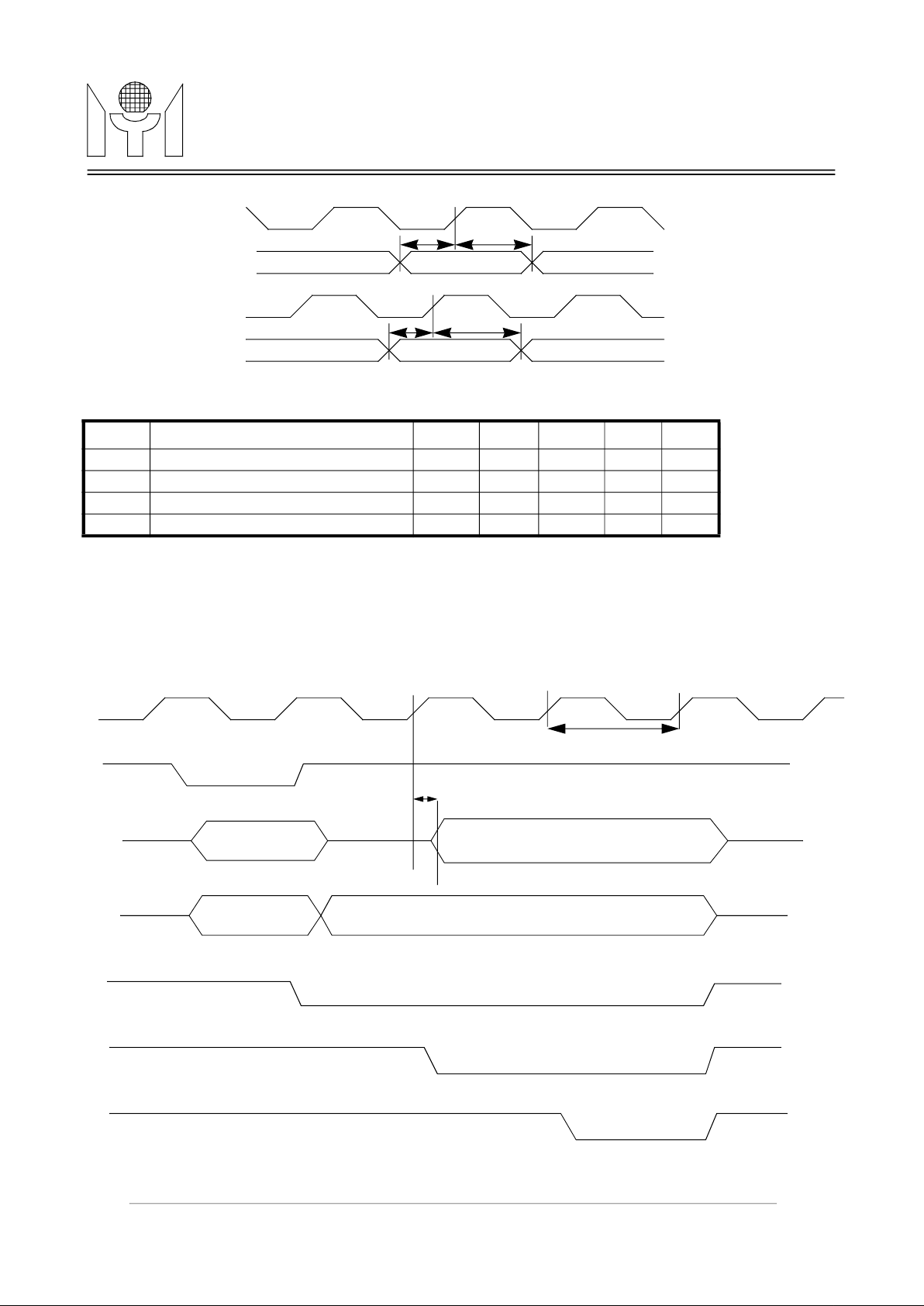
MYSON
BYTE ENABLE
MTD 800
TECHNOLOGY
RXC
CRS,RXD
RXDV
TXC
TXEN
TXD
Symbol Parameter Min. Typ. Max. Unit Note
T1 MII input setup time 10 nS
T2 MII input hold time 10 nS
T3 MII output setup time 20 35 nS
T4 MII output hold time 5 20 nS
5.2.2 PCI Timi ng
T1
T2
Valid
T3
T4
Valid
(Preliminary)
• Read Cycle
PCICLK
FRAME#
AD{31:0]
CBE#[3:0]
IRDY#
DEVSEL#
ADDRESS
Read Cmd
T1
T2
DATA
TRDY#
40/42 MTD800 Revision 0.0 07/20/1999
Page 41
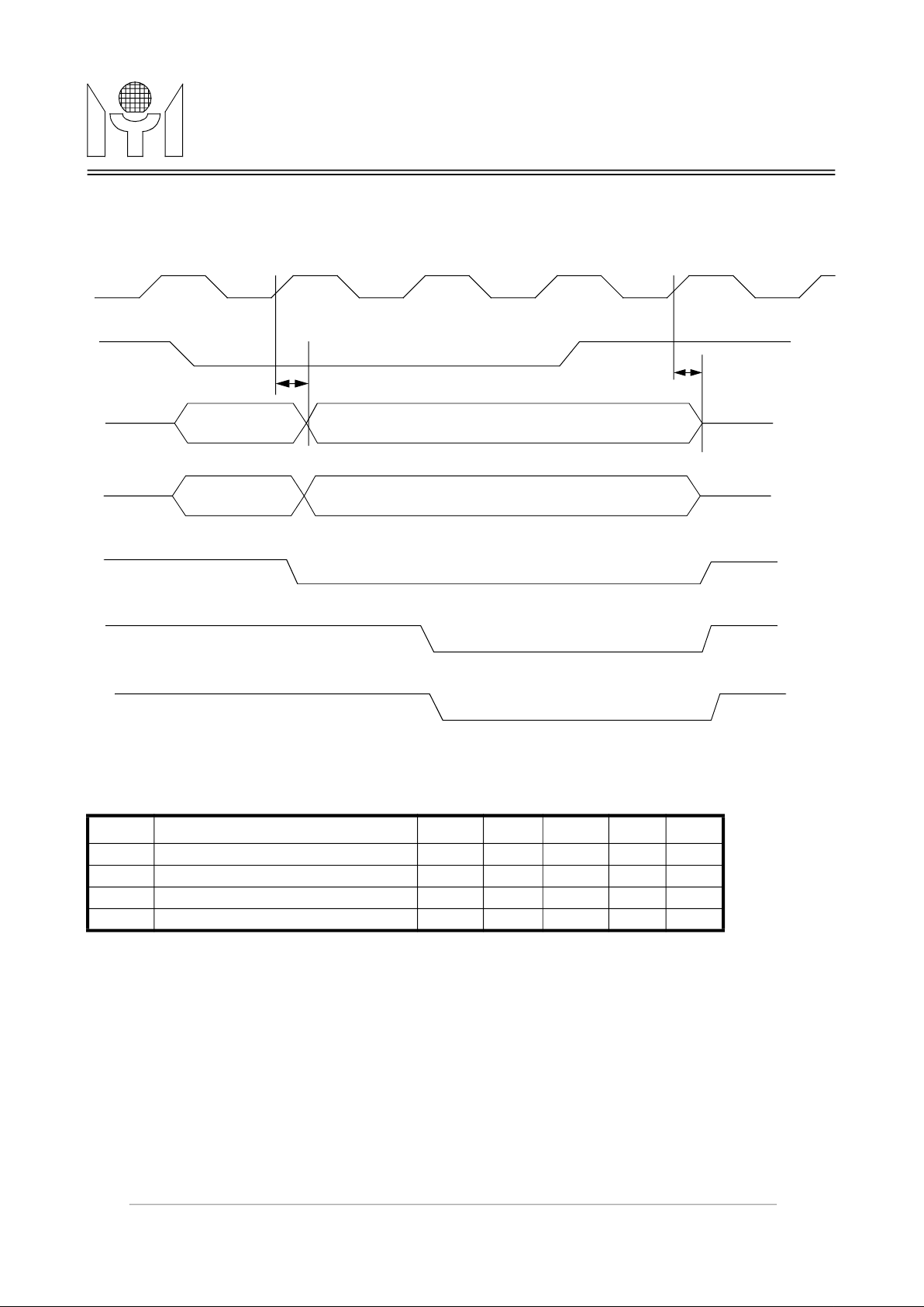
MYSON
PCI CLK Cycle Time
CLK to Signal Valid Delay
Input Setup Time to CLK
Input Hold Time to CLK
BYTE ENABLE
MTD 800
• Write Cycle
PCICLK
FRAME#
AD{31:0]
CBE#[3:0]
IRDY#
TECHNOLOGY
T3
ADDRESS
Write Cmd
(Preliminary)
T4
DATA
DEVSEL#
TRDY#
Symbol Parameter Min. Typ . Max. Unit Note
T1
T2
T3
T4
30 40 nS
2 11 nS
7 nS
0 nS
41/42 MTD800 Revision 0.0 07/20/1999
Page 42

MYSON
6.0 PACKA GE DIMENSION
1.Dimension D1 & E1 do not include mold protrusion.
3.Controlling dimension : Millimeter.
MTD 800
TECHNOLOGY
6.1 128 pin PQFP
103
128
1 38
y
See Detail A
Seating Plane
(Preliminary)
D
1
D
65102
64
1
E
E
39
e
See Detail B
B
A
A1 A2
B
Symbol
Note:
But mold mismatch is included. Allowable protrusion is .25mm/.010” per side.
2.Dimension B does not include dambar protrusion. Allowable dambar protrusion .08mm/.003”. Total in excess of the B dimemsion at maximum material
condition. Dambar cannot be located on the lower radius or the foot.
Dimension in inch Dimension in mm
Min Norm Max Min Norm Max
A - - 0.134 - - 3.40
A1 0.010 - - 0.25 - A2 0.107 0.112 0.117 2.73 2.85 2.97
B 0.007 0.009 0.011 0.17 0.22 0.27
C 0.004 - 0.008 0.09 - 0.20
D 0.906 0.913 0.921 23.00 23.20 23.40
D
0.783 0.787 0.791 19.90 20.00 20.10
1
E 0.669 0.677 0.685 17.00 17.20 17.40
E
0.547 0.551 0.555 13.90 14.00 14.10
1
e 0.020 BSC 0.50 BSC
L 0.029 0.035 0.041 0.73 0.88 1.03
L1 0.063 BSC 1.60 BSC
y - - 0.004 - - 0.10
o
z
-
0
7o0
o
-
o
7
Gage Plane
L
With Plating
C
z
Base Metal
L1
Detail A
Detail B
42/42 MTD800 Revision 0.0 07/20/1999
 Loading...