

Page 1

MYSON
Double scan capability for interlaced input.
MTL002
TECHNOLOGY
(Rev. 0.95)
XGA Flat Panel Controller
FEATURES
General
• Auto configuration of sampling clock frequency, phase, H/V center, as well as white ba lance.
• Auto detection of present or non-present or over range sync signals and their polarities.
• Composite sync separation and odd/even field detection of interlaced video.
• No external memory required.
• On-chip output PLL provide clock frequency fine-tune (inverse, duty cycle and delay).
• Selection of serial 2-wire I
• 3.3V supplier, 5V I/O tolerance in 208-pin PQFP package.
Input Processor
• Single RGB (24-bit) or Dual RGB (48-bit) input rates up to 100MHz.
• Support both non-interlaced and interlaced RGB graphic input signals.
• YUV 4:2:2 or YUV 4:1:1 (CCIR601) interlaced video input.
• Glue-less connection to Philips SAA711x digital video decoder.
• Built-in YUV to RGB color space converter.
• Compliant with digital LVDS/PanelLink TMDS input interface.
• PC input resolution up to XGA 1024x768 @85Hz.
2
C or 3-wire serial or 8-bit direct host interface to 8-bit MCU.
Video Processor
• Independent programmable Horizontal and Vertical scaling up ratios from 1 to 32
• Flexible de-interlacing unit for digital YUV video input data.
• Zoom to full screen resolution of de-interlaced YUV video data stream.
• Built-in programmable gain control for white balance alignments.
• Built-in programmable 8-bit gamma correction table.
• Built-in programmable temporal color dithering.
• Built-in programmable interpolation look-up table.
• Support smooth panning under viewing window change.
Output Processo r
• Single pixel (18/24-bit) or Dual pixel (36/48-bit) per clock digital RGB output.
• Built-in output timing generator with programmable clock and H/V sync.
• Support VGA/SVGA/XGA display resolution.
• Overlay input interface with external OSD controller.
•
GENERAL DESCRIPTION
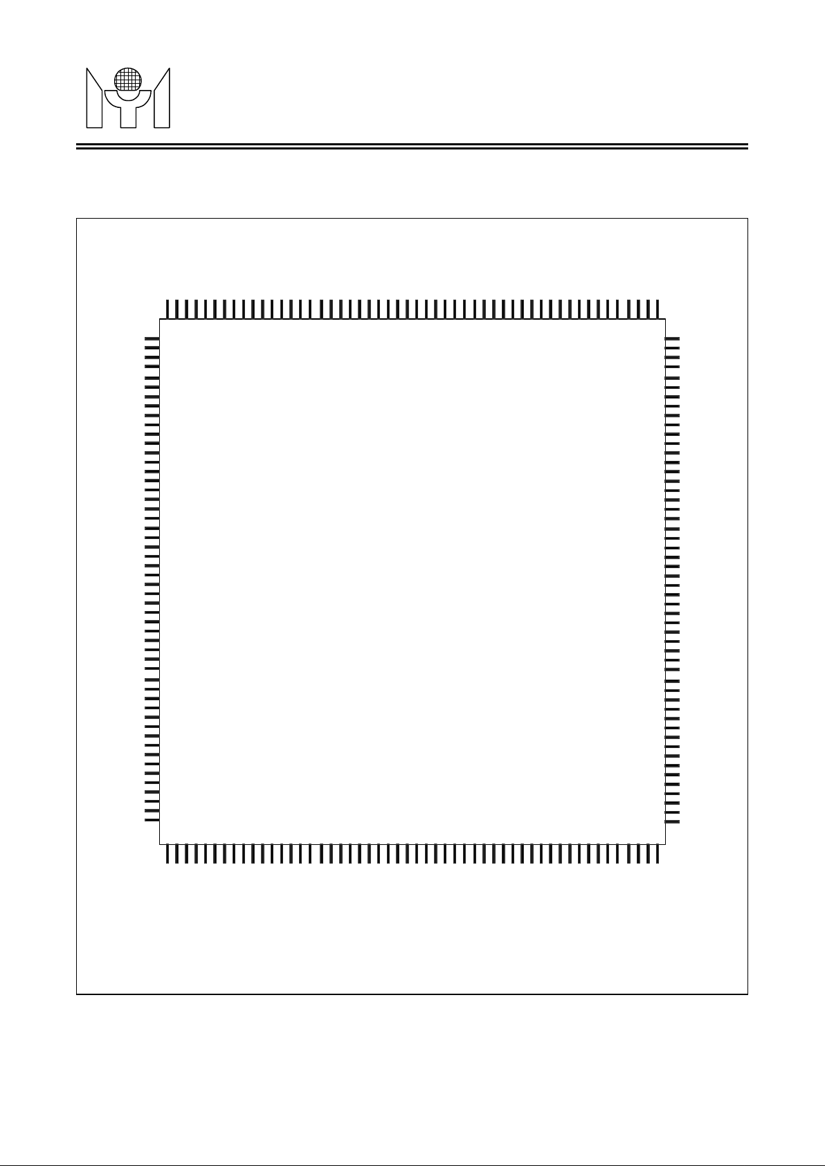
The MTL002 Flat Panel Display (FPD) Controller is an input format converter for TFT-LCD Monitor or LCD
TV application which accepts 15-pin D-sub RGB graphic signals (through ADC), YUV sign als from digital
video decoder or digital RGB graphic signals from PanelLink TMDS receiver. It includes a RGB/YUV input
processor, video scaling up processor, OSD input interface and output display processor in 208-pin PQFP.
Revision 0.95 - 1 - 2000/06/14
Page 2
MYSON
video
RGB
8-bit MCU
MTV130
OSD
Decoder
S-Video
Generator
MTL002
TECHNOLOGY
BL OCK DIAGRAM
Digital
PC
YUV
Input
RGB
Input
Auto
Calibration
YUV
to
RGB
Mode
Detect
Zoom
Buffer
Host
Interface
To I2C Bus
Scale
Up
Gain
Control
Dithering
Gamma
Correct
(Rev. 0.95)
To external OSD
OSD
&
Output
MUX
Display
Timing
RGB
output
APPLICA TIONS
LVDS/PanelLink
TMDS Receiver
D-sub RGB
graphic signals
Composite/
ADC1
ADC2
Digital
Video
MTL002
FPD Monitor
Controller
MTV212
TFT-LCD
Flat Panel
This datasheet contains new product information. Myson Technology reserves the rights to modify the product specification without
notice. No liability is assumed as a result of the use of this product. No rights under any patent accompany the sale of the product.
Revision 0.95 - 2 - 2000/06/14
Page 3
MYSON
052* PVSS
051* AD6
050* AD7
049* ALE
048* DVDD
047* B1OUT3
NC *105
NC *106
NC *107
TDIE *108
PVSS *109
B1IN1 *110
MTL002
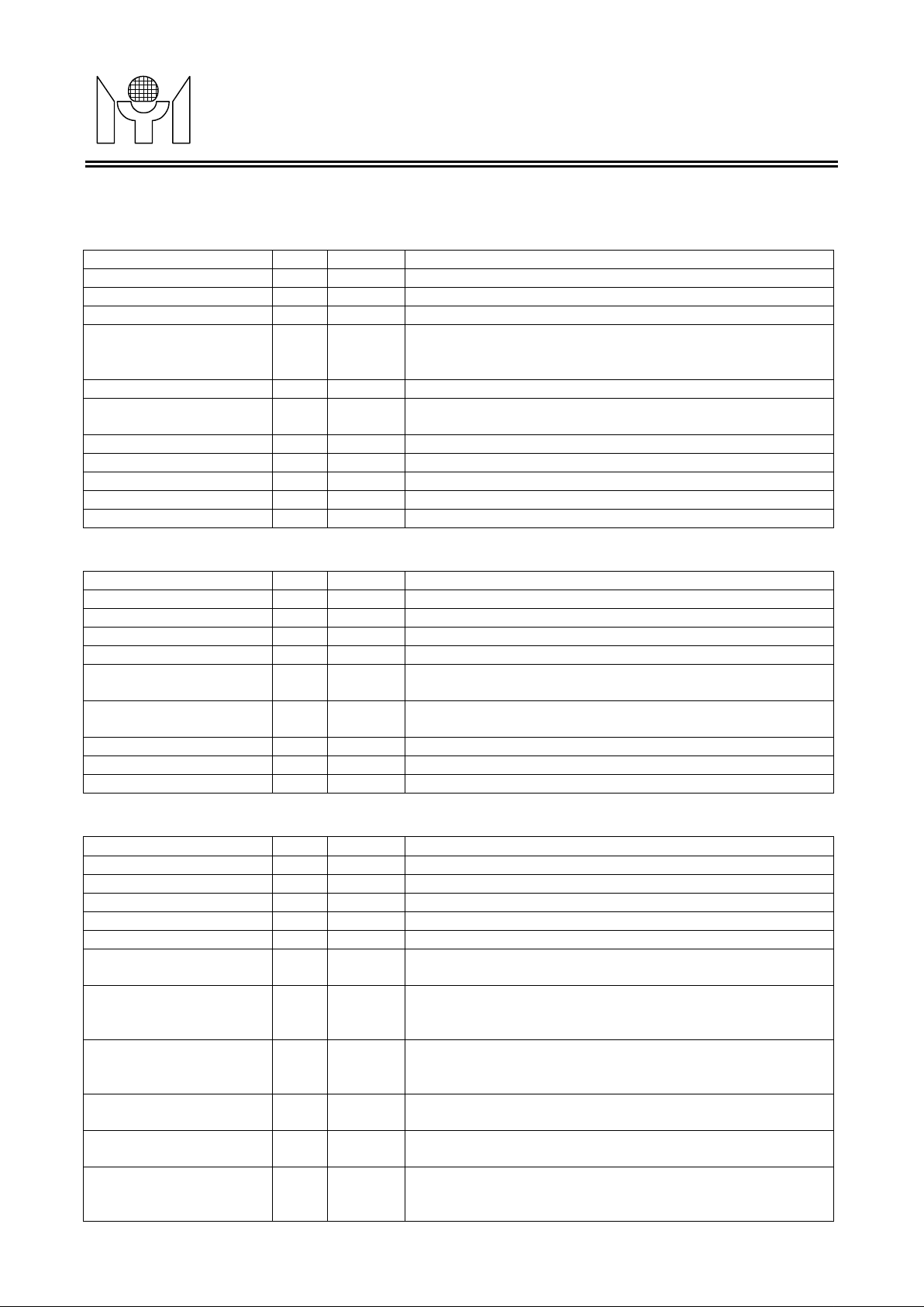
1. PIN CONNECTION
AVDD *152
XO *153
XI *154
NC *157
NC *158
GPIO1 *159
GPIO0 *160
PVSS *161
OHSYNC *162
OCLK *163
OVSYNC *164
G2IN7 *165
G2IN6 *166
G2IN5 *167
G2IN4 *168
G2IN3 *169
G2IN2 *170
G2IN1 *171
DVDD *172
EXTDCLK2 *173
DVSS *174
EXTDCLK1 *175
PVDD *176
G2IN0 *177
G2OUT0 *178
PVSS *179
G2OUT1 *180
G2OUT2 *181
G2OUT3 *182
DVDD *183
G2OUT4 *184
G2OUT5 *185
G2OUT6 *186
G2OUT7 *187
DVSS *188
R2OUT0 *189
R2OUT1 *190
R2OUT2 *191
R2OUT3 *192
NC *193
RSTZ *194
PVDD *195
G1OUT0 *196
NC *197
G1OUT1 *198
PVSS *199
G1OUT2 *200
G1OUT3 *201
G1OUT4 *202
G1OUT5 *203
PVDD *204
BUSSEL0 *205
BUSSEL1 *206
PVSS *208
NC *207
AVSS *155
005* PVSS
004* OSDINT
003* NC
002* NC
TECHNOLOGY
G1IN7 *133
G1IN6 *134
G1IN5 *135
G1IN4 *136
G1IN3 *137
G1IN2 *138
G1IN1 *139
G1IN0 *140
VSYNC1 *141
IPCLK1 *142
RAWHS *143
VPHREF *144
HSYNC1 *145
VPODD *146
VPCREF *147
IPCLK2 *148
HSYNC2 *149
VSYNC2 *150
PVDD *151
MTL002
(208-pin PQFP)
024* DDCLK
023* DVSS
022* NC
021* GPIO2
020* GPIO3
019* NC
018* OSDEN
017* OSDBLU
016* DVDD
015* OSDGRN
014* OSDRED
013* DVSS
012* R1OUT3
011* R1OUT2
010* DVDD
009* R1OUT1
008* R1OUT0
007* G1OUT7
006* G1OUT6
R1IN1 *128
TMDSSEL *129
RGBSEL *130
DVDD *131
R1IN0 *132
029* DHSYNC
028* DVSYNC
027* DVDD
026* DHCLK
025* DDEN
R1IN4 *123
R1IN3 *124
CLAMP *125
R1IN2 *126
DVSS *127
034* HRDZ
033* NC
032* DVSS
031* HWRZ
030* DOEZ
R2IN1 *118
R2IN0 *119
R1IN7 *120
R1IN6 *121
R1IN5 *122
039* PVSS
038* R1OUT5
037* R1OUT4
036* DVSS
035* DVDD
R2IN6 *113
R2IN5 *114
R2IN4 *115
R2IN3 *116
R2IN2 *117
044* B1OUT1
043* B1OUT0
042* PVDD
041* R1OUT7
040* R1OUT6
(Rev. 0.95)
B1IN0 *111
R2IN7 *112
046* B1OUT2
045* DVSS
104* NC
103* NC
102* DVSS
101* NC
100* DVDD
099* B1IN2
098* B1IN3
097* B1IN4
096* B1IN5
095* B1IN6
094* B1IN7
093* B2IN0
092* B2IN1
091* PVDD
090* B2IN2
089* B2IN3
088* B2IN4
087* B2IN5
086* B2IN6
085* B2IN7
084* PVSS
083* B2OUT7
082* B2OUT6
081* B2OUT5
080* B2OUT4
079* DVDD
078* B2OUT3
077* B2OUT2
076* B2OUT1
075* DVSS
074* B2OUT0
073* R2OUT7
072* DVDD
071* R2OUT6
070* R2OUT5
069* R2OUT4
068* DVSS
067* IRQ
066* AD2
065* AD1
064* AD0
063* HCSZ
062* PVDD
061* B1OUT7
060* B1OUT6
059* B1OUT5
058* B1OUT4
057* PVSS
056* AD3
055* AD4
Revision 0.95 - 3 - 2000/06/14
Page 4
MYSON
Input source HSYNC or Input Sync On Green
tri_state all Display port
MTL002
TECHNOLOGY
(Rev. 0.95)
2. PIN DESCRIPTION
ADC1 Inpu t Inter f ac e (RGB or TMDS Input Data)
Name Type Pin# Description
IPCLK1 I 142 Input pixel clock 1
VSYNC1 I 141 Input Vertical s ync 1
HSYNC1/CS1 I 145 Input Horizontal or Composite sync 1
R1IN[7:0] I 120-124,
126,128,
132
G1IN[7:0] I 133-140 Green channel or TMDS input data (Single/Dual ADC)
B1IN[7:0] I 94-99,
110-111
RAWHS/SOG I 143
TDIE I 108 TMDS digital input enable
RGBSEL O 130 Input select. 1:RGB input, 0:YUV input
TMDSSEL O 129 TMDS input select, active high
CLAMP O 125 Clamp pulse output for ADC
Red channel or TMDS input data (Single/Dual ADC)
Blue channel or TMDS input data (Single/Dual ADC)
ADC2 Input Int er f ac e (YUV or RGB or TMDS Inpu t Data)
Name Type Pin# Description
IPCLK2 I 148 Input pixel clock 2
VSYNC2 I 150 Input Vertical s ync 2
HSYNC2/CS2 I 149 Input Horizontal or Composite sync 2
R2IN[7:0]/YIN[7:0] I 112-119 Red or Y channel or TMDS input data (Single/Dual ADC)
G2IN[7:0] I 165-171,
177
B2IN[7:0]/UVIN[7:0] I 85-90,
92-93
VPHREF I 144 Input Video Horizontal reference signal
VPCREF I 147 Input Video clock enable
VPODD I 146 Input Video ODD/EVEN field signal
Green channel or TMDS input data (Single/Dual ADC)
Blue or UV channel or TMDS input data (Single/Dual ADC)
Displ ay Outp ut Interface
Name Type Pin# Description
DDEN O 25 Display data output enable
DVSYNC O 28 Display Vertical sync output
DHSYNC O 29 Display Horizontal sync output
DDCLK O 24 Display output clock
DHCLK O 26 Display half rate output clock
DOE# I 30 Display port output enable, “1” will
output signals
R1OUT[7:0] O 41-40
38-37,
12-11,9-8
G1OUT[7:0] O 7-6,
203-200,
198,196
B1OUT[7:0] O 61-58,47,
46,44,43
R2OUT[7:0] O 73,71-69,
192-189
G2OUT[7:0] O 187-184,
182-180,
178
Revision 0.95 - 4 - 2000/06/14
Red output even data , bit[7:2] for 6-bit panel
Green output even data , bit[7:2] for 6-bit panel
Blue output even data , bit[7:2] for 6-bit panel
Red output odd data , bit[7:2] for 6-bit panel
Green output odd data , bit[7:2] for 6-bit panel
Page 5
MYSON
Vertical sync for external OSD
Horizontal sync for external OSD
OSD intensity input
OSD overlay enable
Oscillator frequency input
Oscillator frequency output
Bit 0: ADHS, Horizontal sync for A/D converter
MTL002
TECHNOLOGY
B2OUT[7:0] O 83-80,
78-76,74
Blue output odd data , bit[7:2] for 6-bit panel
(Rev. 0.95)
Host Interface
Name Type Pin# Descrip tio n
RST# I 194 System reset input, active low.
AD[7:0] I/O 50-51,
54-56,
66-64
HWR# I 31 Host write strobe, active low
HRD# I 34 Host read strobe, active low
ALE I 49 Host address latch enable for 8-bit direct bus
HCS# I 63 Host chip select
BUSSEL[1:0] I 206,205 Bus mode selection. 0x: 3-wire bus, 10: I2C bus,
IRQ O 67 Interrupt request output
The address and data bus of 8-bit direct interface or
2-wire I2C / 3-wire series bus
Bit 2: SDAO, 3-wire serial bus data out
Bit 1: SDA, serial bus data / 3-wire serial bus data in
Bit 0: SCK, serial bus clock
11: 8-bit direct bus
OSD Interf ac e
Name Type Pin# Description
OCLK O 163 Clock for external OSD
OVSYNC O 164
OHSYNC O 162
OSDRED I 14 OSD red input
OSDGRN I 15 OSD green input
OSDBLU I 17 OSD blue input
OSDINT I 4
OSDEN I 18
Other Interface
Name Type Pin# Description
XI I 154
XO O 153
EXTDCLK1 I 175 External display clock input 1
EXTDCLK2 I 173 External display clock input 2
GPIO[3:0] I/O 20-21,
General purpose I/O or
159-160
Bit 1: ADVS, Vertical sync for A/D converter
Default: Input direction
NC - 1-3, 19,
22, 33,
53, 101,
103-107,
156-158,
193, 197,
207
No connection
3.3V Power and Grou n d
Name Pin# Descrip tio n
DVDD 10, 16, 27, 35, 48, 72, 79, 100, 131, 172, 183 Digital power 3.3V
DVSS 13, 23, 32, 36, 45, 68, 75, 102, 127, 174, 188 Digital ground
PVDD 42, 62, 91, 151, 176, 195, 204 Pad power 3.3V
PVSS 5, 39, 52, 57, 84, 109, 161, 179, 199, 208 Pad ground
Revision 0.95 - 5 - 2000/06/14
Page 6

MYSON
MTL002
TECHNOLOGY
AVDD 152 Analog power 3.3V
AVSS 155 Analog ground
(Rev. 0.95)
Revision 0.95 - 6 - 2000/06/14
Page 7

MYSON
The Digital RGB input port works just in the same way as Sec 3.1.1 except that pin
With a flexible single or double pixel input interface, the supported format is up to true color, includi ng 18
In general, the synchronous HSYNC input for HSYNC1 or HSYNC2 generated by an ADC may have a very
In this mode, only one field is displayed at the time. First field and second field are toggling displayed. The
interpolating the neighboring lines. This mode has a generally good quality for still and moving pictures.
MTL002
TECHNOLOGY
(Rev. 0.95)
3. FUNCTIONAL DESCRIPTION
3.1 Input Process or
General Descrip t io n
The function of Input Interface is to provide the interface between MTL002 and external in put devices. It can
process non-interlaced and interlaced RGB graphic input, YUV video input, and digita l RGB in put compliant
with digital LVDS/PanelLink TMDS interface. It also contains the built-in YUV to RGB color space converter.
3.1.1 RGB Input Format
The RGB input port works in two modes: Single Pixel mode (24 bits) and Double Pixel mode (48 bits). For
Single Pixel mode, either ports R/G/B1IN[7:0] or R/G/B2IN[7:0] selected by Reg.16h/D0 can be chosen to be
internally sampled. For the Double Pixel mode, besides ports R/G/B1IN[7:0], ports R/G/B2IN[7:0] are also
needed. The R/G/B1IN ports are sampled at the rising edge of the RGB input clock, and the R/G/B2IN ports
are sampled at the falling edge.
3.1.2 TMDS Inpu t Form at
“Digital Input Enable
DIEN “ is needed.
bit/pixel or 24 bit/pixel in 1 or 2 pixels/clock mode.
3.1.3 YUV Input Form at
The YUV input port supports interlaced video data from the most common video decoder ICs like SAA711x.
The 16 bit data bus is shared with ports R2IN[7:0] and B2IN[7:0]. The 16 bit data is sampled at the rising
edge of the shared video clock VPCLK when the shared data enable HREF is active. The formats supported
are YUV4:1:1 and YUV4:2:2 with CCIR601 standard.
3.1.4 Inpu t HSYNC Path
In addition to the pins HSYNC1/2, MTL002 provides another pin RAWHS to support the Sync Processor.
narrow pulse width and a different polarity comparing to the original HSYNC provided by the source. The
RAWHS input provides the path of original HSYNC connection to MTL002, thus making Sync Processor in
MTL002 working properly.
3.1.5 YUV to RGB Convert er
Is used to convert YCbCr format into RGB format. The basic equations are as follows:
R = Y + 1.371(Cr – 128)
G = Y – 0.698(Cr – 128) – 0.336(Cb – 128)
B = Y + 1.732(Cb - 128)
3.1.6 De-int erlace mod e
For the interlace input, MTL002 features several de-interlacing algorithms for processing interlaced video
data depending on the type of input images.
¨ Togg le Mode
missing lines are calculated by duplicating the neighboring lines. This m ode gives good quality for moving
pictures.
¨ Spatial Mode
In this mode, two fields are toggling displayed just like the Toggle mode. The m issing lines are calculated by
Revision 0.95 - 7 - 2000/06/14
Page 8

MYSON
inputs presence check, frequency counting, polarity detection and control. It contains
MTL002 can measure VSYNC/HSYNC frequency counted in proper clock and save the information in
input sample registers to aid in centering the screen automatically.
s phase and frequency.
s phase and frequency. MTL002
This advanced function helps Firmware to analyze ADC performance. Usually Firmware can use the
MTL002
TECHNOLOGY
(Rev. 0.95)
3.1.7 Sync Processo r
The V/H SYNC processing block performs the functions of Composite signal separation/insertion, SYNC
a de-glitch circuit to
filter out any pulse shorter than one OSC period which is treated as noise am ong V/H SYNC pulses.
¨ V/H SYNC Frequency Cou n ter
register. Users can read the figure and calculate VSYNC/HSYNC frequency as following formulas:
f
= f
= f
osc
osc
/ N
/ N
vsync
f
hsync
,Where f
f
f
N
N
¨ V/H SYNC Pres en ce Check
vsync
hsync
osc
vsync
hsync
51/256
vsync
58
hsync
: VSYNC frequency
: HSYNC frequency
: oscillator clock with 14.31818 MHz
: counted number of VSYNC
: counted number of HSYNC
This function checks the input VSYNC, where Vpre flag is set when VSYNC is over 40Hz or cleared when
VSYNC is under 10Hz and the input HSYNC, where Hpre flag is set when HSYNC is over 10Khz or cleared
when HSYNC is under 10Hz.
the
¨ V/H Polarity Detect
This function detects the input VSYNC/HSYNC high and low pulse duty cycle. If the high pulse duration is
longer than that of low pulse, the negative polarity is asserted; otherwise, positive polarity is asserted.
¨ Compos it e SYNC separatio n/ins erti on
MTL002 continuously monitors the input HSYNC. If the input VSYNC can be extracted from it, a CVpre flag is
set. MTL002 can insert HSYNC pulse during Composite VSYNC’s active time and the insertion frequency
can adapt to the original HSYNC’s.
3.1.8 Auto Tune
Auto Tune function consists of Auto Position which automatically centering the screen an d A uto Calibration
which contains Phase Calibration, Histogram, Min/Max Value, and Pixel Grab that are described in the
following paragraphs. With such auto adjustment support it is possible to measure the correct phase,
frequency, gain, and offset of ADC. The horizontal and vertical back porches of input image and the
horizontal and vertical active regions can also be measured. Firmware can adjust input image registers
automatically by reading Auto Tune’s registers in single or burst mode.
¨ Auto Position
MTL002 provides Horizontal/Vertical back porch and active region values. Users can use these values to set
¨ Phase Calibration
MTL002 provides Auto Calibration registers to measure the quality of current ADC’
The biggest Auto Calibration registers value means the right value of ADC’
has two kinds of algorithms to calculate Auto Calibration’s value. One is traditional Difference method,
another is MYSON’s proprietary method. The latter one is recommended for a better performance.
¨ Histogram
Histogram is the total number of input pixels below/above one threshold value for individual R, G, B colors.
information to measure ADC’s noise margin, adjust its offset and gain, or even aid in the mode detection.
¨ Min /Max Value
Min/Max value is the minimum or maximum pixel value within the specified input active image region for each
RGB channel. This information is usually used to adjust ADC’s offset and gain.
Revision 0.95 - 8 - 2000/06/14
Page 9

MYSON
MTL002
TECHNOLOGY
¨ Pixel Grab
Pixel Grab means user can grab a single input pixel at any one point. The position of the point can be
programmed by the user. This is another traditional method to measure ADC’s phase and frequency.
(Rev. 0.95)
Revision 0.95 - 9 - 2000/06/14
Page 10
MYSON
MTL002
TECHNOLOGY
(Rev. 0.95)
3.2 Video Proc ess o r
General Descrip t io n
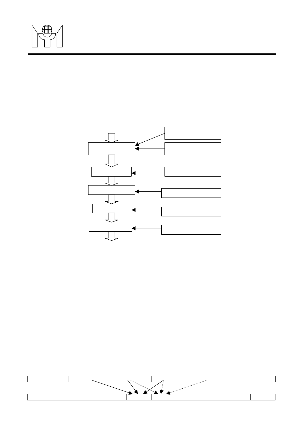
MTL002 possesses a powerful and programmable video processor b y providing the following functions:
Scaling Up, Gain Control, Brightness Control, Gamma Correction, and Dithering Control.
The block diagram of Video Processor is as follows:
Fig. 3.2.1 Video Processor Block Diagram
SCALING
3.2.1 Scaling
MTL002 provides scaling function ranging from 1 to 32 for up scaling, and for both horizo ntal and vertical
GAIN
BRIGHTNESS
Scaling Factor
Interpolation Table
Gain Factor
Brightness Factor
GAMMA
DITHERING
processing. For scaling up, both horizontal and vertical processing, MTL002 provides four methods:
¨ Pass Mode: Image will be passed through without taking scaling factor into account.
¨ Dupli cate Mode: Image will be scaled up based on the scaling factor. Every point of output image
comes from the input. In this method, the output image will have a good contrast but the picture could be
non-uniformed.
¨ Bilin ear Mode: Image will be scaled up based on the scaling factor. Every point of output image data
will be filtered by bilinear filter. In this method, the output image will have a good scaling quality but the
picture could be blurred.
¨ Interpol atio n Table Mode: Image will be scaled up based on the scaling factor. The user-defined filter
will filter every point of output image data. In this mode, every output point is calculated based on the 3
input points.
Gamma Table
Dithering Table
Input pixels:
I
k-1
Output pixels:
Revision 0.95 - 10 - 2000/06/14
A
Y
l-1
I
k
l
B
l
Y
l
I
k+1
C
l
Y
l+1
Page 11

MYSON
programming the gain and brightness coefficients. This adjustment is applied to RGB colors individually.
Gamma Correction is used to compensate the non-linearity of LCD display panel. MTL002 contains an 8-bit
true color (8 bits per color) or high color (6 bits per color) display.
Output processor provides the interface for both LCD panel and OSD controller. The output frame rate must
be equal to the input frame rate and output display time must be equal to input display time since there is no
MTL002
TECHNOLOGY
,where Yl=Al*I
3.2.2 Gain/Bright ness Control
MTL002 provides Gain and Brightness control to adjust the contrast and brightness of output color by
Auto-white balance can be achieved by using this function.
3.2.3 Gamma Correction
Gamma table to fix this phenomenon.
3.2.4 Color Dithering
MTL002 supports
In the latter case, users can turn on dithering function to avoid artificial contour due to truncation. The
dithering function works in two modes:
¨ Static dith ering: Dithering coefficient is f ixed.
¨ Temporal dithering: Dithering coefficient is time dependent.
k-1+Bl*Ik+Cl*Ik+1
and A, B, C are the scaling factors from interpolation table
Fig. 3.2.2 Scaling filter
(Rev. 0.95)
3.3 Outpu t Process or
General Descrip t io n
frame buffer present.
Revision 0.95 - 11 - 2000/06/14
Page 12
MYSON
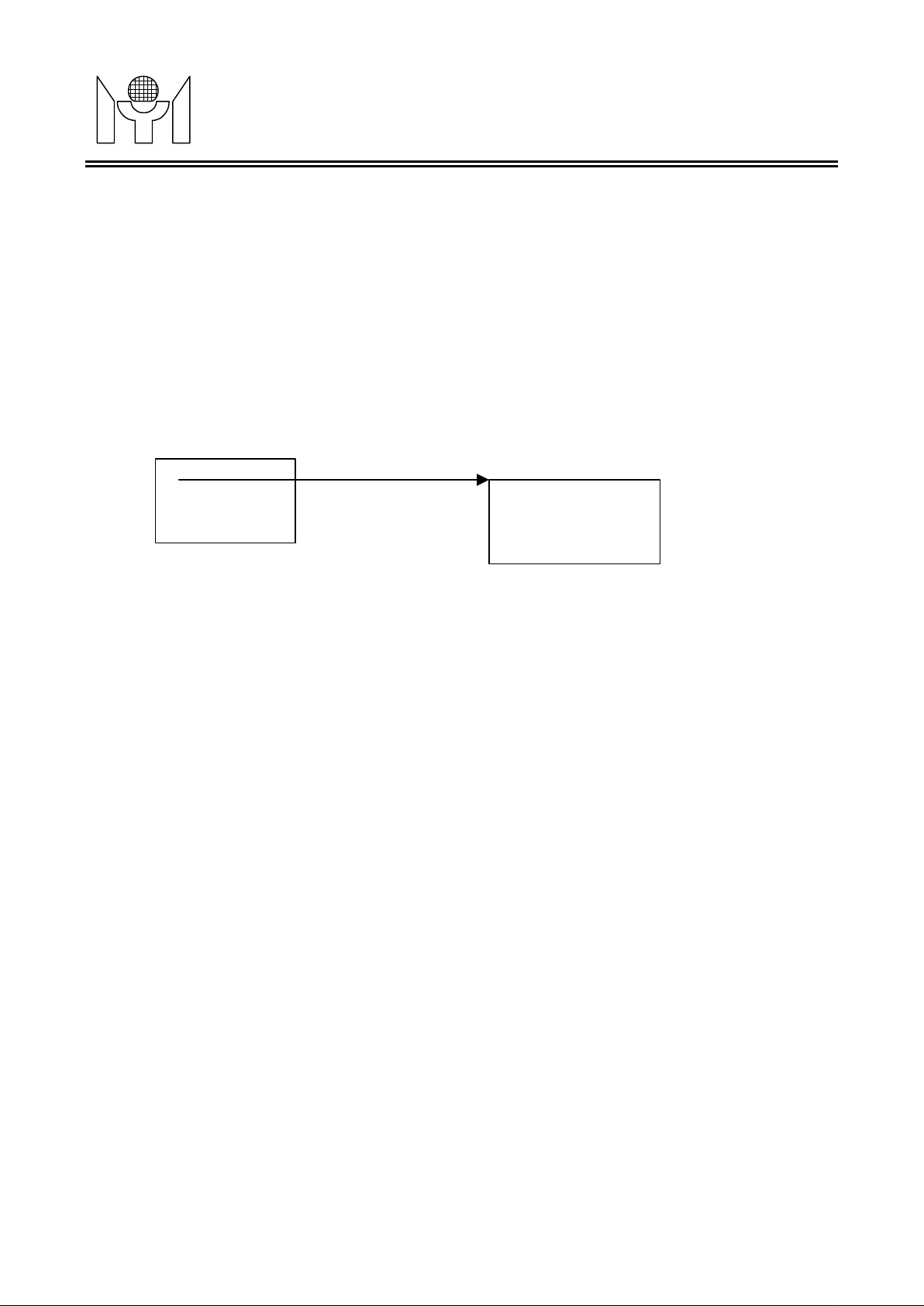
Because of no frame buffer, output displaying timing is locked by input timing and output frame rate is equal
to input frame rate. Users must program output timing and lock position to make sure that line buffer will not
overflow or underflow. MTL002 can automatically calculate Display Horizontal Total count to make the output
timing calculation easier. MTL002 also provides line buffer overflow/underflow status for calibrating lock
3.2.2 Display Timing modes
with a resolution of 6/8 bits per color. These two ports are PORT1 and PORT 2 respectively.
MTL002
TECHNOLOGY
3.3.1 Display Timing Generation
position.
Input Frame Output Frame
X
X: lock position
(Rev. 0.95)
Fig.
3.3.2 OSD Overl ay
MTL002 allows the integration of overlay data with the scaled output pixel stream. It provides a fully
compatible OSD interface. Individual OSD clock, OSD HSYNC and OSD VSYNC are sent to external OSD
device. MTL002 receives OSD Enable, OSD Red, OSD Green, OSD Blue, and OSD Intensity from external
OSD device.
3.3.3 RGB Outpu t Form at
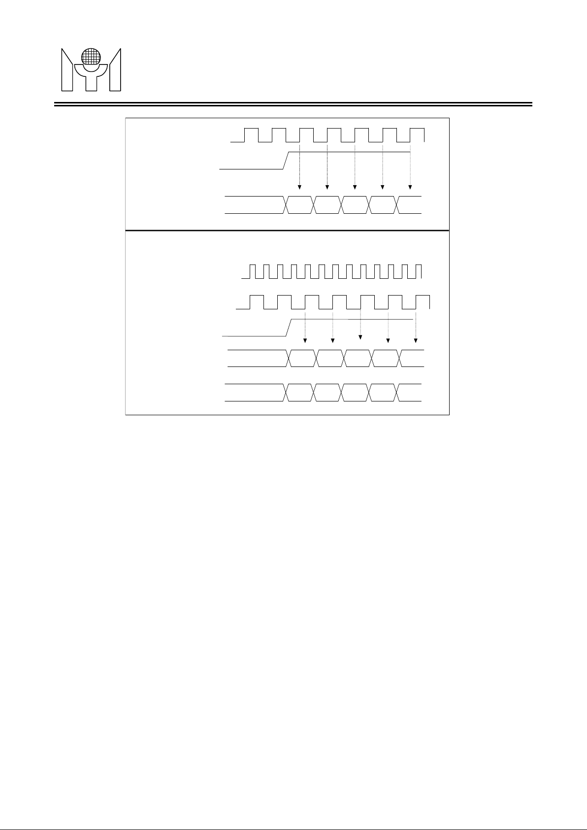
MTL002 output interface consists of two pixel ports, each containing Red, Green, and Blue color information
The control signals for the output port are display horizontal sync signal (DHSYNC), display vertical sync
signal (DVSYNC) and display data enable signal (DDEN).
All the signals mentioned above are synchronous to the output clock. The output timing relative to the active
edge of the output clock is programmable.
There are two RGB output formats:
¨ Singl e Pixel Mode
Is designed to support TFT panels with single pixel input. Only PORT1 is active. The frequency of DCLK is
equal to internal display clock.
¨ Dual Pixel Mode
Is designed to support TFT panels with dual pixel input. PORT1 and PORT2 are used. The first pixel is at
PORT1, with the second at PORT2.
Revision 0.95 - 12 - 2000/06/14
Page 13
MYSON
R1OUT/G1OUT
R1OUT/G1OUT
R2OUT/G2OUT
SINGLE POR T
3.2.3 Display Data Timing
MTL002
TECHNOLOGY
DDCLK
DDEN
000 rgb0 rgb1 rgb2 rgb3 rgb4
000 rgb0 rgb2 rgb4 rgb6 rgb8
DUAL PORT
/B1OUT
DDCLK
DHCLK
DDEN
/B1OUT
(Rev. 0.95)
/B2OUT
Fig.
000 rgb1 rgb3 rgb5 rgb7 rgb9
3.5 Host Inter fac e
Revision 0.95 - 13 - 2000/06/14
Page 14
MYSON
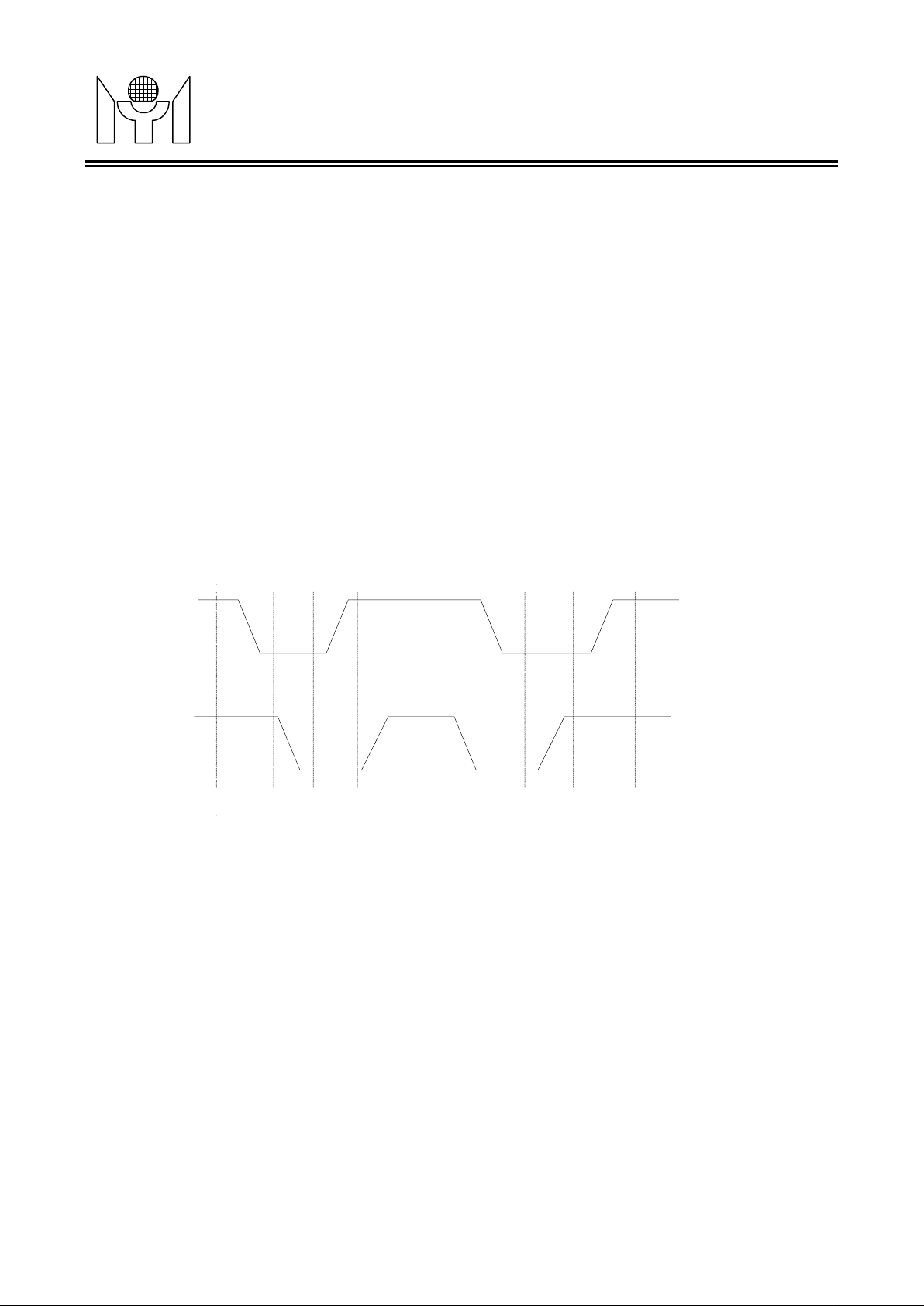
means a LOW to HIGH transition of SDA when SCK is high. And data of SDA only changes when SCK is low.
C interface supports Random Write, Sequential Write, Current Address Read, Random Read and
For Random Write operation, it contains the slave address with R/W bit set to 0 and the word address which
is comprised of eight bits that provides the access to any one of the 256 bytes in the selected memory range.
MTL002
TECHNOLOGY
General Descrip t io n
The main function of Host Interface is to provide the interface between MTL002 and externa l CPU by 2-wire
I2C Bus or 3-wire series Bus or 8-bit Direct Bus selected by the input pins BUSSEL[1:0]. It can generate all
the I/O decoded control timing to control all the registers in MTL002. The other function is Screen Write,
which allows users to clear frame buffer, and display output as well.
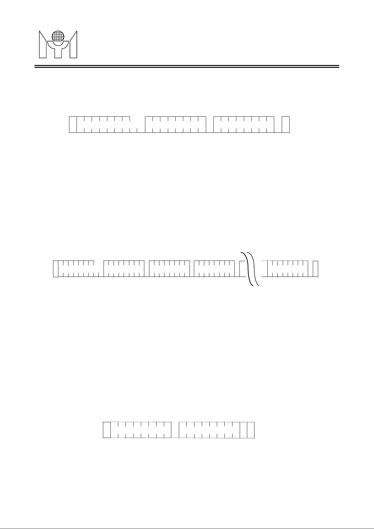
3.5.1 I2C Serial Bus
The I2C serial interface use 2 wires, SCK (clock) and SDA(data I/O). The SCK is used as the sampling clock
and SDA is a bi-directional signal for data. The communication must be started with a valid START condition,
concluded with STOP condition and acknowledged with ACK condition by receiver.
The I2C bus device address of MTL002 is 0111010x.
AD[0] SCK, serial bus clock.
AD[1] SDA, bi-directional serial bus data.
The START condition means a HIGH to LOW transition of SDA when SCK is high, the STOP condition
Ref. Fig.3.5.1.
(Rev. 0.95)
SDA
SCK
START
Fig. 3.5.1 START, STOP ,and DATA definition
2
The I
Sequential Read operations.
¨ Random Write
Upon receipt of the word address, MTL002 responds with an Acknowledge and waits for the next eight bits of
data again, responding with an Acknowledge, and then the master generates a stop co ndition. Ref. Fig.3.5.2.
DATA
CHANGE
DATA
CHANGE
STOP
Revision 0.95 - 14 - 2000/06/14
Page 15
MYSON
3.5.2 Random Write
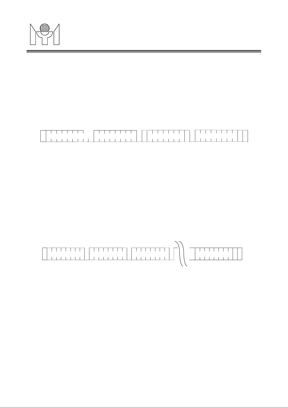
Current Add ress Read
access address is n, the read data should access from address n+1. Upon receipt of the slave address with
bits data. After receiving data
S
MTL002
TECHNOLOGY
S
T
A
R
T
SDA
¨ Sequential Write
The initial step of Sequential Write is the same as Random Write, after the receipt of each word data,
MTL002 will respond with an Acknowledge and then internal address counter will increment by one for next
data write. If the master stops writing data, it will generate stop condition. Ref. Fig. 3.5.3.
T
A
SLAVE
R
ADDRESS
T
SLAVE
ADDRESS
ADDRESS
A
W
C
K
Fig.
WORD
WORD
ADDRESS
DATA n
DATA
A
C
K
DATA n+1
(Rev. 0.95)
S
T
O
P
A
C
K
S
T
O
DATA n+x
P
SDA
A
W
C
K
Fig. 3.5.3 Sequential Write
¨
MTL002 contains an address counter which maintains the last access address incremented by one. If the last
R/W bit set to 1, MTL002 generates an Acknowledge and transmits the eight
the master will generate a stop condition instead of an Acknowledge. Ref. Fig. 3.5.4.
S
T
A
R
ADDRESS
T
SDA
SLAVE
A
C
K
R
A
C
K
DATA
A
C
K
A
C
K
S
T
O
P
A
C
K
Fig. 3.5.4 Current Address Read
Revision 0.95 - 15 - 2000/06/14
Page 16
MYSON
The operation of Random Read allows access to any address. Before the reading data operation, it must
the master issues the start condition, slave address and then the word
address it is to read. After the word address acknowledge, the master generating a start condition again and
slave address with R/W bit is set to 1. MTL002 then transmits the 8 bits of data. Upon the completion of
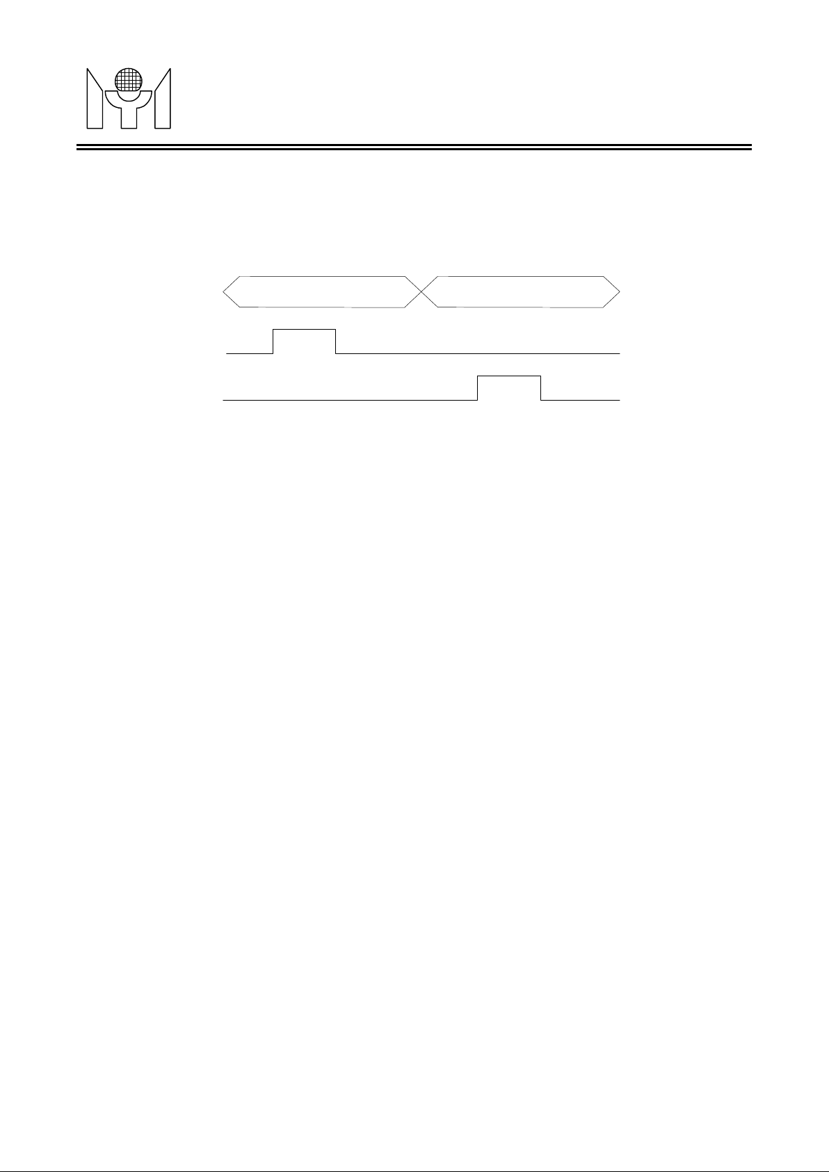
The Direct Bus use AD[7:0], HWR#, HRD#, ALE, HCS# as the interface with host. ALE is used to latch read
S
MTL002
TECHNOLOGY
¨ Random Read
issue a “dummy write” operation —
receiving data, the master will generate a stop condition instead of an Acknowledge. Ref. Fig 3.5.5.
S
T
A
R
T
A
C
K
SLAVE
ADDRESS
A
R
C
K
SDA
T
A
R
T
SLAVE
ADDRESS
WORD
ADDRESS
A
W
C
K
Fig. 3.5.5 Random Read
(Rev. 0.95)
S
T
DATA
O
P
¨ Sequenti al Read
The initial step can be as either Current Address Read or Random Read. The first read data is transmitted in
the same manner as for other read methods. However, the master generates an Acknowledge indicating it
requires more data to read. MTL002 continues to output data for each Acknowledge received. The output
data is sequential and the internal address counter increments by one for next read data. Ref. Fig. 3.5.6.
S
T
A
SLAVE
R
ADDRESS
T
SDA
A
R
C
K
Fig. 3.5.6 Sequential Read
3.5.2 3-wire Serial Bus
The 3-wire serial interface use 3 wires, SCK (clock) and SDA(data I) and SDAO(data O). The SCK is used as
the sampling clock, SDA is an input signal for data, and SDAO is an output signal for data. T he h andshaking
protocol is the same as for the 2-wire I2C serial bus.
DATA n
A
C
K
DATA n+1
DATA n+x
A
C
K
S
T
O
P
AD[0] SCK, serial bus clock.
AD[1] SDA, serial bus data in.
AD[2] SDAO, serial bus data out.
3.5.3 8-bit Direct Bus
or write address from AD[7:0] and HRD#, HWR# to access data. Ref. Fig. 3.5.7.
AD[7:0] Address and data multiplex bus.
Revision 0.95 - 16 - 2000/06/14
Page 17
MYSON
Writing data to Reg. F4h/D2 when
ADVS/ADHS Output con tr ol pro cess
pin to output ADHS which is HSYNC signal decoded from VGA input Composite signal by the
Writing data to F4h/D0 when
HWR/HRD
MTL002
TECHNOLOGY
HRD# CPU re ad data strobe, Active Low.
HWR# CPU write data strobe, Active Low.
ALE ALE =1 latch read or write address, ALE=0 represents I/O data.
HCS# Enable signal for CPU access, Active Low.
AD[7:0]
ALE
Fig. 3.5.7 Direct Bus Timing
3.5.4 Interrupt
MTL002 supports one interrupt output signal (IRQ) which can be programmed to provide SYNC related or
function status related interrupts to the system. Upon receiving the interrupt request, Firmware needs to
firstly check the interrupt event by reading the Interrupt Flag Control registers (Reg. E8h and E9 h) to decide
what events are happening. After the operation is finished, Firmware needs to clear interrupt status by writing
the same registers Reg. E8h and E9h. Furthermore, by using the Interrupt Flag Enable registers (Reg. EAh
and EBh), each interrupt event can be masked.
DATAADDRESS
(Rev. 0.95)
3.5.5 Bi-dir ecti o n al GPIO
MTL002 supports four General Purpose Input and Output (GPIO) pins GPIO[3:0] on chip. The GPIO[3:0] pins
are bi-directional GPIO pins. There are two functions for GPIO[1:0] pins. One is to set them as bi-directional
GPIO pins, and the other is to set them as Composite decoded VSYNC/HSYNC for A/D converters in VGA
input path. The data and I/O direction of GPIO[3:0] pins are respectively controlled by Reg. F4h and F5h, and
each bit in registers is respectively mapped to GPIO[3:0] one by one. The following descript ion is the process
to control GPIO[0] and GPIO[2] in detail, and the control processes of GPIO[1] and GPIO[3] are also the
same as follows respectively.
¨ Bi-directi on al GPIO control proc ess
q Setting Reg. F5h /D2 = 0 or 1 to assign GPIO[2] as input or output.
q
Reg. F4h/D2 when GPIO[2] is input.
¨
q Setting Reg. F5h/D0= 1 to assign GPIO[0] as output.
q Setting Reg. F6h/D0 = 0 to select output source from Reg. F4h/D6 or setting it as 1 to make GPIO[0]
MTL002.
q
F5h/D0 = 0. If F6h/D0 is set to 1, the GPIO[0] pin outputs ADHS for AD converters in VGA input path.
3.5.6 Update Register Contents
I/O write operation to some consecutive register set can have the “Double Buffer” effect by setting the
Reg. C1h/D4. Written data is first stored in an intermediate bank of latches and then transf erred to the active
register set by setting Reg. C1h/D1-0.
GPIO[2] is assigned to output status, otherwise reading data from
GPIO[0] is assigned to output only GPIO pin, that is, F6h/D0 = 0 and
Revision 0.95 - 17 - 2000/06/14
Page 18

MYSON
XI and XO by an external quartz crystal at 14.31818 MHz. First one is the same as to the oscillator clock at
: the desired display clock
MTL002
TECHNOLOGY
(Rev. 0.95)
3.6 On-Chip PLL
General Descrip t io n
The MTL002 needs two clock sources to drive synchronous circuits on chip. These clocks are generated
from the internal Phase Lock Loop (PLL) circuits with reference to the oscillator clock which is applied to pin
frequency (14.31818 MHz) to detect and measure graphic vertical and horizontal SYNC Frequency, Polarity
as well as Presence. The second is the display clock for display controller on chip and output signals to LCD
panel.
3.6.1 Reference Clock
It is the counting basis of counter values in SYNC Processor such as VS and HS period count registers; that
is, the read back values from these registers must multiply the period of this clock to estimate VS and HS
frequency. Incorporating with polarity and frequency information of VS and HS, it can show the input graphic
image mode and pixel clock frequency.
3.6.2 Display Cloc k
This clock is the synchronous clock for LCD panel. According to the LCD panel resolution of applications, the
display clock range is from 50 MHz to 100 MHz by means of choosing a set of appropriate values for M, N as
well as R. The formula used to calculate the desired frequency of display clock is as follows:
f
= f
mclk
5(M+2)/(N+2)51/R
osc
Where f
mclk
f
osc
M : post-divider ratio
N : pre-divider ratio
R : optional divider ratio
: oscillator clock with 14.31818 MHz
Revision 0.95 - 18 - 2000/06/14
Page 19
MYSON
Input Delay Control 2
AUTO CALIBRATION REGISTERS
Auto Calibration RED Value - Byte 0
Auto Calibration RED Value - Byte 1
Auto Calibration RED Value - Byte 2
Auto Calibration RED Value - Byte 3
Auto Calibration GREEN Value - Byte 0
Auto Calibration GREEN Value - Byte 1
Auto Calibration GREEN Value - Byte 2
Auto Calibration GREEN Value - Byte 3
MTL002
TECHNOLOGY
(Rev. 0.95)
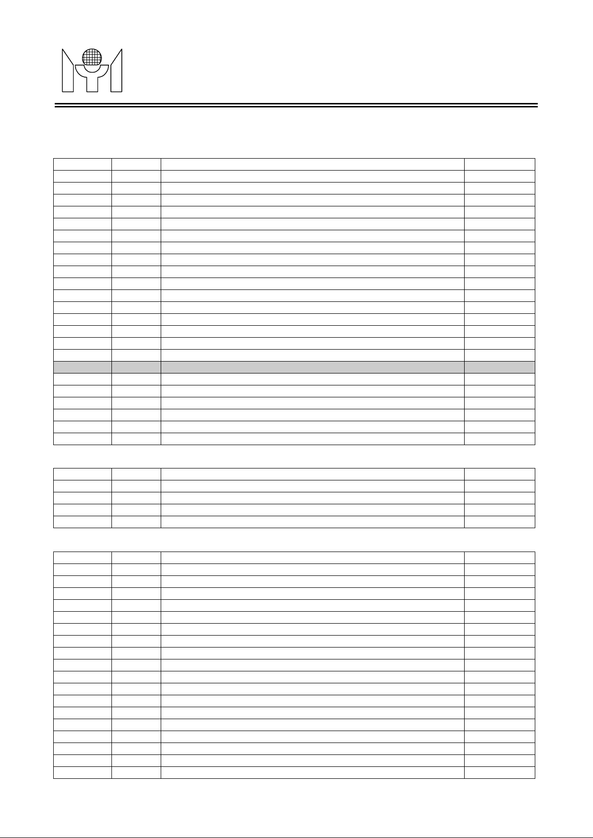
4. REGISTER DESCRIPTION
INPUT CONTROL REGISTERS
Address Mod e Regist ers Reset value
00h R/W Input Image Vertical Active Line Start - Low 20h
01h R/W Input Image Vertical Active Line Start - High 00h
02h R/W Input Image Vertical Active Lines - Low E0h
03h R/W Input Image Vertical Active Lines - High 01h
04h R/W Input Image Horizontal Active Pixel Start - Low 8Bh
05h R/W Input Image Horizontal Active Pixel Start - High 00h
06h R/W Input Image Horizontal Active Pixels - Low 80h
07h R/W Input Image Horizontal Active Pixels - High 02h
10h R/W Input Image Control Register 0 00h
11h R/W Input Image Control Register 1 00h
12h R/W Input Image Control Register 2 00h
13h R/W Input Image Control Register 3 00h
14h R/W Input Image Control Register 4 00h
15h R/W Input Image Control Register 5 00h
16h R/W Input Image Control Register 6 00h
1Ah R/W
1Ch R/W HS1 Sample Window Forward Extend 00h
1Dh R/W HS1 Sample Window Backward Extend 00h
1Fh RO Input Image Status Register 20h R/W Input Image Back Porch Guard Band 00h
21h R/W Input Image Front Porch Guard Band 00h
00h
FRAME SYNC REGISTERS
Address Mod e Regist ers Reset value
2Ch R/W Input Image Vertical Lock Position - Low 22h
2Dh R/W Input Image Vertical Lock Position - High 00h
2Eh R/W Input Image Horizontal Lock Position - Low 00h
2Fh R/W Input Image Horizontal Lock Position - High 00h
Address Mod e Regist ers Reset value
30h R/W Auto Calibration Control 0 80h
31h R/W Auto Calibration Control 1 00h
34h RO
35h RO
36h RO
37h RO
38h RO
39h RO
3Ah RO
3Bh RO
3Ch RO Auto Calibration BLUE Value - Byte 0 3Dh RO Auto Calibration BLUE Value - Byte 1 3Eh RO Auto Calibration BLUE Value - Byte 2 3Fh RO Auto Calibration BLUE Value - Byte 3 -
-
-
-
-
-
-
-
-
40h R/W Pixel Grab V Reference Position - Low 00h
41h R/W Pixel Grab V Reference Position - High 00h
Revision 0.95 - 19 - 2000/06/14
Page 20
MYSON
Input VS Period Count by REFCLK - Low
Input VS Period Count by REFCLK - High
Input V Back Porch Count by Input HS - Low
Input V Back Porch Count by Input HS - High
Input V Total Lines Count by Input HS - Low
Input V Total Lines Count by Input HS - High
Input HS Period Count by REFCLK - Low
Input HS Period Count by REFCLK - High
DISPLAY CONTROL REGISTERS
MTL002
TECHNOLOGY
42h R/W Pixel Grab H Reference Position - Low 00h
43h R/W Pixel Grab H Reference Position - High 00h
44h R/W Histogram Reference Color - RED 00h
45h R/W Histogram Reference Color - GREEN 00h
46h R/W Histogram Reference Color - BLUE 00h
SYNC PROCESSOR REGISTERS
Address Mod e Regist ers Reset value
48h R/W SYNC Processor Control 00h
49h R/W Auto Position Control 00h
4Ah R/W Auto Position Reference Color - RED 00h
4Bh R/W Auto Position Reference Color - GREEN 00h
4Ch R/W Auto Position Reference Color - BLUE 00h
4Eh R/W Clamp Pulse Control 0 00h
4Fh R/W Clamp Pulse Control 1 00h
50h RO
51h RO
52h RO
53h RO
54h RO Input V Active Lines Count by Input HS - Low 55h RO Input V Active Lines Count by Input HS - High 56h RO
57h RO
58h RO
59h RO
5Ah RO Input H Back Porch Count by Input Pixel Clock - Low 5Bh RO Input H Back Porch Count by Input Pixel Clock - High 5Ch RO Input H Active Pixels Count by Input Pixel Clock - Low 5Dh RO Input H Active Pixels Count by Input Pixel Clock - High 5Eh RO Input H Total Pixels Count by Input Pixel Clock - Low 5Fh RO Input H T otal Pixels Count by Input Pixel Clock - High -
(Rev. 0.95)
-
-
-
-
-
-
-
-
Address Mod e Regist ers Reset value
60h R/W Display Vertical Total - Low 48h
61h R/W Display Vertical Total - High 03h
62h R/W Display Vertical SYNC End- Low 05h
63h R/W Display Vertical SYNC End - High 00h
64h R/W Display Vertical Active Start - Low 22h
65h R/W Display Vertical Active Start - High 00h
66h R/W Display Vertical Active End - Low 22h
67h R/W Display Vertical Active End - High 03h
70h R/W Display Horizontal Total - Low 2Bh
71h R/W Display Horizontal Total - High 05h
72h R/W Display Horizontal SYNC End - Low 10h
73h R/W Display Horizontal SYNC End - High 00h
74h R/W Display Horizontal Active Start - Low 27h
75h R/W Display Horizontal Active Start - High 01h
76h R/W Display Horizontal Active End - Low 27h
77h R/W Display Horizontal Active End - High 05h
Revision 0.95 - 20 - 2000/06/14
Page 21
MYSON
Output Clocks Duty Cycle Adjustment
MTL002
TECHNOLOGY
7Fh R/W NFB Timing Control 60h
88h R/W Output Image Control Register 0 01h
89h R/W Output Image Control Register 1 00h
8Ah R/W Output Image Control Register 2 00h
90h R/W Color Gain Control - RED 80h
91h R/W Color Gain Control - GREEN 80h
92h R/W Color Gain Control - BLUE 80h
93h R/W Brightn ess Control - RED 00h
94h R/W Brightness Control - GREEN 00h
95h R/W Brightn ess Control - BLUE 00h
9Fh R/W Gamma Table Data Port A0h R/W OSD Control Register 0 08h
A1h R/W OSD Control Register 1 00h
A4h R/W Output Invert Control 00h
A5h R/W Output Tri-State Control 00h
A6h R/W Output Clocks Delay Adjustment 00h
A7h R/W
A9h R/W Output Miscellaneous Control 00h
AAh R/W Output Vertical Line Number - Low FFh
ABh R/W Output Vertical Line Number - High 02h
ACh RO Output Horizontal Total Pixel Number – Low -
ADh RO Output Horizontal Total Pixel Number – High AEh RO Output Horizontal Total Residue Number – Low AFh RO Output Horizontal Total Residue Number - High -
(Rev. 0.95)
00h
ZOOM CONTROL REGISTERS
Address Mod e Regist ers Reset value
B0h R/W Zoom Control Register 0 66h
B1h R/W Zoom Control Register 1 00h
B4h R/W Zoom Vertical Scale Ratio - Low E0h
B5h R/W Zoom Vertical Scale Ratio - High 9Fh
B6h R/W Zoom Horizontal Scale Ratio - Low E8h
B7h R/W Zoom Horizontal Scale Ratio - High 9Fh
BFh R/W Interpolation Table Data Port -
HOST CONTROL REGISTERS
Address Mod e Regist ers Reset value
C1h R/W Host Control Reg ister 1 00h
CBh RO Host Access Mode Status -
CLOCK CONTROL REGISTERS
Address Mod e Regist ers Reset value
E0h R/W Clock Control Register 00h
E1h WO Clock Synthesizer Value Load -
E2h R/W Clock Synthesizer N Value 0Bh
E3h R/W Clock Synthesizer M Value 32h
E6h R/W Clock Synthesizer R Value 00h
Revision 0.95 - 21 - 2000/06/14
Page 22
MYSON
HS Frequency Change interrupt Compare
Input Image Vertical Act iv e Line Start - Low
It defines the low byte of the start position of the Vertical Active Window.
(Addres s 01h) (R/W)
It defines the high byte of the start position of the Vertical Active W indow.
Inpu t Image Verti c al Act iv e Lines - Low
Input Image Vertical Ac ti v e Lines - High (Add r es s 03h) (R/W)
It defines the low byte of the start position of the Horizontal Active Window.
(Add ress 05h) (R/W)
MTL002
TECHNOLOGY
INTERRUPT CONTROL REGISTERS
Address Mod e Regist ers Reset value
E8h R/W SYNC Interrupt Flag Control 00h
E9h R/W General Interrupt Flag Control 00h
EAh R/W SYNC Interrupt Enable 00h
EBh R/W General Interrupt Enable 00h
ECh R/W
MISCELLANEOUS REGISTERS
Address Mod e Regist ers Reset value
F1h R/W Power Management Control 00h
F4h R/W GPIO Control Register 00h
F5h R/W GPIO Direction Control 00h
F6h R/W GPIO Misc Control 00h
(Add r es s 00h) (R/W)
(Rev. 0.95)
00h
D7-0 IV_ACT_START[7:0]
Input Image Vertic al Act i v e Lin e Start - High
D7-3 Reserved
D2-0 IV_ACT_START[10:8]
(Add ress 02h) (R/W)
It defines the low byte of the number of active lines of the Vertical Active Window.
D7-0 IV_ACT_LEN[7:0]
It defines the high byte of the number of active lines of the Vertical Active Window.
D7-3 Reserved
D2-0 IV_ACT_LEN[10:8]
Inpu t Image Horizon t al Acti v e Pixel Start - Low (Ad dres s 04h) (R/W)
D7-0 IH_ACT_START[7:0]
Input Image Horizon t al Act i v e Pixel Start - High
It defines the high byte of the start position of the Horizontal Active Window.
D7-3 Reserved
Revision 0.95 - 22 - 2000/06/14
Page 23
MYSON
Inpu t Image Horizont al Acti v e Pixels - Low
Inpu t Image Horizon t al Acti v e Pixels - High (A d dres s 07h) (R/W)
(Addres s 10h) (R/W)
1: from Input HREF (only for Video Decoder).
(Addres s 11h) (R/W)
MTL002
TECHNOLOGY
D2-0 IH_ACT_START[10:8]
(Add r es s 06h) (R/W)
It defines the low byte of the number of active pixels of the Horizontal Active Window.
D7-0 IH_ACT_WIDTH[7:0]
It defines the high byte of the number of active pixels of the Horizontal Active Window.
D7-3 Reserved
D2-0 IH_ACT_WIDTH[10:8]
Input Image Contr o l Regist er 0
D7 Horizontal Sampling Point Reference
0: from Input HSYNC.
(Rev. 0.95)
D6 Input YCBCR Format
D5 Digital RGB 6 bit Mode
D4 Digital RGB Mode Select
D3 Input Image Format
D2 Reserved
D1 Input Image Source
D0 ADC Configuration
0: 4-2-2
1: 4-1-1
0: 8 bits
1: 6 bits
0: RGB Input from ADC
1: RGB Input from Panel Link
0: RGB888
1: YCBCR
0: from Graphic source through ADC.
1: from Video source through Video Decoder like SAA7111A.
0: Double Pixel mode
1: Single Pixel mode
Input Image Cont ro l Regist er 1
D7 Reserved
D6-5 Reserved
D4 De-interlace mode Select
0: Spatial Filtering write mode
Revision 0.95 - 23 - 2000/06/14
Page 24

MYSON
(Addres s 12h) (R/W)
Input VSYNC Polarity Source
(Addres s 13h) (R/W)
0: Select Normal HSYNC/ Composite Sync
1: Select Sync On Green
MTL002
TECHNOLOGY
1: Toggle Field write mode
D3-1 Reserved
D0 Reserved
Input Image Cont ro l Regist er 2
D7 Input ODD Field Invert
0: Normal
1: Invert
D6 External Input Interlace Select
0: Non-interlace
1: Interlace
D5 External Input VSYNC Polarity
0: Active Low
1: Active High
D4 External Input HSYNC Polarity
0: Active Low
1: Active High
(Rev. 0.95)
D3 Input ODD Field Source
0: from Internal Detection
1: from External pin.
D2 Input Interlace Source
0: from Internal detection
1: from Register setting (D6)
D1
0: from Internal detection
1: from Register setting (D5)
D0 Input HSYNC Polarity Source
0: from Internal detection
1: from Register setting (D4)
Input Image Cont ro l Regist er 3
D7 Active Position Area for Auto Position in TMDS
0: from Internal Detection
1: from External Data Enable (TDIE)
D6-4 Reserved
D3 Data Enable in TMDS Select
0: from Pin TDIE
1: from Pin RAWHS
D2 Sync On Green Select
D1 Input Vertical Timing based on VSYNC
Revision 0.95 - 24 - 2000/06/14
Page 25

MYSON
(Addres s 14h) (R/W)
(Addres s 15h) (R/W)
(Addres s 16h) (R/W)
MTL002
TECHNOLOGY
0: Leading Edge
1: Trailing Edge
D0 Input Horizontal Timing based on HSYNC
0: Leading Edge
1: Trailing Edge
Input Image Cont ro l Regist er 4
D7 Input ODD Field Detection Point
0: at the start of VSYNC pulse.
1: at the end of VSYNC pulse.
D6 Input Image Port A, B Data and Clocks Swap
0: Normal
1: Swap
D5 Reserved
D4 Input Image CBCR Order Swap
0: Normal
1: Swap
(Rev. 0.95)
D3 Input Image Port A, B V/H SYNC Swap
0: Normal
1: Swap
D2-0 Reserved
Input Image Cont ro l Regist er 5
D7 Horizontal Pixel Valid Select
0: from Internal Programming
1: from External HREF/TDIE
D6-0 Reserved
Input Image Cont ro l Regist er 6
D7 Bit Order in Port B
0: Normal
1: Reverse
D6 Bit Order in Port A
0: Normal
1: Reverse
*D5 Flush Line Buffer Enable
0: Disable
1: Enable
D4 Input Video CREF Signal Invert Enable
0: Normal
1: Invert
D3 Video Clock Selection
0: LLC2
Revision 0.95 - 25 - 2000/06/14
Page 26

MYSON
(Add r es s 1Ah ) (R/W)
Input VSYNC Delay Adjustment
(Add ress 1Ch) (R/W)
Input HS Pulse Width Forward Extend by IDCLK
(Add ress 1Dh) (R/W)
Input HS Pulse Width Backward Extend by IDCLK
HS1BWEXT[7:0]: Used when Interlace First/Second Field Detection.
(Addres s 1Fh) (RO)
Show Display VSYNC signal directly.
MTL002
TECHNOLOGY
1: LLC & CREF
D2 ADC HS Polarity Invert when D1=1
0: Active Low
1: Active High
D1 Raw HS path Enable
0: Disable
1: Enable
D0 Input Image Port Selection in Single Pixel mode
(For Video or Double Pixel mode, this bit has no function.)
0: Port A
1: Port B
Inpu t Delay Contro l 2
D7-4
1111: 15ns gate delay
1110: 14ns gate delay
1101: 13ns gate delay
1100: 12ns gate delay
1011: 3 IDCLKs delay
1010: 2 IDCLKs delay
1001: 1 IDCLK delay
1000: 8ns gate delay
0111: 7ns gate delay
0110: 6ns gate delay
0101: 5ns gate delay
0100: 4ns gate delay
0011: 3ns gate delay
0010: 2ns gate delay
0001: 1ns gate delay
0000: No delay
(Rev. 0.95)
D3-0 Input HSYNC Delay Adjustment
16 steps to change, each of them is 1ns delay/step.
Input HS Pulse Width Forw ard Extend
D7-0
HS1FWEXT[7:0]: Used when Interlace First/Second Field Detection.
Inpu t HS Pulse Width Backw ard Extend
D7-0
Input Image Status Register
D7 Display VSYNC Monitor
D6 Input VSYNC Monitor
D5 External Input Interlace Status
Revision 0.95 - 26 - 2000/06/14
Show Input VSYNC signal directly.
Page 27
MYSON
External Input HSYNC Polarity Status
(Add ress 20h) (R/W)
Input Image Back Porch Guard Band by IDCLK
MTL002
TECHNOLOGY
0: Non-interlace
1: Interlace
D4 Extracted CVSYNC Present Status
0: Not Present
1: Present
D3 External Input VSYNC Present Status
0: Not Present
1: Present
D2 External Input HSYNC Present Status
0: Not Present
1: Present
D1 External Input VSYNC Polarity Status
0: Active Low
1: Active High
D0
0: Active Low
1: Active High
(Rev. 0.95)
Input Image Back Porc h Guard Band
D7-0
HBPGB[7:0]: Used in Auto Position detection to mask out unwanted data.
Inpu t Image Front Porch Guard Band (Ad dres s 21h) (R/W)
D7-0 Input Image Front Porch Guard Band by IDCLK
HFPGB[7:0]: Used in Auto Position detection to mask out unwanted data.
Input Image Vertic al Loc k Posi t io n - Low (Add ress 2Ch) (R/W)
It defines the low byte of the number of input lines where Display image tim ing
synchronizes the input image source.
D7-0 IPV_LOCK_POS[7:0]
Input Image Verti cal Lo c k Posi t i on - High (Addr ess 2Dh) (R/W)
It defines the high byte of the number of input lines where Display image timing
synchronizes the input image source.
D7-3 Reserved
D2-0 IPV_LOCK_POS[10:8]
Input Image Hori zon t al Loc k Posi t i o n - Low (Addr ess 2Eh) (R/W)
It defines the low byte of the number of input pixel clocks where Displa y image
timing synchronizes the input image source.
D7-0 IPH_LOCK_POS[7:0]
Input Image Hori zon t al Loc k Posit i o n - High (Add r ess 2Fh) (R/W)
Revision 0.95 - 27 - 2000/06/14
Page 28

MYSON
Auto Calibr atio n Cont r ol 0 (Address 30h) (R/W)
MYSON proprietary method
Auto Calibration Ready Flag
Auto Calibr atio n Cont r ol 1 (Address 31h) (R/W)
MTL002
TECHNOLOGY
It defines the high byte of the number of input pixel clocks where Display image
timing synchronizes the input image source.
D7-3 Reserved
D2-0 IPH_LOCK_POS[10:8]
D7 Pixel Grab Ready Flag (RO)
0: Ready
1: Not Ready
D6 Pixel Grab Update Enable
0: Stop updating
1: Continue updating
D5 Threshold Select
Used in Histogram mode or MIN/MAX mode.
0: High bound / MAX
1: Low bound / MIN
(Rev. 0.95)
D4 Phase Calibration Method Select
0:
1: Difference Value method
D3-2 Auto Calibration Modes Select
The measured value is available one item at a time,
selected as shown:
00: Phase Calibration Mode
01: Histogram Mode
10: MIN/MAX Mode
11: Pixel Grab Mode
D1 Auto Calibration Burst Mode Enable
(except Pixel Grab Mode)
0: Single Mode
1: Burst Mode
D0 Auto Calibration Enable (W)
(except Pixel Grab Value)
0: Disable
1: Enable
(R)
0: Ready
1: Not Ready
D7-3 Reserved
D2-0 Mask LSBs of Input Image Select
It is used only for Phase Calibration to mask noise.
000: No Mask
001: Mask bit0
010: Mask bit0,1
Revision 0.95 - 28 - 2000/06/14
Page 29
MYSON
MTL002
TECHNOLOGY
011: Mask bit0,1,2
100: Mask bit0,1,2,3
101: Mask bit0,1,2,3,4
110: Mask bit0,1,2,3,4,5
111: Mask bit0,0,1,2,3,4,5,6
Auto Calib ration RED Value - By t e 0 (Addres s 34h) (RO)
It states the byte 0 of the number of Phase Calibration RED value in one frame or
the byte 0 of the number of Histogram Red value in one frame or the Pixel Grab RED
value in one frame of Non_interlace mode or FIRST field of Interlace mode.
D7-0 CALVAL_R[7:0]
Aut o Calib r ation RED Value - Byte 1 (Add ress 35h) (RO)
It states the byte 1 of the number of Phase Calibration RED value in one frame or
the byte 1 of the number of Histogram Red value in one frame or the Pixel Grab GREEN
value in one frame of Non_interlace mode or FIRST field of Interlace mode.
D7-0 CALVAL_R[15:8]
(Rev. 0.95)
Aut o Calib r ation RED Value - Byte 2 (Add ress 36h) (RO)
It states the byte 2 of the number of Phase Calibration RED value in one frame or
the byte 2 of the number of Histogram Red value in one frame or the Pixel Grab BLUE
value in one frame of Non_interlace mode or FIRST field of Interlace mode.
D7-0 CALVAL_R[23:16]
Aut o Calib r ation RED Value - Byte 3 (Add ress 37h) (RO)
It states the byte 3 of the number of Phase Calibration RED value in one frame.
D7-6 Reserved
D5-0 CALVAL_R[29:24]
Aut o Calib rati o n GREEN Valu e - Byte 0 (Addres s 38h) (RO)
It states the byte 0 of the number of Phase Calibration GREEN value in one frame
or the byte 0 of the number of Histogram GREEN value in one frame or
the Pixel Grab RED value in SECOND field of Interlace mode.
D7-0 CALVAL_G[7:0]
Aut o Calib rati o n GREEN Valu e - Byte 1 (Addres s 39h) (RO)
It states the byte 1 of the number of Phase Calibration GREEN value in one frame
or the byte 1 of the number of Histogram GREEN value in one frame or
the Pixel Grab GREEN value in SECOND field of Interlace mode.
D7-0 CALVAL_G[15:8]
Aut o Calib r ation GREEN Value - Byte 2 (Addr ess 3Ah) (RO)
It states the byte 2 of the number of Phase Calibration GREEN value in one frame
Revision 0.95 - 29 - 2000/06/14
Page 30
MYSON
the byte 0 of the number of Histogram BLUE value in one frame or
the byte 1 of the number of Histogram BLUE value in one frame or
the byte 2 of the number of Histogram BLUE value in one frame or
It states the high byte of Vertical Reference Position in Pixel Grab Mode.
MTL002
TECHNOLOGY
or the byte 2 of the number of Histogram GREEN value in one frame or
the Pixel Grab BLUE value in SECOND field of Interlace mode.
D7-0 CALVAL_G[23:16]
Aut o Calib r ation GREEN Value - Byte 3 (Addres s 3Bh ) (RO)
It states the byte 3 of the number of Phase Calibration GREEN value in one frame.
D7-6 Reserved
D5-0 CALVAL_G[29:24]
Auto Calibr ati o n BL UE Value - Byte 0 (Add r ess 3Ch) (RO)
It states the byte 0 of the number of Phase Calibration BLUE value in one frame or
the MIN/MAX RED value in one frame.
D7-0 CALVAL_B[7:0]
Auto Calibr ati o n BL UE Value - Byte 1 (Add r ess 3Dh) (RO)
(Rev. 0.95)
It states the byte 1 of the number of Phase Calibration BLUE value in one frame or
the MIN/MAX GREEN value in one frame.
D7-0 CALVAL_B[15:8]
Auto Calibr ati o n BL UE Value - Byte 2 (Add r ess 3Eh) (RO)
It states the byte 2 of the number of Phase Calibration BLUE value in one frame or
the MIN/MAX BLUE value in one frame.
D7-0 CALVAL_B[23:16]
Auto Calibr ati o n BL UE Value - Byte 3 (Add r ess 3Fh) (RO)
It states the byte 3 of the number of Phase Calibration BLUE value in one frame.
D7-6 Reserved
D5-0 CALVAL_B[29:24]
Pixel Grab V Reference Posit i on - Low (Address 40h) (R/W)
It states the low byte of Vertical Reference Position in Pixel Grab Mode.
D7-0 VGRAB_POS[7:0]
Pixel Grab V Reference Posit i on - High (Address 41h) (R/W)
D7-3 Reserved
Revision 0.95 - 30 - 2000/06/14
Page 31
MYSON
It states the high byte of Horizontal Reference Position in Pixel Grab Mode.
RED (Addr ess 44h) (R/W)
GREEN (Address 45h) (R/W)
BLUE (Add ress 46h) (R/W)
SYNC Process o r Cont rol (Add ress 48h) (R/W)
Auto Posit i o n Cont ro l (Addr ess 49h) (R/W)
Auto Position Ready Flag
MTL002
TECHNOLOGY
D2-0 VGRAB_POS[10:8]
Pixel Grab H Reference Position - Low (Address 42h) (R/W)
It states the low byte of Horizontal Reference Position in Pixel Grab Mode.
D7-0 HGRAB_POS[7:0]
Pixel Grab H Referenc e Positio n - High (Add r ess 43h) (R/W)
D7-3 Reserved
D2-0 HGRAB_POS[10:8]
Histogr am Reference Colo r It states the Histogram Reference RED Color in Histogram Mode.
(Rev. 0.95)
D7-0 HIST_R[7:0]
Histogr am Reference Colo r It states the Histogram Reference GREEN Color in Histogram Mode.
D7-0 HIST_G[7:0]
Histogr am Reference Colo r It states the Histogram Reference BLUE Color in Histogram Mode.
D7-0 HIST_B[7:0]
D7-2 Reserved
D1-0 SYNC Source
00: from H/V SYNC
01: from CVSYNC (Composite SYNC)
1x: Auto switch to CVSYNC when CVSYNC is present, but VSYNC not.
D7-2 Reserved
D1 Auto Position Burst Mode Enable
0: Single Mode
1: Burst Mode
D0 Auto Position Enable (W)
0: Disable
1: Enable
(R)
Revision 0.95 - 31 - 2000/06/14
Page 32
MYSON
0 (Address 4Eh) (R/W)
1 (Address 4Fh) (R/W)
To Adjust Clamp Pulse Width by Input DCLK.
It states the high byte of the number
MTL002
TECHNOLOGY
0: Ready
1: Not Ready
Auto Posi t i o n Reference Color - RED (Ad d r ess 4Ah) (R/W)
It defines the red component color for selecting between black and non-black pixels.
D7-0 REF_COLOR_RED[7:0]
Auto Pos i t i o n Reference Colo r - GREEN (Addr ess 4Bh) (R/W)
It defines the green component color for selecting between black and non-black pixels.
D7-0 REF_COLOR_GREEN[7:0]
Auto Posi t i o n Reference Color - BLUE (Address 4Ch) (R/W)
It defines the blue component color for selecting between black and non-black pixels.
D7-0 REF_COLOR_BLUE[7:0]
Clamp Pulse Contro l
(Rev. 0.95)
D7 Clamp Pulse Mask
D6 Clamp Pulse Start Reference Edge
D5 Clamp Pulse output Polarity
D4-0 Clamp Pulse Start
Clamp Pulse Contro l
D7-5 Reserved
D4-0 Clamp Pulse Width
Input VS Period Count by REFCLK - Low (Add r ess 50h) (RO)
It states the low byte of the number of REFCLK of the Vertical Sync period measurement.
0: Normal
1: Mask out Clamp Pulse
0: From Input HSYNC trailing edge.
1: From Input HSYNC leading edge.
0: Active High
1: Active Low
Start of Clamp Pulse after the selected edge of Input HSYNC by Input DCLK.
D7-0 VSPRD[7:0]
Input VS Period Count by REFCLK - High (Address 51h) (RO)
of REFCLK of the Vertical Sync period measurement.
D7-4 Reserved
Revision 0.95 - 32 - 2000/06/14
Page 33
MYSON
It states the high byte of the number of lines between the end of VSYNC and the acti ve image
Input V Acti ve Image Coun t by Inpu t HS - Low (Add r ess 54h) (RO)
Input V Acti ve Image Coun t by Inpu t HS - High (Add r ess 55h) (RO)
It states the high byte of the number of
MTL002
TECHNOLOGY
D3-0 VSPRD[11:8]
Input V Back Porch Coun t b y Inpu t HS - Low (Add r ess 52h) (RO)
It states the low byte of the number of lines between the end of VSYNC and the active image.
D7-0 VBPW[7:0]
Input V Back Porch Coun t b y Inpu t HS - High (Addr ess 53h) (RO)
D7-3 Reserved
D2-0 VBPW[10:8]
It states the low byte of the number of the active image lines.
D7-0 VACTW[7:0]
(Rev. 0.95)
It states the high byte of the number of the active image lines
D7-3 Reserved
D2-0 VACTW[10:8]
Input V Total Image Coun t b y Input HS - Low (Addr ess 56h) (RO)
It states the low byte of the number of the total image lines.
D7-0 VTOTW[7:0]
Input V Total Image Cou n t b y Inp u t HS - High (Ad d r es s 57h) (RO)
It states the high byte of the number of the total image lines.
D7-3 Reserved
D2-0 VTOTW[10:8]
Input HS Period Cou n t by REFCLK - Low (Add r ess 58h) (RO)
It states the low byte of the number of REFCLKs of the Horizontal Sync period measurement.
D7-0 HSPRD[7:0]
Input HS Period Coun t b y REFCLK - High (Ad d r ess 59h) (RO)
REFCLKs of the Horizontal Sync period measurement.
D7-5 Reserved
D4-0 HSPRD[12:8]
Revision 0.95 - 33 - 2000/06/14
Page 34
MYSON
Input H Back Porch Count by Input Pixel Clock -Low (Addr ess 5Ah) (RO)
It states the high byte of the number of pixels between the end of HSYNC and the active image.
It states the high byte of the number of the Horizontal active image pixels.
It states the high byte of the number of the Horizontal total image pixels.
It defines the high byte of the number of lines per display frame.
MTL002
TECHNOLOGY
It states the low byte of the number of pixels between the end of HSYNC and the active image.
D7-0 HBPW[7:0]
Input H Back Porc h Count by Input Pixel Clock -High (Address 5Bh) (RO)
D7-3 Reserved
D2-0 HBPW[10:8]
Input H Activ e Image Count b y Input Pixel Clock -Low(Add ress 5Ch) (RO)
It states the low byte of the number of the Horizontal active image pixels.
D7-0 HACTW[7:0]
Input H Activ e Image Count b y Input Pixel Clock -High(Ad d r ess 5Dh)(RO)
(Rev. 0.95)
D7-3 Reserved
D2-0 HACTW[10:8]
Input H Total Image Count b y Inpu t Pixel Cloc k- Low (Addr ess 5Eh) (RO)
It states the low byte of the number of the Horizontal total image pixels.
D7-0 HTOTW[7:0]
Input H Total Image Count b y Inpu t Pixel Cloc k- High (Add ress 5Fh) (RO)
D7-3 Reserved
D2-0 HTOTW[10:8]
Display Verti c al Total - Low (Address 60h) (R/W)
It defines the low byte of the number of lines per display frame.
D7-0 DV_TOTAL[7:0]
Display Vertical Total - High (Add r es s 61h) (R/W)
D7-3 Reserved
D2-0 DV_TOTAL[10:8]
Revision 0.95 - 34 - 2000/06/14
Page 35
MYSON
Disp lay Vertical Act iv e Start - Low
It defines the low byte of
Display Verti c al Acti v e Start - High
It defines the high byte of
Disp lay Vertical Acti v e End - Low
It defines the low byte of
Display Verti c al Acti v e End - High (Ad dr ess 67h) (R/W)
It defines the high byte of
(Add ress 71h) (R/W)
MTL002
TECHNOLOGY
Display Verti c al SYNC End - Low (Addres s 62h) (R/W)
It defines the low byte of Vertical SYNC end position in lines.
D7-0 DV_SYNC_END[7:0]
Display Vertic al SYNC End - High (Addr es s 63h) (R/W)
It defines the high byte of Vertical SYNC end position in lines.
D7-3 Reserved
D2-0 DV_SYNC_END[10:8]
Note: Display Vertical SYNC Start is always equal 0.
(Add ress 64h) (R/W)
D7-0 DV_ACT_START[7:0]
Vertical Active region start position in lines.
(Rev. 0.95)
(Add ress 65h) (R/W)
D7-3 Reserved
D2-0 DV_ACT_START[10:8]
D7-0 DV_ACT_END[7:0]
D7-3 Reserved
D2-0 DV_ACT_END[10:8]
Disp lay Horizon t al Total - Low (Add r es s 70h) (R/W)
It defines the low byte of the number of display clock cycles per display line.
Vertical Active region start position in lines.
(Add r es s 66h) (R/W)
Vertical Active region end position in lines.
Vertical Active region end position in lines.
D7-0 DH_TOTAL[7:0]
Display Horizont al Total - High
It defines the high byte of the number of display clock cycles per display line.
D7-3 Reserved
D2-0 DH_TOTAL[10:8]
Revision 0.95 - 35 - 2000/06/14
Page 36
MYSON
(Add ress 73h) (R/W)
Disp lay Horizont al Act iv e Start - Low
It defines the low byte of Horizontal Active region start position in display clock cycles.
Disp lay Horizon t al Acti v e Start - High (Addr es s 75h) (R/W)
It defines the high byte of
Displ ay Horizontal Act i ve End - Low
It defines the low byte of Horizontal Active region end position in display clock cycles.
Disp lay Horizon t al Acti v e End - High (Addres s 77h) (R/W)
It defines the high byte of
(Add ress 88h) (R/W)
MTL002
TECHNOLOGY
Display Horizo nt al SYNC End - Low (Addres s 72h) (R/W)
It defines the low byte of Horizontal SYNC end position in display clock cycles.
D7-0 DH_SYNC_END[7:0]
Display Hori zo n t al SYNC End - High
It defines the high byte of Horizontal SYNC end position in display clock cycles.
D7-3 Reserved
D2-0 DH_SYNC_END[10:8]
Note: Display Horizontal SYNC Start is always equal 0.
D7-0 DH_ACT_START[7:0]
(Add r es s 74h) (R/W)
(Rev. 0.95)
D7-3 Reserved
D2-0 DH_ACT_START[10:8]
D7-0 DH_ACT_END[7:0]
D7-3 Reserved
D2-0 DH_ACT_END[10:8]
NFB Timing Contr ol (Addr ess 7Fh)
It defines the NFB timing setting.
D7-0 Free Running mode Select
60h: Normal
80h: Free Running
Horizontal Active region start position in display clock cycles.
(Add r es s 76h) (R/W)
Horizontal Active region end position in display clock c ycles.
Output Image Contro l Register 0
D7-5 Reserved
Revision 0.95 - 36 - 2000/06/14
Page 37
MYSON
(Add ress 89h) (R/W)
(Add r es s 8Ah ) (R/W)
MTL002
TECHNOLOGY
D4 OUTPUT port MSB / LSB Exchange
0: No Exchange
1: Exchange
D3 Reserved
D2 Output Pixel 18 bit RGB Mode Select
0: 24 bit RGB
1: 18 bit RGB
D1 Output Dual Pixel Data Exchange
0: Normal
1: Exchange
D0 Output Dual Pixel Select
0: Dual Pixel
1: Single Pixel
Output Image Contro l Register 1
D7-6 Reserved
(Rev. 0.95)
D5 RGB Brightness Control Enable
0: Disable
1: Enable
D4 RGB Gain Control Enable
0: Disable
1: Enable
D3-2 Reserved
D1 Border Window Function
0: OFF
1: ON
D0 Output Blank Screen
0: Normal
1: Output Pixel masked as BLACK color
Output Image Contro l Register 2
D7 Reserved
D6 Temporal Dithering Enable
0: Static Dithering
1: Temporal Dithering
D5 Reserved
D4 Dithering Enable
0: Disable
1: Enable
D3-2 Reserved
D1 Gamma Table R/W Access Enable
Revision 0.95 - 37 - 2000/06/14
Page 38
MYSON
Colo r Gain Cont r ol - RED (Addres s 90h) (R/W)
It can be used to adjust the gain of RED component of the Display Image.
(Add ress 91h) (R/W)
It can be used to adjust the gain of GREEN component of the Display Image.
(Addres s 92h) (R/W)
It can be used to adjust the brightness of RED component of the Display Image.
It can be used to adjust the brightness of GREEN component of the Display Image.
Bor d er Win d o w Col o r - RED (Address 96h) (R/W)
When the Display Image is not expanded to full screen, it can be specified as the
Border Wind o w Colo r - GREEN (Address 97h) (R/W)
MTL002
TECHNOLOGY
0: Disable
1: Enable
D0 Gamma Correction Function
0: OFF
1: ON
D7-0 RGAIN[7:0]
0(00h) ~ x1(80h) ~ x1.992185(FFh)
Color Gain Contro l - GREEN
D7-0 GGAIN[7:0]
0(00h) ~ x1(80h) ~ x1.992185(FFh)
Color Gain Contr ol - BLUE
(Rev. 0.95)
It can be used to adjust the gain of BLUE component of the Display Im age.
D7-0 BGAIN[7:0]
0(00h) ~ x1(80h) ~ x1.992185(FFh)
Color Br i gh t n ess Cont r o l - RED (Addr ess 93h) (R/W)
D7-0 RBRIGHT[7:0]
-128(80h) ~ 0(00h) ~127(7Fh)
Color Br i g h t n ess Cont r o l - GREEN (Address 94h) (R/W)
D7-0 GBRIGHT[7:0]
-128(80h) ~ 0(00h) ~127(7Fh)
Color Bri g h t n ess Cont r o l - BLUE (Address 95h) (R/W)
It can be used to adjust the brightness of BLUE component of the Display Image.
D7-0 BBRIGHT[7:0]
-128(80h) ~ 0(00h) ~127(7Fh)
RED component of the border color.
D7-0 BCR[7:0]
Revision 0.95 - 38 - 2000/06/14
Page 39
MYSON
When the Display Image is not expanded to full screen, it can be specified as the
Bor d er Wind o w Color - BLUE (Address 98h) (R/W)
When the Display Image is not expanded to full screen, it can be specified as the
(Add ress 9Fh) (R/W)
OSD Control Regis t er 0 (Addr ess A0h ) (R/W)
0: from Internal Display Dot Clock
1: from Internal Display Dot Clock x 2
OSD Intensity Enable (For MOTOROLA)
(Add r es s A1h ) (R/W)
4 steps to change, each of them is 1ns delay/step.
MTL002
TECHNOLOGY
GREEN component of the border color.
D7-0 BCG[7:0]
BLUE component of the border color.
D7-0 BCB[7:0]
Gamma Table Data Port
Since the Gamma Table is downloadable, this data port is the entry address.
D7-0 GAMMA_PORT[7:0]
D7 OSD Output Clock Select
(Rev. 0.95)
D6-4 Reserved
D3 OSD Function
D2
D1-0 OSD TYPE Select
OSD Contro l Regist er 1
D7 OSD Output HS Invert
D6 OSD Output DCLK Invert
0: OFF
1: ON
0: Disable
1: Enable
00: OSDRGB = {R0000000, G0000000, B0000000}
01: OSDRGB = {RR000000, GG000000, BB000000}
10: OSDRGB = {RRRR0000, GGGG0000, BBBB0000}
11: OSDRGB = {RRRRRRRR, GGGGGGGG, BBBBBBBB}
R = OSDR, G = OSDG, B = OSDB
0: Normal
1: Invert.
0: Normal
1: Invert.
D5-4 OSD Output HS Delay
D3 OSD Input Data Sample Clock Invert
Revision 0.95 - 39 - 2000/06/14
0: Normal.
Page 40

MYSON
8 steps to change, each of them is 1ns delay/step.
(Addr es s A4h ) (R/W)
(Add r es s A5h ) (R/W)
MTL002
TECHNOLOGY
1: Invert.
D2-0 OSD Input Data Sample Clock Delay
Output Invert Contro l
D7 Reserved
D6 RGB Data Invert Enable
D5 Display DHCLK Invert
D4 Display DCLK Invert
D3 Reserved
0: Disable
1: Enable
0: Normal
1: Invert
0: Normal
1: Invert
(Rev. 0.95)
D2 Display Data Enable (DDEN) Invert
0: Normal
1: Invert
D1 Display VSYNC Invert
0: Normal
1: Invert
D0 Display HSYNC Invert
0: Normal
1: Invert
Output Tri_state Control
D7 Display Data R2OUT, G2OUT, B2OUT Output Disable
0: Normal
1: Tri_stated
D6 Display Data R1OUT, G1OUT, B1OUT Output Disable
0: Normal
1: Tri_stated
D5 Display DHCLK Output Disable
0: Normal
1: Tri_stated
D4 Display DCLK Output Disable
0: Normal
1: Tri_stated
D3 OSD OCLK / OVSYNC / OHSYNC Output Disable
0: Normal
1: Tri_stated
Revision 0.95 - 40 - 2000/06/14
Page 41

MYSON
Display DHCLK delay adjustment
Display DCLK delay adjustment
Output Clocks Duty Cycle Adjust ment (Ad dress A7h) (R/W)
Display DHCLK duty cycle Increas
Display DHCLK duty cycle adjustment
Display DCLK duty cycle Increase/Decrease
Display DCLK duty cycle adjustment
(Add r es s A9h) (R/W)
MTL002
TECHNOLOGY
D2 Display Data Enable (DDEN) Output Disable
0: Normal
1: Tri_stated
D1 Display VSYNC Output Disable
0: Normal
1: Tri_stated
D0 Display HSYNC Output Disable
0: Normal
1: Tri_stated
Outpu t Clock s Delay Adjus tm ent (Add ress A6h) (R/W)
D7-4
16 steps to adjust, Typical 1ns delay/step
D3-0
16 steps to adjust, Typical 1ns delay/step
(Rev. 0.95)
D7
0: Decrease
1: Increase
D6-4
8 steps to adjust, Typical 0.5ns delay/step
D3
0: Decrease
1: Increase
D2-0
8 steps to adjust, Typical 0.5ns delay/step
Outpu t Miscellaneous Contr ol
D7 Second field Line Buffer Overflow status for Interlace input (RO)
0: Not Overflow
1: Overflow
D6 Second field Line Buffer Underflow status for Interlace input (RO)
0: Not Underflow
1: Underflow
D5 First field Line Buffer Overflow status for Interlace input or
Line buffer Overflow status for Non-interlace input (RO)
0: Not Overflow
1: Overflow
e/Decrease
D4 First field Line Buffer Underflow status for Interlace input or
Line Buffer Overflow status for Non-interlace input (RO)
0: Not Underflow
1: Underflow
D3 Auto Output Horizontal Total Calculation Start (W)
Revision 0.95 - 41 - 2000/06/14
Page 42
MYSON
Auto Output Horizontal Total Calculation Ready Flag
Output Vertical Activ e Line Number - Low
AAh) (R/W)
It defines the low byte of Output Vertical Active Line Number only used for getting the values of
Output Vertical Acti v e Line Number - High
ABh) (R/W)
It states the high byte of Output Horizontal Total Pixel Residue Number.
Zoom Cont r o l Register 0 (Address B0h) (R/W)
MTL002
TECHNOLOGY
0: Disable
1: Enable
(R)
0: Ready
1: Not Ready
D2-0 Reserved
(Address
Reg. ACh and ADh.
D7-0 OVDE[7:0]
It defines the high byte of Output Vertical Active Line Number only used for getting the values of
Reg. ACh and ADh.
D1-0 OVDE[9:8]
(Address
(Rev. 0.95)
Output Horizon t al Total Pixel Number - Low (Address ACh ) (RO)
It states the low byte of Output Horizontal Total Pixel Number.
D7-0 OHTOT[7:0]
Output Horizont al Total Pixel Numb er - High (Address ADh) (RO)
It states the high byte of Output Horizontal Total Pixel Number.
D2-0 OHTOT[10:8]
Output Horizon t al Total Residu e Numb er - Low (Address AEh) (RO)
It states the low byte of Output Horizontal Total Pixel Residue Number.
D7-0 OHTOT_RES[7:0]
Output Horizont al Total Resid ue Number - High (Ad dress AFh) (RO)
D1-0 OHTOT_RES[9:8]
D7 Reserved
D6-4 Vertical Scale Select
0XX: PASS mode
10X: DUPLICATE mode
110: BILINEAR mode
111: INTERPOLATION TABLE mode
D3 Reserved
Revision 0.95 - 42 - 2000/06/14
Page 43
MYSON
Zoom Contr o l Regist er 1 (Address B 1h) (R/W)
Interpolation Table R/W Access Enable
It defines the low byte of vertical scale ratio value for scale up.
(Add r es s B5h ) (R/W)
It defines the low byte of vertical scale ratio value for scale up.
] for Extension Boundary Scale mode
It defines the low byte of horizontal scale ratio value for scale up.
(Add r es s B7h ) (R/W)
It defines the high byte of horizontal scale ratio value for scale up.
It defines the entry address of the Interpolation table data port.
MTL002
TECHNOLOGY
D2-0 Horizontal Scale Select
0xx: PASS mode
10x: DUPLICATE mode
110: BILINEAR mode
111: INTERPOLATION TABLE mode
D7-1 Reserved
*D3 Horizontal Zoom Factor mode
0: Uniform Scale mode
1: Extension Boundary Scale mode
*D2 Vertical Zoom Factor mode
0: Uniform Scale mode
1: Extension Boundary Scale mode
D0
0: Disable
1: Enable
(Rev. 0.95)
Zoom Vertic al Scale Ratio – Low (Add ress B4h) (R/W)
D7-0 ZVSF[7:0]
Zoom Vertic al Scale Ratio - High
D7-0 ZVSF[15:8]
ZVSF = CEIL[(input_height – 1) / (output_height – 1) *216] for Uniform Scale mode
ZVSF = CEIL[(input_height / output_height) *2
Zoom Horizon t al Scale Ratio - Low (Add r ess B6h) (R/W)
D7-0 ZHSF[7:0]
Zoom Horizo nt al Scale Ratio - High
D7-0 ZHSF[15:8]
16
ZHSF = CEIL[(input_width – 1) / (output_width – 1) *216] for Uniform Scale mode
ZHSF = CEIL[(input_width / output_width) *216] for Extension Boundary Scale mode
Interpolati o n Table Data Port (Address BFh) (R/W)
Revision 0.95 - 43 - 2000/06/14
Page 44
MYSON
Host Cont ro l Regis t er 1 (Addr ess C1h) (R/W)
1: Delay to Display VSYNC
Host Acc ess Mode Status (Address
(Add ress E0h) (R/W)
40h: Internal Display Clock (PLL)
A5h: External Display Clock 2
(Add r es s E1h) (WO)
(Add ress E3h) (R/W)
Clock Syn t hesizer R Valu e (Address E6h) (R/W)
MTL002
TECHNOLOGY
D7-0 TFPORT[7:0]
D7 Reserved
D6 I2C Bus Address No Increment
0: Normal
1: No Increment
D5 Double Buffer load Select
0: Immediately
D4 Registers Double Buffer function Enable
D3-2 Reserved
D1 Display Registers Double Buffer Load (WO)
0: Disable
1: Enable
(Rev. 0.95)
D0 Input Registers Double Buffer Load (WO)
CBh ) (RO)
D7-2 Reserved
D1-0 Host Access Mode
0x: 3-wire Serial mode
10: 2-wire Serial mode (IIC)
11: 8-bit Parallel mode
Clock Synthesizer Control Regist er
D7-0 Display Clock Selection
Note: Reg. F1h/D3 must be 1.
25h: External Display Clock 1
Clock Synth esizer Value Load
D7-1 Reserved
D0 Display Clock Synthesizer Value Load (WO)
Display Cloc k Syn t h esi zer N Value (Add r ess E2h) (R/W)
D7-0 Display Clock Synthesizer N value
Display Cloc k Synth esizer M Value
D7-0 Display Clock Synthesizer M value
Revision 0.95 - 44 - 2000/06/14
Page 45

MYSON
Display VSYNC pulse detected
1: Any Display VSYNC pulse detected
VSYNC Polarity Change Status
HSYNC Polarity Change Status
HSYNC Frequency Change
MTL002
TECHNOLOGY
D7 Reserved
D6-4 REFCLK Clock Divider value
000: No divided
001: Divided by 2
010: Divided by 4
011: Divided by 8
100: Divided by 3
101: Divided by 6
110: Divided by 12
111: Divided by 24
D3-2 Reserved
D1-0 Display Clock Synthesizer R value
00: No divided
01: Divided by 2
1x: Divided by 4
SYNC Interru p t Flag Cont r o l (Add r es s E8h) (R)
It contains the status of SYNC Interrupts.
(Rev. 0.95)
D7 Display VSYNC Pulse Interrupt Status
0: No
D6 Input VSYNC Pulse Interrupt Status
D5 VSYNC Presence Change Status
D4 HSYNC Presence Change Status
D3
D2
D1 VSYNC Frequency Change Status
0: No Input VSYNC pulse detected
1: Any Input VSYNC pulse detected
0: No Change
1: Change
0: No Change
1: Change
0: No Change
1: Change
0: No Change
1: Change
0: No Change
1: Change
D0
0: No Change
1: Change
SYNC Interr u p t Flag Contr o l (Add r ess E8h) (W)
Revision 0.95 - 45 - 2000/06/14
Status
Page 46
MYSON
Clear HSYNC Frequency Change Interru
General Interr up t Flag Contr o l (Add res s E9h) (R)
Auto Position Finish Status (valid for Single mode only)
Auto Calibration Finish Status (valid for Single mode only)
General Interru p t Flag Contro l (Add ress E9h) (W)
MTL002
TECHNOLOGY
It is used to clear the corresponding SYNC interrupt signal when Software finishes
serving the interrupt service routine.
D7 Clear Display VSYNC Pulse Interrupt Enable
0: Disable
1: Enable
D6 Clear Input VSYNC Pulse Interrupt Enable
0: Disable
1: Enable
D5 Clear VSYNC Presence Change Interrupt Enable
0: Disable
1: Enable
D4 Clear HSYNC Presence Change Interrupt Enable
0: Disable
1: Enable
D3 Clear VSYNC Polarity Change Interrupt Enable
0: Disable
1: Enable
(Rev. 0.95)
D2 Clear HSYNC Polarity Change Interrupt Enable
0: Disable
1: Enable
D1 Clear VSYNC Frequency Change Interrupt Enable
0: Disable
1: Enable
D0
0: Disable
1: Enable
It contains the status of General Interrupts.
D7-3 Reserved
D2 Reserved
D1
0: Not Finish
1: Finish
D0
0: Not Finish
1: Finish
pt Enable
It is used to clear the corresponding general interrupt signal when Software finishes
serving the interrupt service routine.
D7-3 Reserved
Revision 0.95 - 46 - 2000/06/14
Page 47
MYSON
VSYNC Polarity Change Interrupt Enable
HSYNC Polarity Change Interrupt Enable
HSYNC Frequency Change Interrupt Enable
General Interru p t Flag Enable (Add ress
MTL002
TECHNOLOGY
D2 Reserved
D1 Clear Auto Position Finish Interrupt Enable
0: Disable
1: Enable
D0 Clear Auto Calibration Finish Interrupt Enable
0: Disable
1: Enable
SYNC Interr u p t Flag Enable (Address EAh) (R/W)
It is used to enable SYNC Interrupt function.
D7 Display VSYNC Pulse Interrupt Enable
0: Disable
1: Enable
D6 Input VSYNC Pulse Interrupt Enable
0: Disable
1: Enable
(Rev. 0.95)
D5 VSYNC Presence Change Interrupt Enable
0: Disable
1: Enable
D4 HSYNC Presence Change Interrupt Enable
0: Disable
1: Enable
D3
0: Disable
1: Enable
D2
0: Disable
1: Enable
D1 VSYNC Frequency Change Interrupt Enable
0: Disable
1: Enable
D0
0: Disable
1: Enable
EBh ) (R/W)
It is used to enable General Interrupt functions.
D7-3 Reserved
D2 Reserved
D1 Auto Position Finish Interrupt Enable
0: Disable
Revision 0.95 - 47 - 2000/06/14
Page 48
MYSON
HS Frequenc y Change Interrup t Comp are (Address
It is used to control Interrupt generation by comparing the frequency change value
GPIO Cont r ol Regis ter (Add ress F4h) (R/W)
MTL002
TECHNOLOGY
1: Enable
D0 Auto Calibration Finish Interrupt Enable
0: Disable
1: Enable
ECh) (R/W)
when Input HS Frequency Changes.
D7-0 HSCMPREG[7:0]
Power Management Cont r o l (Add r ess F1h) (R/W)
D7 Reserved
D6 Power Down Gamma & Interpolation Table
0: Normal
1: Power Down
D5 Reserved
(Rev. 0.95)
D4 Power Down Line Buffers
0: Normal
1: Power Down
D3 Power Down Oscillator PAD
0: Power Down
1: Normal
D2 Reserved
D1 Power Down all the clocks except REFCLK
0: Normal
1: Power Down
D0 Software Reset Enable
0: Disable
1: Enable
It controls the data of the GPIO pins.
D7-4 Reserved
D3-0 GPIO[3:0]
GPIO Direct i o n Cont r o l (Add r ess F5h) (R/W)
It controls the In/Out direction of the GPIO pins, where “0” means Input, and
“1” means Output.
D7-4 Reserved
D3-0 GPIO[3:0] In/Out Select
Revision 0.95 - 48 - 2000/06/14
Page 49

MYSON
Misc Cont r o l (Add r ess F6h) (R/W)
MTL002
TECHNOLOGY
0: Input
1: Output
GPIO
It defines the GPIO pins miscellaneous control.
D7-1 Reserved
D0 GPIO[1:0] Output Pins Source
0: from Reg. F4h GPIO[1:0]
1: from ADVS/ADHS
(Rev. 0.95)
Revision 0.95 - 49 - 2000/06/14
Page 50
MYSON
5. ELECTRICAL CHA R ACTERISTICS
5.1 DC CHARACTERISTICS
PAR AMETER
MTL002
TECHNOLOGY
Table 5.1 Recommended Operating Conditio ns
SYMBOL
Vcc Operation Voltage 3.0 3.3 3.6 V
Tamb Operating Ambient Temperature 0 70
Tstg Storage Temperature -55 150
SYMBOL PARAMETER CONDITIONS MIN TYP MAX UNIT
VIL Input Low Voltage 0.8 V
VIH Input High Voltage 2.0 V
Vt- Input Schmitt Trigger
Vt+ Input Schmitt Trigger
VOL Output Low Voltage 0.4 V
VOH Output High Voltage 2.4 V
RI Input Pull-up/Down
ILI Input Leakage Current -10 10 uA
ILO Output Le akage Current -20 20 uA
Table 5.2 DC Electric al Characteris t ic s fo r 3.3 V Operation
Low Voltage at pins
SDA and SCK
High Voltage at pins
SDA and SCK
VIL = 0v or
Resistance
VIH = VCC
MIN TYP MAX UNIT
1.0
1.7
75 Kohm
(Rev. 0.95)
o
C
o
C
Revision 0.95 - 50 - 2000/06/14
Page 51
MYSON
5.2 AC CHARA CTERISTICS
PARAMETER
MTL002
TECHNOLOGY
¨ Input Interface Timin g
Figur e 5.2.1 Input Interface Timing
IPCLK
Input VS/HS
PIXIN[23:0]
(Rev. 0.95)
TivhhTivhs
Tids
Tidh
Table 5.2.1 Input Interface Timing
SYMBOL
Tids Input Image Signal Setup Time for IPCLK 2 ns
Tidh Input Image Signal Hold Time for IPCLK 3 ns
Tivhs Input VSYNC/HSYNC Setup Time for IPCLK 2 ns
Tivhh Input VSYNC/HSYNC Hold Time for IPCLK 3 ns
MIN MAX UNIT
Revision 0.95 - 51 - 2000/06/14
Page 52
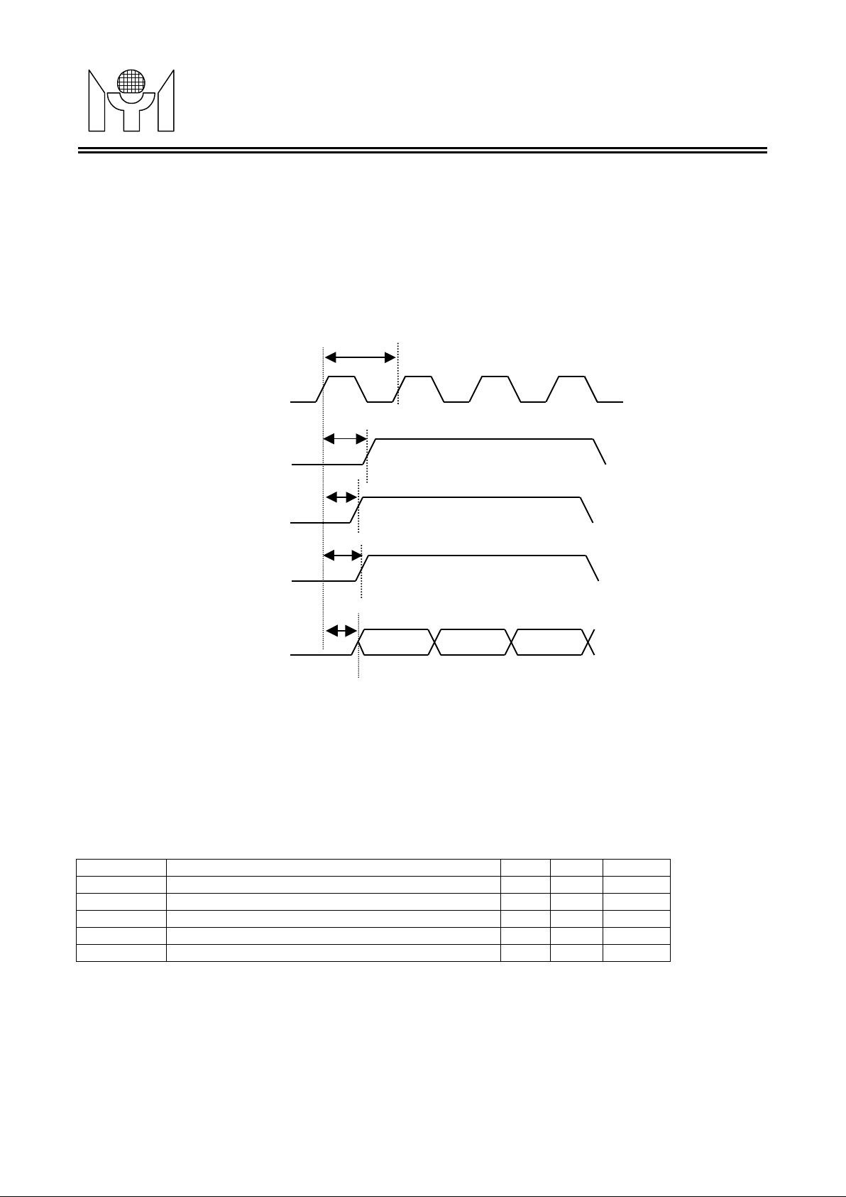
MYSON
PARAMETER
Display VSYNC Output Delay to DDCLK
Display HSYNC Output Delay to DDCLK
Display DDEN Output Delay to DDCLK
Display Data Output Delay to DDCLK
MTL002
TECHNOLOGY
¨ Output Interface Timing
Figur e 5.2.2 Outpu t Interface Timing
DDCLK
Display VS
Display HS
(Rev. 0.95)
Tdck
Tdvs
Tdhs
Tdde
Display DDEN
Tddp
PIXOUT1[23:0] / PIXOUT2[23:0]
Table 5.2.2 Output Interface Timing
SYMBOL
Tdck Display Clock DDCLK Frequency 10 ns
Tdvs
Tdhs
Tdde
Tddp
Note: DDCLK phase can be adjusted relative to data and control outputs using the DDCLK_INV
(Reg. A4h/D5-4) and DDCLK_DELAY[2:0] (Reg. A6h/D7-0) programming controls.
MIN MAX UNIT
2 ns
0.5 ns
1 ns
1.5 ns
Revision 0.95 - 52 - 2000/06/14
Page 53
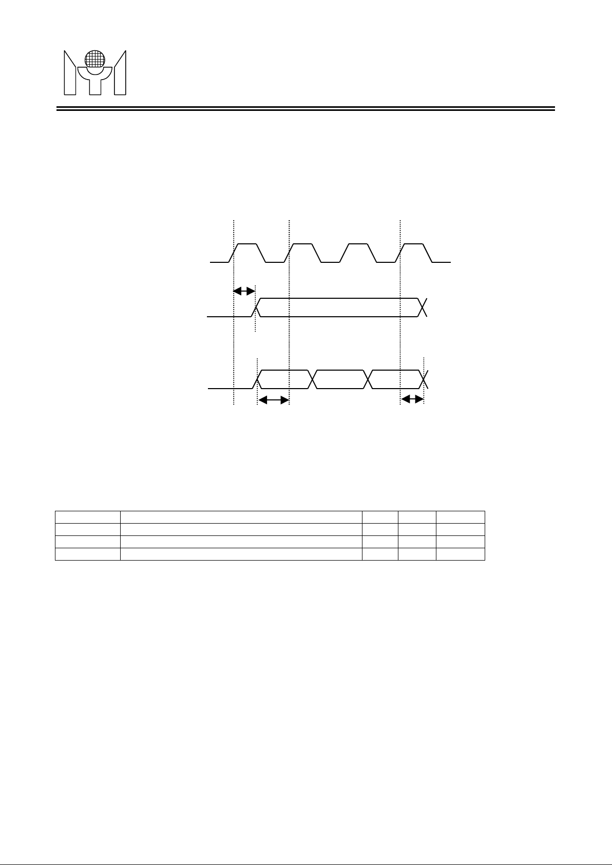
MYSON
PARAMETER
OSD VS / HS Output Delay to OCLK
MTL002
TECHNOLOGY
¨ OSD Int erf ace Timin g
Figur e 5.2.3 OSD Interface Timin g
OCLK
OVSYNC / OHSYNC
Input OSDDEN / OSDRED /
OSDGRN / OSDBLU
(Rev. 0.95)
Tosdd
Tosds Tosdh
Table 5.2.3 OSD Interf ace Timin g
SYMBOL
Tosdd
Tosds OSD Signal Input Setup Time for OCLK 5.5 ns
Tosdh OSD Signal Input Hold Time for OCLK 0 ns
Note: OCLK phase can be adjusted using OCLK_INV (Reg. A1h/D3) programming control and OHSYNC
phase can be adjusted using OHSYNC_DELAY[1:0] (Reg. A1h/D5-4) programming control.
MIN MAX UNIT
2 ns
Revision 0.95 - 53 - 2000/06/14
Page 54
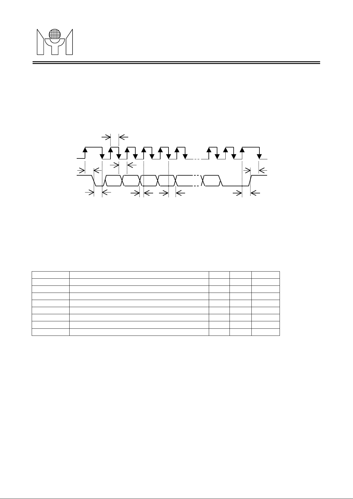
MYSON
PARAMETER
MTL002
TECHNOLOGY
¨ I2C Hos t Interf ace Timin g
Figur e 5.2.4 I2C Host Interface Timin g
Thigh
Tsu:sta Thd:sto
Thd:sta
Tlow
Tsu:dat
Thd:dat
(Rev. 0.95)
Tsu:sto
Table 5.2.4 I2C Host Interface Timin g
SYMBOL
Thigh Clock High Period 500 ns
Tlow Clock Low Period 500 ns
Tsu:dat Data in Setup Time 200 ns
Thd:dat Data in Hold Time 100 ns
Tsu:sta Start condition Setup Time 500 ns
Thd:sta Start condition Hold Time 500 ns
Tsu:sto Stop condition Setup Time 500 ns
Thd:sto Stop condition Hold Time 500 ns
MIN MAX UNIT
Revision 0.95 - 54 - 2000/06/14
Page 55
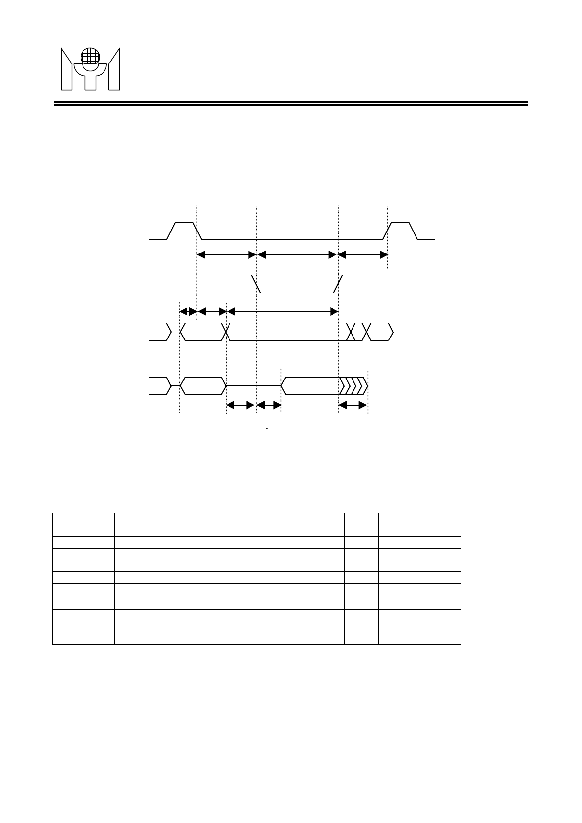
MYSON
PARAMETER
WR/RD Pulse Width
ALE Low to WR/RD Low
WR/RD High to ALE High
WR/RD
MTL002
TECHNOLOGY
¨ 8-bit Direct Host Interface Timi ng
Figur e 5.2.5 8-bit Direct Host Interface Timing
ALE
Tllwl Trwpw
Tavll Tllax
AD(7:0)/WR
A0-A7
(Rev. 0.95)
Twhlh
Tqvwh
DATA IN
AD(7:0)/RD
Trlaz
Table 5.2.5 8-bit Direct Host Interface Timing
SYMBOL
Tavll Addr ess Valid to ALE Low 3 ns
Tllax Address Hold After A LE Low 5 ns
Trwpw
Tllwl
Tqvwh Data Valid to WR High 3 ns
Twhqx Data Hold After WR 10 ns
Twhlh
Trlaz RD Low to Ad dress Float -5 ns
Trldv RD Low to Valid Data In 30 ns
Trhdz Data Float after RD High 0 15 ns
– Register IO R/W 0 ns
DATA OUTA0-A7
TrhdzTrldv
MIN MAX UNIT
35 ns
5 ns
Revision 0.95 - 55 - 2000/06/14
Page 56
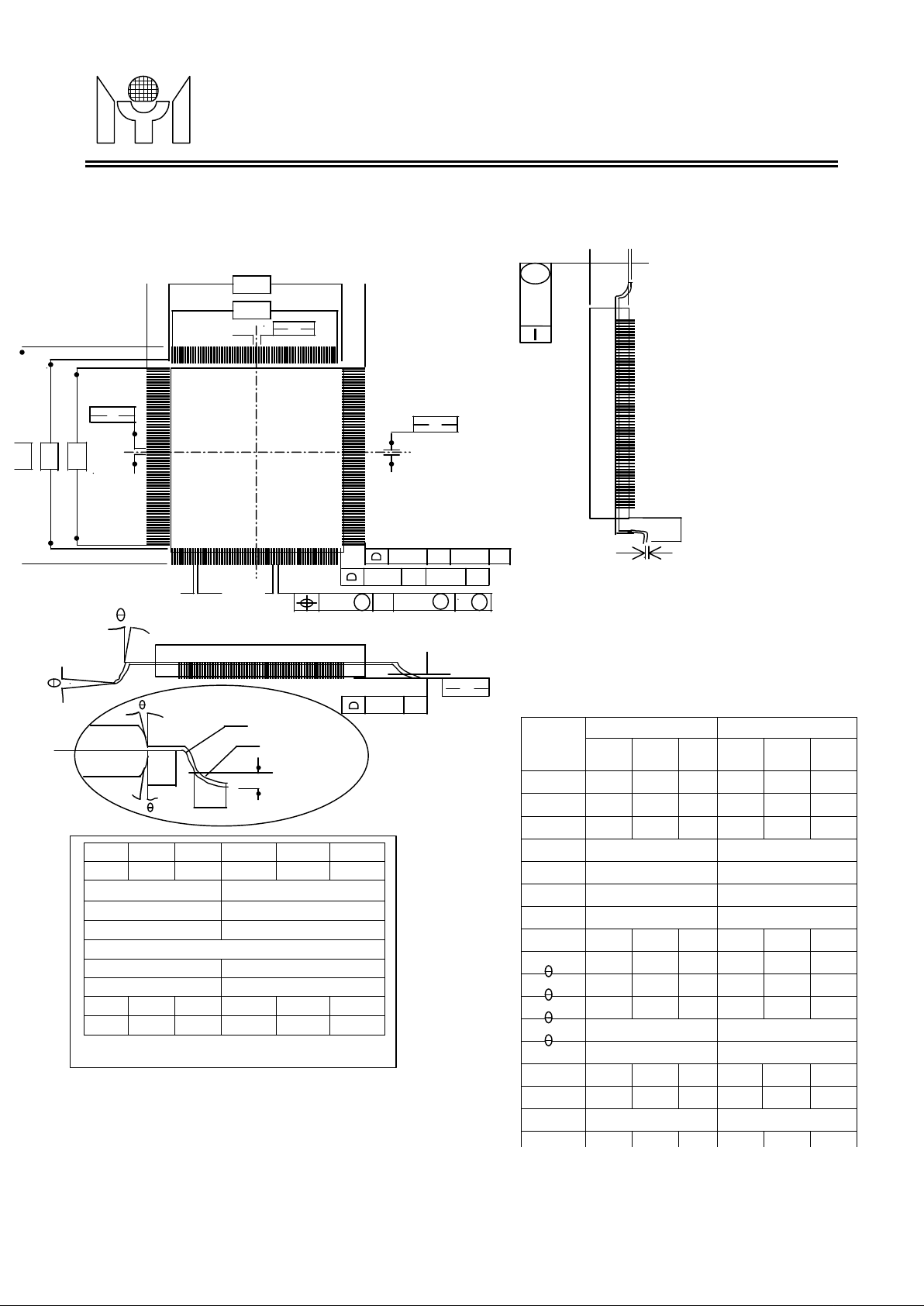
MYSON
6. PACKAGE DIMENSION
3
D
A-B
b
A-B D
A-B D
e
E1
E2
D1
0.05
;L1
B
A
S
S
L
0.25mm
MTL002
TECHNOLOGY
120/128/132/144/160/184/208/256L OFP
28 X 28 X 3.32 mm
2.6mm FOOTPRINT
1
D2
D
4X
ddd
4X
bbb
C
aaa
(Rev. 0.95)
A2
C
H
S
A1
C
C
2
R1
R2
GAGE PLANE
ccc
C
MIN. NOM. MAX. MIN. NOM. MAX.
0.17 0.20 0.27 0.007 0.008 0.011
0.50 BSC. 0.020 BSC.
25.50 1.004
25.50 1.004
TOLERANCES OF FORM AND POSITION
0.20 0.008
0.20 0.008
X 0.08 X X 0.003 X
X 0.08 X X 0.003 X
NOTES:
1. DIMENSIONS D1 AND E1 DO NOT INCLUDE MOLD PROTRUSION.
2. SIMENSION b DOES NOT INCLUDE DAMBAR PROTRUSION.
ALLOWABLE DAMBAR PROTRUSION SHALL NOT CAUSE THE
LEAD WIDTH TO EXCEED THE MAXIMUM b DIMENSION BY MORE
THAN 0.08mm.
DAMBAR CAN NOT BE LOCATED ON THE LOWER RADIUS OR THE
FOOT. THE MINIMUM SPACE BETWEEN PROTRUSION AND AN
ADJACENT LEAD SHALL NOT BE LESS THAN 0.07 mm.
3. THE TOP PACKAGE BOOY SIZE MAY BE SMALLER THAN THE
BOTTOM PACKAGE BOOY SIZE.
SEATING PLANE
SYMBOL
A1 0.25 X X 0.010 X X
A2 3.20 3.32 3.60 0.126 0.131 0.142
D1 28.00 BSC 1.102 BSC
E1 28.00 BSC 1.102 BSC
R2 0.08 X 0.25 0.003 X 0.010
R1 0.08 X X 0.003 X X
1 0° X X 0° X X
2 8° REF 8° REF
3 8° REF 8° REF
L1 1.30 0.051 REF
MIN. NOM.
A X X 4.10 X X 0.161
D 30.60 BSC 1.205 BSC
E 30.60 BSC 1.205 BSC
C 0.09 0.15 0.20 0.004 0.005 0.008
L 0.45 0.60 0.75 0.018 0.024 0.030
MILLIMETER INCH
MAX
MIN. NOM. MAX.
.
0° 3.5° 7° 0° 3.5° 7°
Revision 0.95 - 56 - 2000/06/14
 Loading...