

Page 1
1
Motorola TMOS Power MOSFET Transistor Device Data
N–Channel Enhancement–Mode Silicon Gate
This TMOS Power FET is designed for high speed, low loss
power switching applications such as switching regulators, converters, solenoid and relay drivers.
• Silicon Gate for Fast Switching Speeds
• Low R
DS(on)
— 0.3 Ω Max
• Rugged — SOA is Power Dissipation Limited
• Source–to–Drain Diode Characterized for Use With
Inductive Loads
• Low Drive Requirement — V
GS(th)
= 4.0 V Max
• Surface Mount Package on 16 mm Tape
MAXIMUM RATINGS
Rating Symbol Value Unit
Drain–Source Voltage V
DSS
150 Vdc
Drain–Gate Voltage (RGS = 1.0 MΩ) V
DGR
150 Vdc
Gate–Source Voltage — Continuous
Gate–Source Voltage — Non–Repetitive (tp ≤ 50 µs)
V
GS
V
GSM
± 20
± 40
Vdc
Vpk
Drain Current — Continuous
Drain Current — Pulsed
I
D
I
DM
6.0
20
Adc
Total Power Dissipation @ TC = 25°C
Derate above 25°C
P
D
20
0.16
Watts
W/°C
Total Power Dissipation @ TA = 25°C
Derate above 25°C
P
D
1.25
0.01
Watts
W/°C
Total Power Dissipation @ TA = 25°C (1)
Derate above 25°C
P
D
1.75
0.014
Watts
W/°C
Operating and Storage Junction Temperature Range TJ, T
stg
–65 to +150 °C
THERMAL CHARACTERISTICS
Thermal Resistance — Junction to Case
Thermal Resistance — Junction to Ambient
Thermal Resistance — Junction to Ambient (1)
R
θJC
R
θJA
R
θJA
6.25
100
71.4
°C/W
ELECTRICAL CHARACTERISTICS (T
J
= 25°C unless otherwise noted)
Characteristic
Symbol Min Max Unit
OFF CHARACTERISTICS
Drain–Source Breakdown Voltage
(VGS = 0 Vdc, ID = 0.25 mAdc)
V
(BR)DSS
150 — Vdc
Zero Gate Voltage Drain Current
(VDS = Rated V
DSS
, VGS = 0 Vdc)
TJ = 125°C
I
DSS
—
—
10
100
µAdc
(1) These ratings are applicable when surface mounted on the minimum pad size recommended. (continued)
Designer’s Data for “Worst Case” Conditions — The Designer’s Data Sheet permits the design of most circuits entirely from the information presented. SOA Limit
curves — representing boundaries on device characteristics—are given to facilitate “worst case” design.
Designer’s is a trademark of Motorola, Inc. TMOS is a registered trademark of Motorola, Inc.
Order this document
by MTD6N15/D
SEMICONDUCTOR TECHNICAL DATA
CASE 369A–13, Style 2
DPAK (TO–252)
TMOS POWER FET
6.0 AMPERES
150 VOLTS
R
DS(on)
= 0.3 OHM
D
S
G
Motorola, Inc. 1996
Page 2

MTD6N15
2
Motorola TMOS Power MOSFET Transistor Device Data
ELECTRICAL CHARACTERISTICS — continued
(T
J
= 25°C unless otherwise noted)
Characteristic
Symbol Min Max Unit
OFF CHARACTERISTICS — continued
Gate–Body Leakage Current, Forward (V
GSF
= 20 Vdc, VDS = 0) I
GSSF
— 100 nAdc
Gate–Body Leakage Current, Reverse (V
GSR
= 20 Vdc, VDS = 0) I
GSSR
— 100 nAdc
ON CHARACTERISTICS*
Gate Threshold Voltage (VDS = VGS, ID = 1.0 mAdc)
TJ = 100°C
V
GS(th)
2.0
1.5
4.5
4.0
Vdc
Static Drain–Source On–Resistance (VGS = 10 Vdc, ID = 3.0 Adc) R
DS(on)
— 0.3 Ohm
Drain–Source On–Voltage (VGS = 10 Vdc)
(ID = 6.0 Adc)
(ID = 3.0 Adc, TJ = 100°C)
V
DS(on)
—
—
1.8
1.5
Vdc
Forward Transconductance (VDS = 15 Vdc, ID = 3.0 Adc) g
FS
2.5 — mhos
DYNAMIC CHARACTERISTICS
Input Capacitance
C
iss
— 1200 pF
Output Capacitance
(VDS = 25 Vdc, VGS = 0 Vdc,
f = 1.0 MHz)
C
oss
— 500
Reverse Transfer Capacitance
See Figure 11
C
rss
— 120
SWITCHING CHARACTERISTICS* (TJ = 100°C)
Turn–On Delay Time
t
d(on)
— 50 ns
Rise Time
t
r
— 180
Turn–Off Delay Time
RG = 50 Ω)
See Figures 13 and 14
t
d(off)
— 200
Fall Time t
f
— 100
Total Gate Charge
Q
g
15 (Typ) 30 nC
Gate–Source Charge
(VDS = 0.8 Rated V
DSS
,
ID = Rated ID, VGS = 10 Vdc)
Q
gs
8.0 (Typ) —
Gate–Drain Charge
See Figure 12
Q
gd
7.0 (Typ) —
SOURCE–DRAIN DIODE CHARACTERISTICS*
Forward On–Voltage
V
SD
1.3 (Typ) 2.0 Vdc
Forward Turn–On Time
(IS = 6.0 Adc, di/dt = 25 A/µs
V
= 0 Vdc,)
t
on
Limited by stray inductance
Reverse Recovery Time
VGS = 0 Vdc,)
t
rr
325 (Typ) — ns
*Pulse Test: Pulse Width ≤ 300 µs, Duty Cycle ≤ 2%.
T, TEMPERATURE (°C)
Figure 1. Power Derating
P
D
, POWER DISSIPATION (WATTS)
25
20
15
10
5
0
150125100755025
2.5
2
1.5
1
0.5
0
TAT
C
T
C
(VDD = 25 Vdc, ID = 3.0 Adc,
Page 3
MTD6N15
3
Motorola TMOS Power MOSFET Transistor Device Data
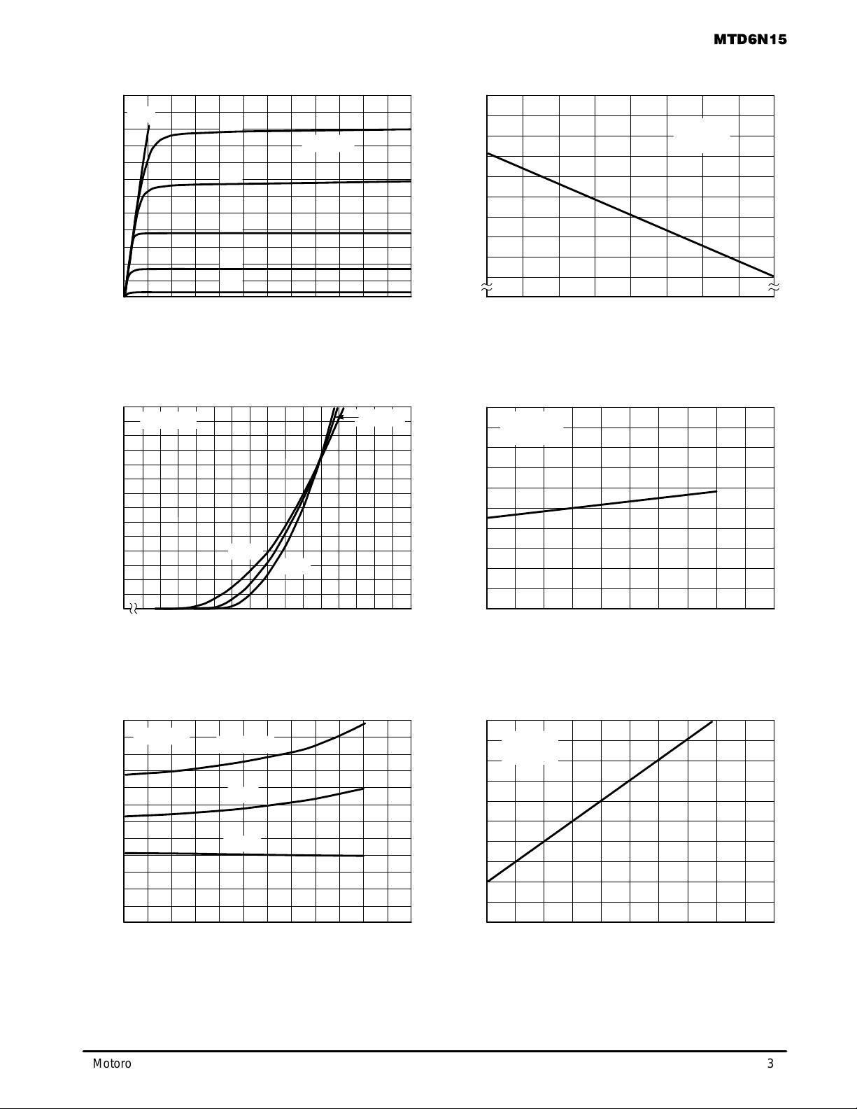
TYPICAL ELECTRICAL CHARACTERISTICS
2
1.6
1.2
0.8
0.4
0
VDS, DRAIN–TO–SOURCE VOLTAGE (VOLTS)
Figure 2. On–Region Characteristics
I
D
, DRAIN CURRENT (AMPS)
TJ = 25°C
24
20
16
12
8
4
0
6050403020100
10 V
9 V
8 V
7 V
6 V
5 V
VDS = V
GS
ID = 1 mA
–50 0 50 100 150
TJ, JUNCTION TEMPERATURE (
°
C)
Figure 3. Gate–Threshold Voltage Variation
With Temperature
V
GS(th)
, GATE THRESHOLD VOLTAGE (VOLTS)
3.6
3.2
2.8
2.4
2
I
D
, DRAIN CURRENT (AMPS)
VGS, GATE–TO–SOURCE VOLTAGE (VOLTS)
Figure 4. Transfer Characteristics
VDS = 10 V
TJ = 25°C
–55°C
100°C
14
12
10
8
6
4
2
0
4 6 8 10
2
1.6
1.2
0.8
0.4
0
–50 0 50 100 150 200
TJ, JUNCTION TEMPERATURE (
°
C)
Figure 5. Breakdown Voltage Variation
With Temperature
V
(BR)DSS
, DRAIN–TO–SOURCE BREAKDOWN VOLTAGE
(NORMALIZED)
VGS = 0 V
ID = 0.25 mA
R
DS(on)
, DRAIN–TO–SOURCE RESISTANCE (OHMS)
ID, DRAIN CURRENT (AMPS)
Figure 6. On–Resistance versus Drain Current
VGS = 10 V
0.30
0.25
0.20
0.15
0.10
0.05
0
201612840
TJ = 100°C
25°C
–55°C
R
DS(on)
, DRAIN–TO–SOURCE RESISTANCE
(NORMALIZED)
TJ, JUNCTION TEMPERATURE (°C)
Figure 7. On–Resistance Variation
With Temperature
VGS = 10 V
ID = 3 A
–50 0 50 100 150 200
Page 4

MTD6N15
4
Motorola TMOS Power MOSFET Transistor Device Data
SAFE OPERATING AREA
VDS, DRAIN–TO–SOURCE VOLTAGE (VOLTS)
Figure 8. Maximum Rated Forward Biased
Safe Operating Area
VDS, DRAIN–TO–SOURCE VOLTAGE (VOLTS)
Figure 9. Maximum Rated Switching
Safe Operating Area
I
D
, DRAIN CURRENT (AMPS)
R
DS(on)
LIMIT
THERMAL LIMIT
PACKAGE LIMIT
I
D
, DRAIN CURRENT (AMPS)
TJ ≤ 150°C
20
10
5
2
1
0.5
0.2
0.1
0.05
0.03
3002001007050302010753210.3 0.5 0.7
10 µs
1 ms
10 ms
dc
100 µs
TC = 25°C
VGS = 20 V SINGLE PULSE
20
15
10
5
0
0 20 40 60 80 100 120 140 160
FORWARD BIASED SAFE OPERATING AREA
The FBSOA curves define the maximum drain–to–source
voltage and drain current that a device can safely handle
when it is forward biased, or when it is on, or being turned on.
Because these curves include the limitations of simultaneous
high voltage and high current, up to the rating of the device,
they are especially useful to designers of linear systems. The
curves are based on a case temperature of 25°C and a maximum junction temperature of 150°C. Limitations for repetitive
pulses at various case temperatures can be determined by
using the thermal response curves. M otorola Application
Note, AN569, “Transient Thermal Resistance–General Data
and Its Use” provides detailed instructions.
SWITCHING SAFE OPERATING AREA
The switching safe operating area (SOA) of Figure 9 is the
boundary that the load line may traverse without incurring
damage to the M OSFET. The fundamental limits are t he
peak current, IDM and the breakdown voltage, V
(BR)DSS
. The
switching SOA shown in Figure 8 is applicable for both turn–
on and turn–off of the devices for switching times less than
one microsecond.
The power averaged over a complete switching cycle must
be less than:
T
J(max)
– T
C
R
θJC
t, TIME OR PULSE WIDTH (ms)
Figure 10. Thermal Response
r(t), EFFECTIVE TRANSIENT
THERMAL RESISTANCE (NORMALIZED)
R
θ
JC
(t) = r(t) R
θ
JC
R
θ
JC
(t) = 6.25
°
C/W MAX
D CURVES APPLY FOR POWER
PULSE TRAIN SHOWN
READ TIME AT t
1
T
J(pk)
– TC = P
(pk)
R
θ
JC
(t)
P
(pk)
t
1
t
2
DUTY CYCLE, D = t1/t
2
10000.01 0.02 0.03 0.05 0.1 0.2 0.3 0.5 1 2 3 5 10 20 50 100 200 500
0.01
0.02
0.03
0.05
0.07
0.1
0.2
0.3
0.5
0.7
D = 0.5
0.2
0.1
0.05
0.02
0.01
SINGLE PULSE
Page 5

MTD6N15
5
Motorola TMOS Power MOSFET Transistor Device Data
C
rss
GATE–TO–SOURCE OR DRAIN–TO–SOURCE VOLTAGE (VOLTS)
Figure 11. Capacitance Variation
C, CAPACITANCE (pF)
V
GS
V
DS
VDS = 0
0
2000
1600
1200
252010
0
510
Figure 12. Gate Charge versus
Gate–To–Source Voltage
Qg, TOTAL GATE CHARGE (nC)
16
0
0 8
12
8
4
12 16 20
5
15
400
VDS = 50 V
V
GS
, GATE SOURCE VOLTAGE (VOLTS)
TJ = 25°C
ID = 6 A
75 V
120 V
TJ = 25°C
VGS = 0
4
800
15 30 35
C
iss
C
oss
RESISTIVE SWITCHING
PULSE GENERATOR
V
DD
V
out
V
in
R
gen
50
Ω
z = 50
Ω
50
Ω
DUT
R
L
Figure 13. Switching Test Circuit
t
off
OUTPUT, V
out
INVERTED
t
on
t
r
t
d(off)
t
f
t
d(on)
90%90%
10%
INPUT, V
in
10%
50%
90%
50%
PULSE WIDTH
Figure 14. Switching Waveforms
Page 6

MTD6N15
6
Motorola TMOS Power MOSFET Transistor Device Data
INFORMATION FOR USING THE DPAK SURFACE MOUNT PACKAGE
RECOMMENDED FOOTPRINT FOR SURFACE MOUNTED APPLICATIONS
Surface mount board layout is a critical portion of the total
design. The footprint for the semiconductor packages must be
the correct size to ensure proper solder connection interface
between the board and the package. With the correct pad
geometry, the packages will self align when subjected to a
solder reflow process.
0.190
4.826
mm
inches
0.100
2.54
0.063
1.6
0.165
4.191
0.118
3.0
0.243
6.172
POWER DISSIPATION FOR A SURFACE MOUNT DEVICE
The power dissipation for a surface mount device is a
function of the drain pad size. These can vary from the
minimum pad size for soldering to a pad size given for
maximum power dissipation. Power dissipation for a surface
mount device is determined by T
J(max)
, the maximum rated
junction temperature of the die, R
θJA
, the thermal resistance
from the device junction to ambient, and the operating
temperature, TA. Using the values provided on the data sheet,
PD can be calculated as follows:
PD =
T
J(max)
– T
A
R
θJA
The values for the equation are found in the maximum
ratings table on the data sheet. Substituting these values into
the equation for an ambient temperature TA of 25°C, one can
calculate the power dissipation of the device. For a DPAK
device, PD is calculated as follows.
= 1.75 Watts
The 71.4°C/W for the DPAK package assumes the use of
the recommended footprint on a glass epoxy printed circuit
board to achieve a power dissipation of 1.75 Watts. There are
other alternatives to achieving higher power dissipation from
the surface mount packages. One is to increase the area of the
drain pad. By increasing the area of the drain pad, the power
dissipation can be increased. Although one can almost double
the power dissipation with this method, one will be giving up
area on the printed circuit board which can defeat the purpose
of using surface mount technology. For example, a graph of
R
θJA
versus drain pad area is shown in Figure 15.
1.75 Watts
Board Material = 0.0625
″
G–10/FR–4, 2 oz Copper
80
100
60
40
20
1086420
3.0 Watts
5.0 Watts
TA = 25°C
A, AREA (SQUARE INCHES)
TO AMBIENT ( C/W)
°
R
JA
, THERMAL RESISTANCE, JUNCTION
θ
Another alternative would be to use a ceramic substrate or
an aluminum core board such as Thermal Clad. Using a
board material such as Thermal Clad, an aluminum core
board, the power dissipation can be doubled using the same
footprint.
150°C – 25°C
PD =
71.4°C/W
Figure 15. Thermal Resistance versus Drain Pad
Area for the DPAK Package (Typical)
Page 7

MTD6N15
7
Motorola TMOS Power MOSFET Transistor Device Data
SOLDER STENCIL GUIDELINES
Prior to placing surface mount components onto a printed
circuit board, solder paste must be applied to the pads. Solder
stencils are used to screen the optimum amount. These
stencils are typically 0.008 inches thick and may be made of
brass or stainless steel. For packages such as the SC–59,
SC–70/SOT–323, SOD–123, SOT–23, SOT–143, SOT–223,
SO–8, SO–14, SO–16, and SMB/SMC diode packages, the
stencil opening should be the same as the pad size or a 1:1
registration. This is not the case with the DPAK and D2PAK
packages. If one uses a 1:1 opening to screen solder onto the
drain pad, misalignment and/or “tombstoning” may occur due
to an excess of solder. For these two packages, the opening
in the stencil for the paste should be approximately 50% of the
tab area. The opening for the leads is still a 1:1 registration.
Figure 16 shows a typical stencil for the DPAK and D2PAK
packages. The pattern of the opening in the stencil for the
drain pad is not critical as long as it allows approximately 50%
of the pad to be covered with paste.
Figure 16. Typical Stencil for DPAK and
D2PAK Packages
SOLDER PASTE
OPENINGS
STENCIL
SOLDERING PRECAUTIONS
The melting temperature of solder is higher than the rated
temperature of the device. When the entire device is heated
to a high temperature, failure to complete soldering within a
short time could result in device failure. Therefore, the
following items should always be observed in order to
minimize the thermal stress to which the devices are
subjected.
• Always preheat the device.
• The delta temperature between the preheat and soldering
should be 100°C or less.*
• When preheating and soldering, the temperature of the
leads and the case must not exceed the maximum
temperature ratings as shown on the data sheet. When
using infrared heating with the reflow soldering method,
the difference shall be a maximum of 10°C.
• The soldering temperature and time shall not exceed
260°C for more than 10 seconds.
• When shifting from preheating to soldering, the maximum
temperature gradient shall be 5°C or less.
• After soldering has been completed, the device should be
allowed to cool naturally for at least three minutes.
Gradual cooling should be used as the use of forced
cooling will increase the temperature gradient and result
in latent failure due to mechanical stress.
• Mechanical stress or shock should not be applied during
cooling.
* Soldering a device without preheating can cause excessive
thermal shock and stress which can result in damage to the
device.
* Due to shadowing and the inability to set the wave height to
incorporate other surface mount components, the D2PAK is
not recommended for wave soldering.
Page 8

MTD6N15
8
Motorola TMOS Power MOSFET Transistor Device Data
TYPICAL SOLDER HEATING PROFILE
For any given circuit board, there will be a group of control
settings that will give the desired heat pattern. The operator
must set temperatures for several heating zones, and a figure
for belt speed. T aken together , these control settings make up
a heating “profile” for that particular circuit board. On
machines controlled by a computer, the computer remembers
these profiles from one operating session to the next. Figure
17 shows a typical heating profile for use when soldering a
surface mount device to a printed circuit board. This profile will
vary among soldering systems but it is a good starting point.
Factors that can affect the profile include the type of soldering
system in use, density and types of components on the board,
type of solder used, and the type of board or substrate material
being used. This profile shows temperature versus time. The
line on the graph shows the actual temperature that might be
experienced on the surface of a test board at or near a central
solder joint. The two profiles are based on a high density and
a low density board. The Vitronics SMD310 convection/infrared reflow soldering system was used to generate this
profile. The type of solder used was 62/36/2 Tin Lead Silver
with a melting point between 177–189°C. When this type of
furnace is used for solder reflow work, the circuit boards and
solder joints tend to heat first. The components on the board
are then heated by conduction. The circuit board, because it
has a large surface area, absorbs the thermal energy more
efficiently, then distributes this energy to the components.
Because of this effect, the main body of a component may be
up to 30 degrees cooler than the adjacent solder joints.
STEP 1
PREHEAT
ZONE 1
“RAMP”
STEP 2
VENT
“SOAK”
STEP 3
HEATING
ZONES 2 & 5
“RAMP”
STEP 4
HEATING
ZONES 3 & 6
“SOAK”
STEP 5
HEATING
ZONES 4 & 7
“SPIKE”
STEP 6
VENT
STEP 7
COOLING
200
°
C
150
°
C
100
°
C
50
°
C
TIME (3 TO 7 MINUTES TOTAL)
T
MAX
SOLDER IS LIQUID FOR
40 TO 80 SECONDS
(DEPENDING ON
MASS OF ASSEMBLY)
205
°
TO 219°C
PEAK AT
SOLDER JOINT
DESIRED CURVE FOR LOW
MASS ASSEMBLIES
100°C
150°C
160
°
C
170°C
140
°
C
Figure 17. Typical Solder Heating Profile
DESIRED CURVE FOR HIGH
MASS ASSEMBLIES
Page 9

MTD6N15
9
Motorola TMOS Power MOSFET Transistor Device Data
PACKAGE DIMENSIONS
CASE 369A–13
ISSUE W
STYLE 2:
PIN 1. GATE
2. DRAIN
3. SOURCE
4. DRAIN
D
A
K
B
R
V
S
F
L
G
2 PL
M
0.13 (0.005) T
E
C
U
J
H
–T–
SEATING
PLANE
Z
DIM MIN MAX MIN MAX
MILLIMETERSINCHES
A 0.235 0.250 5.97 6.35
B 0.250 0.265 6.35 6.73
C 0.086 0.094 2.19 2.38
D 0.027 0.035 0.69 0.88
E 0.033 0.040 0.84 1.01
F 0.037 0.047 0.94 1.19
G 0.180 BSC 4.58 BSC
H 0.034 0.040 0.87 1.01
J 0.018 0.023 0.46 0.58
K 0.102 0.114 2.60 2.89
L 0.090 BSC 2.29 BSC
R 0.175 0.215 4.45 5.46
S 0.020 0.050 0.51 1.27
U 0.020 ––– 0.51 –––
V 0.030 0.050 0.77 1.27
Z 0.138 ––– 3.51 –––
NOTES:
1. DIMENSIONING AND TOLERANCING PER ANSI
Y14.5M, 1982.
2. CONTROLLING DIMENSION: INCH.
Page 10

MTD6N15
10
Motorola TMOS Power MOSFET Transistor Device Data
How to reach us:
USA /EUROPE: Motorola Literature Distribution; JAPAN: Nippon Motorola Ltd.; Tatsumi–SPD–JLDC, Toshikatsu Otsuki,
P.O. Box 20912; Phoenix, Arizona 85036. 1–800–441–2447 6F Seibu–Butsuryu–Center, 3–14–2 Tatsumi Koto–Ku, Tokyo 135, Japan. 03–3521–8315
MFAX: RMFAX0@email.sps.mot.com – TOUCHTONE (602) 244–6609 HONG KONG: Motorola Semiconductors H.K. Ltd.; 8B Tai Ping Industrial Park,
INTERNET: http://Design–NET.com 51 Ting Kok Road, Tai Po, N.T., Hong Kong. 852–26629298
Motorola reserves the right to make changes without further notice to any products herein. Motorola makes no warranty , representation or guarantee regarding
the suitability of its products for any particular purpose, nor does Motorola assume any liability arising out of the application or use of any product or circuit,
and specifically disclaims any and all liability, including without limitation consequential or incidental damages. “T ypical” parameters can and do vary in different
applications. All operating parameters, including “T ypicals” must be validated for each customer application by customer’s technical experts. Motorola does
not convey any license under its patent rights nor the rights of others. Motorola products are not designed, intended, or authorized for use as components in
systems intended for surgical implant into the body, or other applications intended to support or sustain life, or for any other application in which the failure of
the Motorola product could create a situation where personal injury or death may occur. Should Buyer purchase or use Motorola products for any such
unintended or unauthorized application, Buyer shall indemnify and hold Motorola and its officers, employees, subsidiaries, affiliates, and distributors harmless
against all claims, costs, damages, and expenses, and reasonable attorney fees arising out of, directly or indirectly, any claim of personal injury or death
associated with such unintended or unauthorized use, even if such claim alleges that Motorola was negligent regarding the design or manufacture of the part.
Motorola and are registered trademarks of Motorola, Inc. Motorola, Inc. is an Equal Opportunity/Affirmative Action Employer.
MTD6N15/D
*MTD6N15/D*
◊
 Loading...