

Page 1
without notice. No liability is assumed as a result of the use of this procuts. No rights under any patent accompany the sales o
MYSON
GENERAL DESCRIPTION
IEEE802.3 and IEEE802.3u compliant.
packet filtering function.
4MB/2MB packet buffer with SGRAM/SDRAM
flexible memory interface.
Build in internal/external memory test function.
The MTD516 complies fully with the
The MTD516 provides EEPROM interface
agement interface.
MTD516
TECHNOLOGY
16 Port 10M/100M Ethernet Switch
FEATURES
•
• Provide 16 RMII (Reduced Media Independent
Interface) ports.
• Programmable 1K/8K MAC addresses filtering
database.
• Store and forward switching function and bad
• Optional back_pressure/802.3x flow control/
flooding control/broadcast control.
• Optional EEPROM Interface for advanced
switch configurations.
•
• Port VLAN/trunking.
• Link/Rx activity, packet buffer utilization LED
display.
• 83MHz for non-blocking 16 port switch.
•
• 208 pin PQFP package, 3.3V operation voltage.
(Preliminary)
IEEE802.3, 802.3u and 802.3x specifications and
is a non-blocking 16 port 10M/100M Ethernet
switch device.
Support 16 RMII ports for 10M/100M operation. 4MB memory interface provides maximum
2730 packet buffers for Ethernet packet buffering.
Up to 8192 address entrys are provided by the
MTD516, and the MTD516 use full Ethernet
address compare algorithm to minimize hashing
collision events.
to config port trunking, port VLAN, static entry,
802.3x flow control threshold, flooding port,
broadcast control threshold. Each MTD516 ports
support 10M/100M auto-negotiation by MII man-
The MTD516 also provides 2 pins for Link/
RX activity, packet buffer utilization LED display
function.
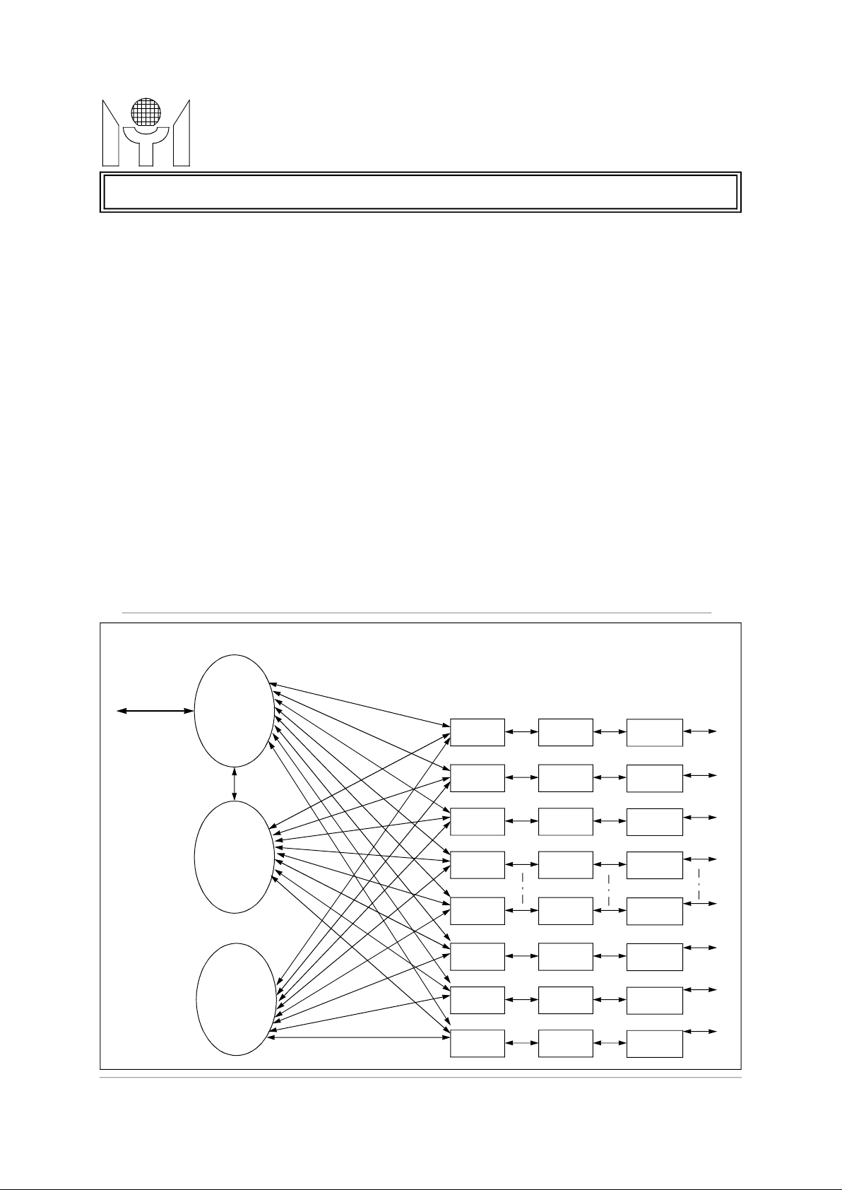
BL OCK DIAGRAM
SDRAM/
SGRAM
Interface
Memory
Controller
Memor y
Arbiter
Port
Switch
Logic
MAC0DMA0
MAC1DMA1
MAC2DMA2
MAC3DMA3
MAC4DMA4
MAC13DMA13
MAC14DMA14
MAC15DMA15
RMII0
RMII1
RMII2
RMII3
3~12
RMII12
RMII13
RMII14
RMII15
This datasheet contains new product information. Myson Technology reserves the rights to modify the product specification
the product.
1/27 MTD516 Revision 1.2 19/06/2000
f
Page 2
without notice. No liability is assumed as a result of the use of this procuts. No rights under any patent accompany the sales o
MYSON
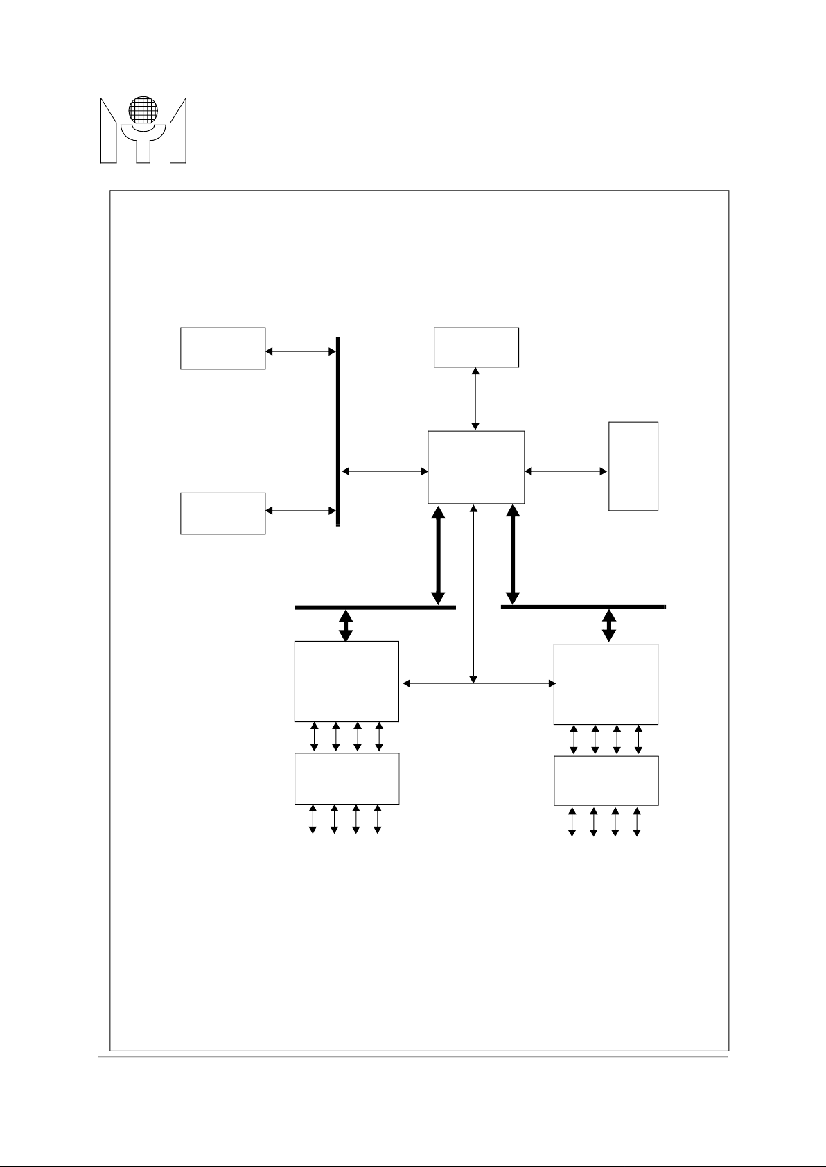
SYSTEM DIA GRAM
RMII11-15
Transfor mer
(**Pr ogra m mab le)
MII mana gement
MTD516
TECHNOLOGY
SGRAM
(512kx32x2)
SGRAM
(256kx32x2)
(**OPT I O N)
EEPROM
MTD516
(Preliminary)
LEDs
RMII 0-7
OCTAL
PHYsceiv er
OCTAL
Transfor mer
RJ45 RJ45
OCTAL
PHYsceiver
OCTAL
This datasheet contains new product information. Myson Technology reserves the rights to modify the product specification
the product.
2/27 MTD516 Revision 1.2 19/06/2000
f
Page 3

MTD516 Revision 1.2 19/06/2000
MYSON
MTD516
TECHNOLOGY
1.0 PIN CONNECTION
DQ9
DQ8
DQ0
DQ1
DQ2
DQ3
DQ4
DQ5
DQ6
156
155
154
153
152
151
150
149
DQ10
DQ11
GND
VCC
DQ12
DQ13
DQ14
DQ15
DQ24
DQ25
DQ26
DQ27
DQ28
DQ29
DQ30
DQ31
LEDDATA
LEDCLK
EEDATA
EECLK
GND
REFCLK
VCC
RESETB
MDC
MDIO
TXD0_1
TXD0_0
TXEN0
CRSDV0
RXD0_0
RXD0_1
GND
VCC
TXD1_1
TXD1_0
TXEN1
CRSDV1
RXD1_0
RXD1_1
TXD2_1
TXD2_0
TXEN2
CRSDV2
RXD2_0
RXD2_1
TXD3_1
TXD3_0
TXEN3
CRSDV3
RXD3_0
RXD3_1
157
158
159
160
161
162
163
164
165
166
167
168
169
170
171
172
173
174
175
176
177
178
179
180
181
182
183
184
185
186
187
188
189
190
191
192
193
194
195
196
197
198
199
200
201
202
203
204
205
206
207
208
148
(Preliminary)
DQ7
DQ16
DQ17
DQ18
DQ19
DQ20
VCC
GND
DQ21
DQ22
DQ23
WEB
CASB
RASB
CS0BBAAD0
AD1
AD2
AD3
AD4
AD5
AD6
AD7
AD8
VCC
MEMCLK
GND
DQ63
DQ62
DQ61
DQ60
DQ59
DQ58
DQ57
DQ56
DQ47
DQ46
DQ45
DQ44
VCC
GND
DQ43
147
146
145
144
143
142
141
140
139
138
137
136
135
134
133
132
131
130
129
128
127
126
125
124
123
122
121
120
119
118
117
116
115
114
113
112
111
110
109
108
107
106
105
104
DQ42
103
DQ41
102
DQ40
101
DQ32
100
DQ33
99
DQ34
98
DQ35
97
DQ36
96
DQ37
95
VCC
94
GND
93
DQ38
92
DQ39
91
DQ48
90
DQ49
89
DQ50
88
DQ51
87
DQ52
86
DQ53
85
DQ54
84
DQ55
83
VCC
82
MTD516
81
80
79
78
77
76
75
74
73
72
71
70
69
68
67
66
65
64
63
62
61
60
59
58
57
56
55
54
53
SYSCLK
GND
RXD15_1
RXD15_0
CRSDV15
TXEN15
TXD15_0
TXD15_1
RXD14_1
RXD14_0
CRSDV14
TXEN14
TXD14_0
TXD14_1
VCC
GND
RXD13_1
RXD13_0
CRSDV13
TXEN13
TXD13_0
TXD13_1
RXD12_1
RXD12_0
CRSDV12
TXEN12
TXD12_0
TXD12_1
RXD11_1
RXD11_0
010203040506070809101112131415161718192021222324252627282930313233343536373839404142434445464748495051
TXD4_1
TXD4_0
TXEN4
CRSDV4
RXD4_0
RXD4_1
TXD5_1
TXD5_0
TXEN5
GND
VCC
CRSDV5
RXD5_0
RXD5_1
TXD6_1
TXD6_0
TXEN6
CRSDV6
RXD6_0
RXD6_1
TXD7_1
TXD7_0
TXEN7
CRSDV7
RXD7_0
RXD7_1
GND
VCC
TXD8_1
TXD8_0
TXEN8
CRSDV8
RXD8_0
RXD8_1
TXD9_1
TXD9_0
TXEN9
CRSDV9
RXD9_0
RXD9_1
GND
VCC
TXD10_1
TXD10_0
TXEN10
CRSDV10
RXD10_0
RXD10_1
TXD11_1
TXD11_0
3/27
52
TXEN11
CRSDV11
Page 4

MTD516 Revision 1.2 19/06/2000
MYSON
RMII Port Inter f ace Pins
Port0 RMII receive interface signal, CRSDV0 is asserted high when
port0 media is non_idle.
Port0 RMII transmit enable signal.
Port0 RMII transmit data bit_0.
Port0 RMII transmit data bit_1.
Port1 RMII receive interface signal, CRSDV1 is asserted high when
port1 media is non_idle.
Port1 RMII transmit enable signal.
Port1 RMII transmit data bit_0.
Port1 RMII transmit data bit_1.
Port2 RMII receive interface signal, CRSDV2 is asserted high when
port2 media is non_idle.
Port2 RMII transmit enable signal.
Port2 RMII transmit data bit_0.
Port2 RMII transmit data bit_1.
Port3 RMII receive interface signal, CRSDV0 is asserted high when
port3 media is non_idle.
Port3 RMII transmit enable signal.
Port3 RMII transmit data bit_0.
Port3 RMII transmit data bit_1.
Port4 RMII/MII receive interface signal, CRSDV4 is asserted high when
port4 media is non_idle.
Port4 RMII transmit enable signal
Port5 RMII receive interface signal, CRSDV5 is asserted high when
port5 media is non_idle.
Port5 RMII transmit enable signal.
Port5 RMII transmit data bit_0.
Port5 RMII transmit data bit_1.
MTD516
TECHNOLOGY
2.0 PIN DESCRIPTIONS
Name Pin Number I/O Descriptio ns
CRSDV0
RXD0_0
RXD0_1
TXEN0
TXD0_0
TXD0_1
CRSDV1
RXD1_0
RXD1_1
TXEN1
TXD1_0
TXD1_1
CRSDV2
186
187
188
185
184
183
194
195
196
193
192
191
200
I
IIPort0 RMII receive data bit_0.
Port0 RMII receive data bit_1.
O
O
O
I
IIPort1 RMII receive data bit_0.
Port1 RMII receive data bit_1.
O
O
O
I
(Preliminary)
RXD2_0
RXD2_1
TXEN2
TXD2_0
TXD2_1
CRSDV3
RXD3_0
RXD3_1
TXEN3
TXD3_0
TXD3_1
CRSDV4
RXD4_0
RXD4_1
TXEN4
TXD4_0
TXD4_1
CRSDV5
201
202
199
198
197
206
207
208
205
204
203
4
5
6
3
2
1
12
IIPort2 RMII receive data bit_0.
Port2 RMII receive data bit_1.
O
O
O
I
IIPort3 RMII receive data bit_0.
Port3 RMII receive data bit_1.
O
O
O
I
IIPort4 RMII/MII receive data bit_0.
Port4 RMII/MII receive data bit_1.
O
OOPort4 RMII/MII transmit data bit_0.
Port4 RMII/MII transmit data bit_1.
I
RXD5_0
RXD5_1
TXEN5
TXD5_0
TXD5_1
13
14
9
8
7
IIPort5 RMII receive data bit_0.
Port5 RMII receive data bit_1.
O
O
O
4/27
Page 5

MTD516 Revision 1.2 19/06/2000
MYSON
Port6 RMII receive interface signal, CRSDV6 is asserted high when
port6 media is non_idle.
Port6 RMII transmit enable signal.
Port6 RMII transmit data bit_0.
Port6 RMII transmit data bit_1.
Port7 RMII receive interface signal, CRSDV7 is asserted high when
port7 media is non_idle.
Port7 RMII transmit enable signal.
Port7 RMII transmit data bit_0.
Port7 RMII transmit data bit_1.
Port8 RMII receive interface signal, CRSDV8 is asserted high when
port8 media is non_idle.
Port8 RMII transmit enable signal.
Port8 RMII transmit data bit_0.
Port8 RMII transmit data bit_1.
Port9 RMII receive interface signal, CRSDV9 is asserted high when
port9 media is non_idle.
Port9 RMII transmit enable signal.
Port9 RMII transmit data bit_0.
Port9 RMII transmit data bit_1.
Port10 RMII receive interface signal, CRSDV10 is asserted high when
port10 media is non_idle.
Port11 RMII receive interface signal, CRSDV11 is asserted high when
port11 media is non_idle.
Port11 RMII receive data bit_0.
Port11 RMII receive data bit_1.
Port11 RMII transmit enable signal.
Port11 RMII transmit data bit_0.
Port11 RMII transmit data bit_1.
RMII Port Inter f ace Pins
MTD516
TECHNOLOGY
Name Pin Number I/O Descriptio ns
CRSDV6
RXD6_0
RXD6_1
TXEN6
TXD6_0
TXD6_1
CRSDV7
RXD7_0
RXD7_1
TXEN7
TXD7_0
TXD7_1
CRSDV8
18
19
20
17
16
15
24
25
26
23
22
21
32
I
IIPort6 RMII receive data bit_0.
Port6 RMII receive data bit_1.
O
O
O
I
IIPort7 RMII receive data bit_0.
Port7 RMII receive data bit_1.
O
O
O
I
(Preliminary)
RXD8_0
RXD8_1
TXEN8
TXD8_0
TXD8_1
CRSDV9
RXD9_0
RXD9_1
TXEN9
TXD9_0
TXD9_1
CRSDV10
RXD10_0
RXD10_1
TXEN10
TXD10_0
TXD10_1
CRSDV11
33
34
31
30
29
38
39
40
37
36
35
46
47
48
45
44
43
52
IIPort8 RMII receive data bit_0.
Port8 RMII receive data bit_1.
O
O
O
I
IIPort9 RMII receive data bit_0.
Port9 RMII receive data bit_1.
O
O
O
I
IIPort10 RMII receive data bit_0.
Port10 RMII receive data bit_1.
O Port10 RMII transmit enable signal.
OOPort10 RMII transmit data bit_0.
Port10 RMII transmit data bit_1.
I
RXD11_0
RXD11_1
TXEN11
TXD11_0
TXD11_1
53
54
51
50
49
I
I
O
O
O
5/27
Page 6

MTD516 Revision 1.2 19/06/2000
MYSON
Port12 RMII receive interface signal, CRSDV12 is asserted high when
port12 media is non_idle.
Port12 RMII transmit enable signal.
Port12 RMII transmit data bit_0.
Port12 RMII transmit data bit_1.
Port13 RMII receive interface signal, CRSDV13 is asserted high when
port13 media is non_idle.
Port13 RMII transmit enable signal.
Port13 RMII transmit data bit_0.
Port13 RMII transmit data bit_1.
Port14 RMII receive interface signal, CRSDV14 is asserted high when
port14 media is non_idle.
Port14 RMII transmit enable signal.
Port14 RMII transmit data bit_0.
Port14 RMII transmit data bit_1.
Port15 RMII receive interface signal, CRSDV15 is asserted high when
port15 media is non_idle.
Port15 RMII transmit enable signal.
Port15 RMII transmit data bit_0.
Port15 RMII transmit data bit_1.
RMII Port Inter f ace Pins
MTD516
TECHNOLOGY
Name Pin Number I/O Descripti ons
CRSDV12
RXD12_0
RXD12_1
TXEN12
TXD12_0
TXD12_1
CRSDV13
RXD13_0
RXD13_1
TXEN13
TXD13_0
TXD13_1
CRSDV14
58
59
60
57
56
55
64
65
66
63
62
61
72
I
IIPort12 RMII receive data bit_0.
Port12 RMII receive data bit_1.
O
O
O
I
IIPort13 RMII receive data bit_0.
Port13 RMII receive data bit_1.
O
O
O
I
(Preliminary)
RXD14_0
RXD14_1
TXEN14
TXD14_0
TXD14_1
CRSDV15
RXD15_0
RXD15_1
TXEN15
TXD15_0
TXD15_1
73
74
71
70
69
78
79
80
77
76
75
IIPort14 RMII receive data bit_0.
Port14 RMII receive data bit_1.
O
O
O
I
IIPort15 RMII receive data bit_0.
Port15 RMII receive data bit_1.
O
O
O
6/27
Page 7
MTD516 Revision 1.2 19/06/2000
MYSON
Note: SGRAM/SDRAM access time: 10 ns (max)
Synch ro n o u s DRAM/GRAM Interface Pins
Memory row/column address bus outputs
AD[7:0] are row/column address [7:0].
Memory data bus DQ[63:56] : 119~112
DQ[47:44] : 111~108
DQ[11:8] : 158~155
SGRAM/SDRAM row address select
SGRAM/SDRAM write enable
Memory chip select 0
Memory clock output.
Miscellaneous Pins
System reset input, low active.
Switch core system clock input
MII management clock inout.
MII management data inout
After 150 ms, it indicate SDC.
After 150 ms, it indicate SDIO.
MTD516
TECHNOLOGY
Name Pin Number I/O Descriptions
AD[8:0]
123~131
DQ[63:0]
RASB 134 O
CASB 135 O SGRAM/SDRAM column address select
WEB 136 O
BA 132 O SGRAM/SDRAM bank select
CS0B 133 O
MEMCLK 121 O
119~112,
84~91,
111~108,
105~102,
92~93,
96~101,
172~165,
137~139,
142~146,
164~161,
158~155,
147~154
O
AD[8] : This pin should connect to SGRAM/SDRAM MSB address bit.
I/O
DQ[55:48] : 84~91
DQ[43:40] : 105~102
DQ[39:38] : 92~93
DQ[37:32] : 96~101
DQ[31:24] : 172~165
DQ[23:21] : 137~139
DQ[20:16] : 142~146
DQ[15:12] : 164~161
DQ[7:0] : 147~154
(Preliminary)
Name Pin Number I/O Descriptions
RESETB 180 I
SYSCLK 82 I
REFCLK 178 I RMII reference clock input
MDC 181 I/O
MDIO 182 I/O
EECLK/
SDC
EEDATA/
SDIO
LEDCLK
176
175
174
I/O After ResetB deassert to ? ms , this pin indicate EECLK,
I/O After ResetB deassert to ? ms , this pin be indicated EEDATA,
I/O LED Clock.
Using bursted clock for latching 32 display informations (one clock
latch one information) , per burst have 32 continuous clocks (clock
period = 320 ns); and the time between burst to burst is 655 us.
7/27
Page 8

MTD516 Revision 1.2 19/06/2000
MYSON
The serial output display informations using bursted styling ,per burst
have 32 informations, as following:
01 P0_RxAct 17 Uti_1%
02 P1_RxAct 18 Uti_3%
03 P2_RxAct 19 Uti_5%
04 P3_RxAct 20 Uti_10%
05 P4_RxAct 21 Uti_15%
06 P5_RxAct 22 Uti_20%
07 P6_RxAct 23 Uti_30%
08 P7_RxAct 24 Uti_35%
09 P8_RxAct 25 Uti_40%
10 P9_RxAct 26 Uti_50%
11 P10_RxAct 27 Uti_60%
12 P11_RxAct 28 Uti_70%
16 P15_RxAct 32 MemTestFail
Miscellaneous Pins
MTD516
TECHNOLOGY
Name Pin Number I/O Descriptions
LEDDA TA
173
I/O LED Data (high_active).
LEDCLK LEDDATA LEDCLK LEDDATA
(Preliminary)
VCC 1 1,28,42,68,
83,95,107,
122,141,160,
179,190,
GND 10,27,41,67,
81,94,106,
120,140,159,
177,189,
13 P12_RxAct 29 Uti_80%
14 P13_RxAct 30 Uti_90%
15 P14_RxAct 31 BufferAlarm
PWR Power pins
GND Ground pins
8/27
Page 9

MTD516 Revision 1.2 19/06/2000
MYSON
Power on Setti ng Config uratio n
Jump er Configu ratio n After Power On Reset
802.3x flow control function enable.
external pull_hgih =1, 802.3x flow control enable.
external pull_low = 0, backpressure disable.
external pull_hgih =1, memory BIST enable.
external pull_low = 0, memory BIST disable.
external pull_hgih =1, chip fast test mode enable.
external pull_hgih =1, chip scan test mode enable.
8K entry address table enable.
external pull_low = 0, 8K address table disable; defaule is 1K entry.
Auto_load from EEPROM function enable.
Broadcast storm protect function enable.
external pull_hgih =1, 12 port switch enable.
Port 15 FX function indicator.
MTD516
TECHNOLOGY
3.0
Pin Name Function
MDC
FlowCtrlEn
EECLK
BakPsureEn
EEDA TA
MiiPollEn
LEDCLK
AgingEn
LEDDA TA
BISTEn
(Preliminary)
defa
ult
1
external pull_low = 0, 802.3x flow control disable.
1 In Half duplex mode, backpressure function enable.
external pull_hgih =1, backpressure enable.
1 Polling PHY device’s MII register function enable.
external pull_hgih =1, PHY auto polling enable.
external pull_low = 0, PHY auto polling disable.
1 Aging out function for address learning enable.
external pull_hgih =1, aging out function enable.
external pull_low = 0, aging out function disable.
1 Embbeded memory self-test function enable.
Descriptio ns
TXEN13
TXEN12
TXEN11
TXEN10
TXEN9
TXEN8
TXEN7
FastMode
ScanMode
8KAddrTblEn
EEPROMEn
BroadStor-
mEn
En12PortSW
P15FXEn
0 For chip test only.
external pull_low = 0, chip fast test mode disable.
0 For chip test only.
external pull_low = 0, chip scan test mode disable.
0
external pull_hgih =1, 8K address table enable.
0
external pull_hgih =1, auto load from EEPROM function enable.
external pull_low = 0, auto load from EEPROM function disable.
0
external pull_hgih =1, broadcast storm protection enable.
external pull_low = 0, broadcast storm protection disable.
0 For 12 port switch, only Port11~Port0 enable.
external pull_low = 0, default is 16 port switch.
0
external pull_hgih =1, port15 FX function enable.
external pull_low = 0, port15 FX function disable.
9/27
Page 10

MTD516 Revision 1.2 19/06/2000
MYSON
Port15 duplex ability indicator (under port15 configured in FX mode).
external pull_hgih =1, port15 operate in full_duplex mode.
external pull_low = 0, VLAN tag 1522 bytes acceptance enable disable.
external pull_low = 0.
external pull_low = 0.
external pull_low = 0.
external pull_low = 0.
Jump er Configu ratio n After Power On Reset
MTD516
TECHNOLOGY
Pin Name Function
TXEN6
P15Full
TXEN5
En1522
TXEN4
FloodCtrlEn
TXEN3
FloodID[3]
TXEN2
FloodID[2]
(Preliminary)
defa
ult
0
external pull_low = 0, port15 operate in half_duplex mode.
0 VLAN tag 1522 bytes acceptance function enable.
external pull_hgih =1, VLAN tag 1522 bytes acceptance enable.
0 Flooding control function enable.
external pull_hgih =1, flooding control function enable.
external pull_low = 0, flooding control function disable.
0 Flooding Port ID bit 3
external pull_hgih =1.
0 Flooding Port ID bit 2
external pull_hgih =1.
Descriptio ns
TXEN1
TXEN0
FloodID[1]
FloodID[0]
0 Flooding Port ID bit 1
external pull_hgih =1.
0 Flooding Port ID bit 0
external pull_hgih =1.
10/27
Page 11

MTD516 Revision 1.2 19/06/2000
MYSON
4.0 FUNCTIONAL DESCRIPTIONS
4.1 Packet sto re and for w ardi n g
each good unicast packet is completely received. The static address learning is achieved by EEPROM
tured. If the DA can not get a hit result, the packet is going to switch broadcast or forward to the dedi-
The buffer queue manager is implemented to manage the external shared memory (use SDRAM/
4.5 Ful l Dupl ex 802.3x Flow Cont r o l
queue’s on_using value reach the initialization setting threshold value(recommended XON_TH = 40’h
to the initialization threshold value(recommended Xoff_TH = 1C’h when using 2Mbytes external mem-
MTD516
TECHNOLOGY
The MTD516 is an 16 ports 10/100 Mbps fast Ethernet switch controller. It is a low cost solution for sixteen ports fast Ethernet SOHO switch design. No CPU interface is required; After power on reset,
MTD516 provide an auto load configuration setting function through a 2 wire serial EEPROM interface
to acess external EEPROM device, and MTD516 can easily be configured to support port_trunking,
port_ VLAN, static entry, 802.3X flow control threshold setting , flooding port assignment ...etc functions. The following descriptions are MTD516’s major functional blocks overview.
The MTD516 use simple store and forward algorithm as packet switching method. Input packet from
ports will be stored to external memory first, while packet is good for forward (CRC chech ok, 64Bytes <
length < 1518Bytes, not local packets, in the same VLAN group ) , if this packet’s DA hits, than forward
this packet to the destination port, otherwise this packet will be broadcasted.
4.2 Learning and Routi ng
The MTD516 supports 1K or 8K MAC entries for switching. Dynamic address learning is performed by
configuration. On the other hand, the routing process is performed whenever the packet’s DA is capcated port according to the flooding control selction.
(Preliminary)
4.3 Aging
Only the dynamic address entries are scheduled in the aging machine. If one station does not transmit
any packet for a period of time, the belonging MAC address will be kicked out from the address table.
The aging out time can be program through the EEPROM auto load configuration. (Default value is 300
seconds)
4.4 Buffer Queue Management
SGRAM) for packet buffering. The main function of the buffer queue manager is to maintain the linked
list consists of buffer IDs, which is used to show the corresponding memory address for each incoming
packet. In addition, the buffer queue manager monitors the rested free spaces status of the external
memory, If the packet storage achieve the predefined threshold value, the buffer queue manager will
raise the alarm signal which is used to enable the flow control mechanism for avoi ding transmission ID
queue overflow happening. MTD516 provide 802.3x flow control in full duplex mode and back pressure
control in half duplex mode.
In full duplex mode, MTD516 supports the standard flow control defined in IEEE802.3x standard. It
enables the stopping of remote node t ransmissions via a PAUSE frame information interactoin. When
the “802.3x flow control enable” bit is setted during power on reset (MDC pin is external pull_high),
it enables MTD516 supporting 802.3x flow control function in full_duplex mode; When output port buffer
under total free ID less then 100’h), MTD516 will send out a PAUSE packet with pause time equal to
FFF to stop the remote node transmission; When the output port buffer queue’s on_using value reduce
ory), MTD516 will also send a PAUSE packet with pause time equal to zero to inform the remote node
to retransmit packet.
4.6 Half Duplex Back Pressu r e Contro l
In half duplex mode, MTD516 provide a back pressure control mechanism to avoid dropping packets
during network conjection situation. When the “back pressure control enable” bit is set during power on
11/27
Page 12

MTD516 Revision 1.2 19/06/2000
MYSON
4.7 MII Polling
4.8 MAC and DMA engi ne
Tx_engine will constantly monitor the line traffic using derfering precedure. Only if it has been idle for a
pleted by address learning/routing process and buffer queue management operation.
4.9 EEPROM inter face
to acess external EEPROM device(24C02) after power on reset . MTD516 can easily be configured to
assignment ...etc functions.
The MTD516 supports VLAN configuration by port based methodology. One port select the certain
is not forwarding to the destination port whose VLAN group is different from the source port.
4.11 Por t Trunk i n g
The port trunking function can also be implemented by VLAN registers. One trunk port isolates the
ancing and maintain the packet sequences.
4.12 Memory Interf ace
MTD516
TECHNOLOGY
reset (EECLK pin is external pull_high), it enables MTD516 supporting back pressure function in
half_duplex mode; When output port buffer queue’s on_using value reach the initialization setting
threshold value (same with the Xon_TH value), MTD516 will send a JAM pattern in the input port when
it senses an incoming packet , thus force a collision to inform the remote node transmission back
off and will effectively avoid dropping packets. If the “back pressure control enable” bit is not set, and
there is no free buffer queue available for the incoming packets, the incoming packets will be dropped.
The MTD516 supports PHY management through the serial MDIO/MDC interface. After powe r on
reset, the MTD516 write related abilities to the advertisement register 4 of connected PHY devices and
restart the auto_negotiation prcedure via MDIO/MDC interface using the predefined PHY addresses
increasingly from “01000”b to “1011 1”b. The MTD516 will periodically and continuously poll and update
the link status and link partner’s ability which include speed, duplex mode, and 802.3x flow control
capable status of the connected PHY devices through MDIO/MDC serial interface.
The MTD516’s MAC performs all the functions in IEEE802.3 protocol, such as frame formatting, frame
stripping, CRC checking, bad packet dropping, defering to line traffic, and collision handling. The MAC
Rx_engine checks incoming packets and drops the bad packet which include CRC error, alignment
error, short packet (less than 64 bytes), and long packet(more than 1518 bytes or 1522 bytes when the
“VLAN tag 1522 bytes receive enable” bit is set during power on reset). Before transmission, The MAC
(Preliminary)
96 bits time (a minimum interpacket gap time, IPG time), actual transmmission can be started. For the
half duplex mode, MAC engine will detect collision; if a collision is detected, the MAC Tx_engine will
transmit a JAM pattern and then delay the re_transmission for a random time period determined by the
back_off algorithm (MTD516 implements the truncated exponential back_off algorithm defined in IEEE
802.3 standard). For the full duplex mode, collision signal is ignored.
The MTD516’s DMA engine performs the packets non_blocking transportation between MAC engine
and external memory according to a high speed switching procedure. The switching procedure is com -
MTD516 provide an auto load configuration setting function through a 2 wire serial EEPROM interface
support port_trunking, port_ VLAN, static entry, 802.3X flow control threshold setting , flooding port
4.10 Por t B ased VLA N
ports to form its VLAN group by configuring the VLAN r egister. The packet (including broadcast packet)
packet transmitting and receiving from the other trunk ports, which performs a logical trunk topology.
The non-trunk port should choose only one trunk port for transmitting, which can achieve the load bal-
Two kinds of external memory interface can be selected by user -- 2M byte memory (256K32 x 2) and 4
M bytes ( 512K32 x 2). Maximum 4M byte external memory can be used for packet buffering. “-10 “
12/27
Page 13

MTD516 Revision 1.2 19/06/2000
MYSON
speed grade of SGRAM/SDRAM device is recommanded. The following table is the SGRAM applica-
4.13 Intern al MII Regi s t ers A c ess and Cont r ol
Using LEDCLK rising edge with 32 bits shift register to latch LEDDATA as DATA[31:0]. DATA[15:0]
matically), DATA[30] report the buffer almost full alarm signal .
MTD516
TECHNOLOGY
tion pin connection :
Memory Type
256K32 x 2 A8 512K32 x 2 A9 A8
The MTD516 support 2 serial pins (SDIO/SDC) for internal registers acess and control; The detailed
registers informations are presented in Section5.0 (Internal MII Registers).
4.14 LED Dis play
The MTD516 use 2 pins to output 2 kinds of LED display -- LEDDATA, LEDCLK,
report Port15~0 link/receive activity led status. DATA[29:16] report packet buffer utilization rating, and
DATA[31] report external memory test result(after power reset, MTD516 will test external SDRAM auto-
Memory
Chip No
A[8] GND
(Preliminary)
13/27
Page 14

MTD516 Revision 1.2 19/06/2000
MYSON
Port Reg Select
“0” means Reg addr1-4 as Global Registers described as follows.
bit[4:1] = 0, Reg1-4 switch to Port0 Registers
bit[4:1] = 1, Reg1-4 switch to Port1 Registers
bit[4:1] = 2, Reg1-4 switch to Port2 Registers
bit[4:1] = 3, Reg1-4 switch to Port3 Registers
bit[4:1] = 4, Reg1-4 switch to Port4 Registers
bit[4:1] = 5, Reg1-4 switch to Port5 Registers
bit[4:1] = 6, Reg1-4 switch to Port6 Registers
bit[4:1] = 7, Reg1-4 switch to Port7 Registers
bit[4:1] = 8, Reg1-4 switch to Port8 Registers
bit[4:1] = 9, Reg1-4 switch to Port9 Registers
bit[4:1] = a, Reg1-4 switch to Port10 Registers
bit[4:1] = b, Reg1-4 switch to Port11 Registers
bit[4:1] = c, Reg1-4 switch to Port12 Registers
bit[4:1] = d, Reg1-4 switch to Port13 Registers
bit[4:1] = e, Reg1-4 switch to Port14 Registers
bit[4:1] = f, Reg1-4 switch to Port15 Registers
bit[9:6]= 0 means group 0 , etc ...
P.S while EEPROM is enabled, this register’s content will be updated by
MTD516
TECHNOLOGY
5.0 Reg is ter Des cri pt io n
Glob al Regis t er : Cont r ol Regist er (addr = 5’h0)
Bit Name R/W Des cript ions
0
enable
4-1
Port Reg Select
R/W “1” means Reg addr1-4 as Port Registers described as follows.
R/W If bit0 = 0, bit[4:1] don’t care, and under bit[0] = 1,
(Preliminary)
5
9-6 Scanout Group
13-10 Scanout Port
15-14 Reserved
15-0 Default Value 16’h0000
Bit Name R/W Des cript ions
7-0 XONTH R/W XON threshold
15-8 XOFFTH R/W XOFF threshold
15-0
Scan Mode
Enable
Select
Select
Default Value
R/W “1” Enable
“0” Disable
R/W
R/W bit[13:10] = 0 means Port0, etc,...
Global Register : XON/XOFF Regis ter (addr = 5’h1)
XON threshold default is 8’d64(2M)
XOFF threshold default is 8’h28(2M)
EEPROM.
14/27
Page 15

MTD516 Revision 1.2 19/06/2000
MYSON
P.S while EEPROM is enabled, this register’s content will be updated by
Specify port2’s uplink port ID
Specify port1’s uplink port ID
Specify port0’s uplink port ID
P.S this register’s writing sequence is Jumper setting ==> EEPROM
==>MII management command.
Specify port5’s uplink port ID
Specify port4’s uplink port ID
Specify port3’s uplink port ID
P.S this register’s writing sequence is Jumper setting ==> EEPROM
==>MII management command.
Specify port8’s uplink port ID
Specify port7’s uplink port ID
Specify port6’s uplink port ID
P.S this register’s writing sequence is Jumper setting ==> EEPROM
==>MII management command.
MTD516
TECHNOLOGY
Glob al Regis t er : Agin g Regis t er (addr = 5’h 2)
Bit Name R/W Des cript ions
15-0 AgeTH R/W Aging time.
15-0
Default Value
Glob al Register : Upl i nk0 Regist er (addr = 5’h3)
Bit Name R/W Des cript ions
15 Reserved
14-0 Port2 ID R/W
9-5 Port1 ID R/W
4-0 Port0 ID R/W
15-0
Default Value
Default is 16’d300.
EEPROM.
Default is 16’h001f.
(Preliminary)
Glob al Register : Upl i nk1 Regist er (addr = 5’h4)
Bit Name R/W Des cript ions
15 Reserved
14-0 Port5 ID R/W
9-5 Port4 ID R/W
4-0 Port3 ID R/W
15-0
Default Value
Glob al Register : Upl i nk2 Regist er (addr = 5’h5)
Bit Name R/W Des cript ions
15 Reserved
14-0 Port8 ID R/W
9-5 Port7 ID R/W
4-0 Port6 ID R/W
15-0
Default Value
Default is 16’h0000.
Default is 16’h0000.
15/27
Page 16

MTD516 Revision 1.2 19/06/2000
MYSON
Specify port11’s uplink port ID
Specify port10’s uplink port ID
Specify port9’s uplink port ID
P.S this register’s writing sequence is Jumper setting ==> EEPROM
==>MII management command.
Specify port14’s uplink port ID
Specify port13’s uplink port ID
Specify port12’s uplink port ID
P.S this register’s writing sequence is Jumper setting ==> EEPROM
==>MII management command.
Specify port15’s uplink port ID
P.S this register’s writing sequence is Jumper setting ==> EEPROM
==>MII management command.
Specify broadcast storm threshold
P.S this register’s writing sequence is Jumper setting ==> EEPROM
==>MII management command.
MTD516
TECHNOLOGY
Glob al Register : Upl i nk3 Regist er (addr = 5’h6)
Bit Name R/W Des cript ions
15 Reserved
14-0 Port11 ID R/W
9-5 Port10 ID R/W
4-0 Port9 ID R/W
15-0
Default Value
Glob al Register : Upl i nk4 Regist er (addr = 5’h7)
Bit Name R/W Des cript ions
15 Reserved
14-0 Port14 ID R/W
9-5 Port13 ID R/W
4-0 Port12 ID R/W
15-0
Default Value
Default is 16’h0000.
Default is 16’h0000.
(Preliminary)
Glob al Register : Upl i nk5 Regist er (addr = 5’h8)
Bit Name R/W Des cript ions
15-5 Reserved
4-0 Port15 ID R/W
15-0
Default Value
Global Regist er : Br d c ast Stor m Thresh o l d Regis ter (addr = 5’h9)
Bit Name R/W Des cript ions
15-9 Reserved
8 R/W Backpressure Enhance Mode Enable.
7-0 Brdcast TH R/W
15-0
Default Value
Default is 16’h0000.
Default is 16’h00ff.
16/27
Page 17

MTD516 Revision 1.2 19/06/2000
MYSON
output Port15-0 TXDMA TPUR(fifoempty)signal
Length Table Bist Error
Length Table Bist Done
Buffer Table Bist Error
Buffer Table Bist Done
P.S “1” means flow control is enabled
MTD516
TECHNOLOGY
Glob al Regis ter : Status0 Regi ster (addr = 5’h a)
Bit Name R/W Des cript ions
15-0 fifofull R/O output Port15-0 RXDMA fifofull signal
Glob al Register : Status 1 Register (add r = 5’hb )
Bit Name R/W Des cript ions
15-0 fifoempty R/O
Glob al Register : Statu s2 Regi s ter (addr = 5’hc )
Bit Name R/W Des cript ions
15-14 R/O Reserved
13 R/O Reserved
12 R/O Reserved
11 R/O Reserved
10 FreeCntIs0 R/O FreeCntIs0
9 EEDONE R/O EEDONE
8 MemBistErr R/O SGRAM Bist Error
7 MemBistDone R/O SGRAM Bist Done
6 LthTblBistErr R/O
5 LthTblBistDone R/O
4 AddrTblBistErr R/O Internal 1K address table Bist Error
3 AddTblBist-
Done
2 BufInitDone R/O Buffer link initialization Done
1 BufBistErr R/O
0 BufBistDone R/O
R/O Internal 1K address table Bist Done
(Preliminary)
Global Regist er : Con t r o l /Statu s 0 Register (addr = 5’hd )
Bit Name R/W Des cript ions
15-0
15-0
FlowCtrl
Default Value
R/W Output MII polling port15-0 flow control information.
when Polling disabled, default value is 16’hffff
when Polling enabled, default value is 16’h0000.
17/27
Page 18

MTD516 Revision 1.2 19/06/2000
MYSON
Output MII polling port15-0 link information.
P.S “1” means link good
Output MII polling port15-0 speed information.
P.S “1” means 100M
Output MII polling port15-0 full duplex information.
P.S “1” means full duplex
Global Register : DebugReg0 Regi ster (add r = 5’h11)
MTD516
TECHNOLOGY
Glob al Regis t er : Cont r ol/Status 1 Regist er (addr = 5’he)
Bit Name R/W Des cript ions
15-0
Link
15-0
Default Value
Bit Name R/W Des cript ions
15-0
Speed
15-0
Default Value
R/W
when Polling disabled, default value is 16’hffff
when Polling enabled, default value is 16’h0000.
Glob al Regist er : Cont r o l /Statu s 2 Regist er (addr = 5’hf )
R/W
when Polling disabled, default value is 16’hffff
when Polling enabled, default value is 16’h0000.
(Preliminary)
Glob al Regis t er : Contro l /Statu s 3 Regis ter (addr = 5’h10)
Bit Name R/W Des cript ions
15-0
15-0
Bit Name R/W Des cript ions
15-0 LocalFilter R/W “1” disable port15-0 local packet filter function.
15-0 Default Value Default is 16’h0000
Bit Name R/W Des cript ions
15-0 RXLengthChk R/W “1” disable port15-0 Rx Length Check function.
15-0 Default Value Default is 16’h0000
FullDuplex
Default Value
R/W
when Polling disabled, default value is 16’hffff
when Polling enabled, default value is 16’h0000.
Glob al Register : Debug Reg 1 Regis t er (addr = 5’h12)
18/27
Page 19

MTD516 Revision 1.2 19/06/2000
MYSON
“1” fix port15-0 random backoff number.
Output Free List Tail ID
Output Free List Count Value.
MTD516
TECHNOLOGY
Glob al Register : Debug Reg 2 Regis t er (addr = 5’h13)
Bit Name R/W Des cript ions
15-0 Reserved R/W Reserved
15-0 Default Value Default is 16’h0000
Glob al Register : Debug Reg 3 Regis t er (addr = 5’h14)
Bit Name R/W Des cript ions
15-0 CRCChk R/W “1” disable port15-0 CRC check function.
15-0 Default Value Default is 16’h0000
Glob al Register : Debug Reg 4 Regis t er (addr = 5’h15)
Bit Name R/W Des cript ions
15-0 Random# R/W
15-0 Default Value Default is 16’h0000
(Preliminary)
Glob al Register : Debug Reg 5 Regis t er (addr = 5’h16)
Bit Name R/W Des cript ions
15-0 Reserved R/W Reserved
15-0 Default Value Default is 16’h0000
Global Regis ter : FreeHead Regist er (add r = 5’h17)
Bit Name R/W Des cript ions
15-12 Reserved.
11-0 FreeHead R/O Output Free List Head ID
Global Regis ter : FreeTail Regi ster (add r = 5’h18)
Bit Name R/W Des cript ions
15-12 Reserved.
11-0 FreeTail R/O
Glob al Regi ster : Fr eeCnt Regi s ter (addr = 5’h 19)
Bit Name R/W Des cript ions
15-12 Reserved.
11-0 FreeCnt R/O
19/27
Page 20

MTD516 Revision 1.2 19/06/2000
MYSON
Output Port Tx Queue Head Value
Output Port Tx Queue Count Value
Select Port VLAN Group.
Age Time bit 7-0.
Age Time bit 15-8.
Port0 VLAN Low Byte Register.
Port0 VLAN Low Byte Register.
Port1 VLAN Low Byte Register.
Port1 VLAN Low Byte Register.
Port2 VLAN Low Byte Register.
MTD516
TECHNOLOGY
Glob al Register : Por t En able Regi s ter (addr = 5’h1a)
Bit Name R/W Des cript ions
15-0 PortEnable R/W “1” disable Port 15-0
15-0 Default Default value is 16’h0000
Port Register : TxLink Head Regist er (addr = 5’h 1)
Bit Name R/W Des cript ions
15-13 Reserved
12-0 TxLinkHead R/O
Port Register : TxLink Head Regist er (addr = 5’h 2)
(Preliminary)
Bit Name R/W Des cript ions
15-13 Reserved
12-0 TxLinkCnt R/O
Port Regist er : VLANReg Regi s ter (addr = 5’h3)
Bit Name R/W Des cript ions
15-0 VLANReg R/W
6.0 EEPROM Content
EEPROM Conten t
Addr Name Des cript ions
h0 EOB Last EEPROM content address value
h1 AgeLow
h2 AgeHigh
h3 VLAN0L
h4 VLAN0H
h5 VLAN1L
h6 VLAN1H
h7 VLAN2L
20/27
Page 21

MTD516 Revision 1.2 19/06/2000
MYSON
Port2 VLAN Low Byte Register.
Port3 VLAN Low Byte Register.
Port3 VLAN Low Byte Register.
Port4 VLAN Low Byte Register.
Port4 VLAN Low Byte Register.
Port5 VLAN Low Byte Register.
Port5 VLAN Low Byte Register.
Port6 VLAN Low Byte Register.
Port6 VLAN Low Byte Register.
Port7 VLAN Low Byte Register.
Port7 VLAN Low Byte Register.
Port8 VLAN Low Byte Register.
Port8 VLAN Low Byte Register.
Port9 VLAN Low Byte Register.
Port9 VLAN Low Byte Register.
Port10 VLAN Low Byte Register.
Port10 VLAN Low Byte Register.
Port11 VLAN Low Byte Register.
Port11 VLAN Low Byte Register.
Port12 VLAN Low Byte Register.
Port12 VLAN Low Byte Register.
Port13 VLAN Low Byte Register.
Port13 VLAN Low Byte Register.
Port14 VLAN Low Byte Register.
Port14 VLAN Low Byte Register.
Port15 VLAN Low Byte Register.
Port15 VLAN Low Byte Register.
[4:0] Port 11 flooding port. [7:5] Reserved.
MTD516
TECHNOLOGY
EEPROM Conten t
Addr Name Des cript ions
h8 VLAN2H
h9 VLAN3L
ha VLAN3H
hb VLAN4L
hc VLAN4H
hd VLAN5L
he VLAN5H
hf VLAN6L
h10 VLAN6H
h11 VLAN7L
h12 VLAN7H
h13 VLAN8L
h14 VLAN8H
h15 VLAN9L
h16 VLAN9H
h17 VLAN10L
h18 VLAN10H
h19 VLAN11L
h1a VLAN1 1H
h1b VLAN12L
h1c VLAN12H
h1d VLAN13L
h1e VLAN13H
h1f VLAN14L
h20 VLAN14H
h21 VLAN15L
h22 VLAN15H
h23 Uplink0 [4:0] Port 0 flooding port. [7:5] Reserved.
h24 Uplink1 [4:0] Port 1 flooding port. [7:5] Reserved.
h25 Uplink2 [4:0] Port 2 flooding port. [7:5] Reserved.
h26 Uplink3 [4:0] Port 3 flooding port. [7:5] Reserved.
h27 Uplink4 [4:0] Port 4 flooding port. [7:5] Reserved.
h28 Uplink5 [4:0] Port 5 flooding port. [7:5] Reserved.
h29 Uplink6 [4:0] Port 6 flooding port. [7:5] Reserved.
h2a Uplink7 [4:0] Port 7 flooding port. [7:5] Reserved.
h2b Uplink8 [4:0] Port 8 flooding port. [7:5] Reserved.
h2c Uplink9 [4:0] Port 9 flooding port. [7:5] Reserved.
h2d Uplink10 [4:0] Port 10 flooding port. [7:5] Reserved.
h2e Uplink11
h2f Uplink12 [4:0] Port 12 flooding port. [7:5] Reserved.
h30 Uplink13 [4:0] Port 13 flooding port. [7:5] Reserved.
h31 Uplink14 [4:0] Port 14 flooding port. [7:5] Reserved.
h32 Uplink15 [4:0] Port 15 flooding port. [7:5] Reserved.
(Preliminary)
21/27
Page 22

MTD516 Revision 1.2 19/06/2000
MYSON
46[3:0] means Port ID, 46[7:4] Reserved.
4c[7:0]~47[7:0] means Static SA[47:0],
47[3:0] means Port ID, 47[7:4] Reserved.
MTD516
TECHNOLOGY
EEPROM Conten t
Addr Name Des cript ions
h33 BrdcastTH Broadcast Threshold
h34 XONTh XON Threshold
h35 XOFFTH XOFF Threshold
h36 DisPortL Disable Port 7-0
h37 DisPortH Disable Port 15-8
h38
h39h3f
h40h46
h47h4d
CtrlEnable
StaticSA1
StaticSA2
System control byte bit0-- Enhance Backpressure Enable
[7:1] Reserved.
Reserved
45[7:0]~40[7:0] means Static SA[47:0],
(Preliminary)
22/27
Page 23

MTD516 Revision 1.2 19/06/2000
MYSON
7.1 Abso l ut e Maxim um Ratings
Power Supply Voltage
Storage Temperature
Industrial Junction Operating Temperature
Tri-state Leakage Current
Bi-direction buffer Capacitance
Input High Voltage
Output High Voltage
Output Low Voltage
MTD516
TECHNOLOGY
(Preliminary)
7.0 Elect ri c al Charact eris t ic s
Symbol Parameter RATING Unit
V
CC
V
V
T
Input Voltage -0.3 to Vcc+0.3 V
IN
Output Voltage -0.3 to Vcc+0.3 V
OUT
STG
7.2 Recom mend ed Operating Condit io n s
Symbol Parameter Min. Typ. Max. Unit
V
V
Power Supply 3.0 3.3 3.6 V
CC
Input Voltage 0 - Vcc V
IN
Commercial Junction Operating Temperature 0 25 115
T
j
7.3 DC Electr i cal Characteri s ti c s
Symbol Parameter Conditions Min. Typ. Max. Unit
I
Input Leakage Current no pull-up or down -1 1 uA
IL
I
OZ
C
C
C
V
V
V
V
Input Capacitance 2.8 pF
IN
Output Capacitance 2.7 4.9 pF
OUT
BID3
Input Low Voltage CMOS 0.3*Vcc V
IL
IH
OH
OL
R
Input Pull-up/down resistance
I
IOL=2,4,8,12,16,24mA
IOH=2,4,8,12,16,24mA
VIL=0V or VIH=V
-0.3 to 3.6 V
-55 to 150
-40 25 125
-1 1 uA
2.7 4.9 pF
CMOS 0.7*Vcc V
2.4 V
CC
ο
C
ο
C
ο
C
0.4 V
75 KOhm
(Under recommended operating conditions and Vcc = 3.0 ~ 3.6V, Tj = 0 to +115 oC)
23/27
Page 24

MTD516 Revision 1.2 19/06/2000
MYSON
Memory clock cycle
Memory command/address/data
Memory command/address/data
FIG URE 1. RMI I timing
FIG URE 2. Memor y Wr ite Timing
MTD516
TECHNOLOGY
(Preliminary)
7.4 Electrical Characteris ti c s
REFCLK
CRSDV
RXD[1:0]
TXEN
TXD[1:0]
Symbol Parameter Min. Typ. Max. Unit Note
T1 RMII input setup time 1 nS
T2 RMII input hold time 1 nS
T3 RMII output setup time 3 nS
T4 RMII output hold time 5 nS
T1
T3
T2
Valid
T4
Valid
MEMCLK
T6
T6
T7
T8
T7
Valid
12 nS
6 nS
RASB
CASB
WEB
AD[8:0]
DQ[63:0]
Symbol Parameter Min. Typ. Max. Unit Note
T5
T6
setup time
T5
T6 T7
Valid
T6 T7
Valid
T7
T8 Row active to burst write 2 CLK
hold time
2 nS
24/27
Page 25

MTD516 Revision 1.2 19/06/2000
MYSON
Memory read data setup time
Memory ead data hold time
EEDATA input setup time
EEDATA input hold time
FIG URE 3. Memor y Read Timing
FIG URE 4. EEP R OM timing
MTD516
MEMCLK
RASB
CASB
WEB
AD[8:0]
DQ[63:0]
TECHNOLOGY
T5
T6
T7
T8
T6
T7
Valid
T6 T7
Valid
(Preliminary)
T9
T10
Valid
Symbol Parameter Min. Typ. Max. Unit Note
T10
T11
EECLK
T12
EEDA T A
Symbol Parameter Min. Typ. Max. Unit Note
T11 EEPROM clock cycle 10 uS
T12
T13
2 nS
2 nS
T11
T13
Valid
1 nS
1 nS
25/27
Page 26

MTD516 Revision 1.2 19/06/2000
MYSON
Led display strobe period
FIG URE 5. LE D Interface
MTD516
TECHNOLOGY
T14
LEDCLK
T15
LEDDATA
Symbol Parameter Min. Typ. Max. Unit Note
T14
T15 LEDCLK setup time 5 uS
T16 LEDCLK hold time 5 uS
Valid Valid
T16
Valid
20 uS
(Preliminary)
26/27
Page 27

MTD516 Revision 1.2 19/06/2000
MYSON
Dimension in inch
O|ddd M |C|A-B s |D s
SEATING PLANE
MTD516
TECHNOLOGY
8.0 208 pin PQFP Package Data
D
D1
D2
208
1
52
53
1
See Detail A
Seating Plane
e b
y
157
104
156
105
aaa|C|A-B|O
4x
bbb|H|A-B|O
|ccc|C
(Preliminary)
A
A1
A2
-|0.05 s
E
E1
E2
L1
C
R1
R2
GAGE PLANE
-C-
0.25mm
L
S
Dimension in mm
Sym-
bol
Min Norm Max Min Norm Max
A - - 4.10 - - 0.161
A1 0.25 - - 0.010 - A2 3.20 3.32 3.60 0.126 0.131 0.142
D 30.60 BSC 1.205 BSC
D1 28.00 BSC 1.102 BSC
D2 25.50 1.004
E 30.60 BSC 12.05 BSC
E1 28.00 BSC 1.102 BSC
E2 25.50 1.004
R2 0.08 - 0.25 0.003 - 0.010
R1 0.08 - - 0.003 - -
0o3.5o7o0o3.5o7
o
1
2
3
c 0.09 0.15 0.20 0.004 0.006 0.008
L 0.45 0.60 0.75 0.018 0.024 0.030
L1 1.30 REF 0.052 REF
S
e 0.50 BSC 0.020 BSC
b 0.17 0.20 0.27 0.007 0.008 0.011
2
3
Detail
- -
0
8o REF 8o REF
8o REF 8o REF
-
0.20
o
- -
0
-
0.008
-
o
-
27/27
 Loading...