

Page 1
without notice. No liability is assumed as a result of the use of this procuts. No rights under any patent accompany the sales o
MTD502EMYSON
GENERAL DESCRIPTION
IEEE802.3 and IEEE802.3u compliant.
A flexible MII interface design can directly con-
warding rate at full_wire speed.
supply voltage, 50 MHZ operation.
Provide 128 pin PQFP package (MTD502EF),
and 80 pin LQFP package (MTD502EG).
under half or full duplex mode.
(Am79c901, HomePNA PHY).
implemented in half duplex mode.
The MTD502E supports an effective
updating (aging time is 300 secs default).
Embedded Memory
TECHNOLOGY
2 Port 10M/100M Switch With Build_in Memory
FEATURES
•
• Single chip, low cost, two port switch controller.
• Build_in embedded memory on chip for packet
buffering.
• Provide 2 MII/RMII (Reduced Media Independent Interface) ports.
•
nect with standard MII or pseudo MII.
• Support half/full duplex operation per port.
• Optional back_pressure control for half_duplex
mode.
• Provide “store and forward” switching, and for-
• Support up to 2048 MAC addresses filtering
database, and automatical address aging_out
function (300 secs).
• Low power CMOS design, with single 3.3V
•
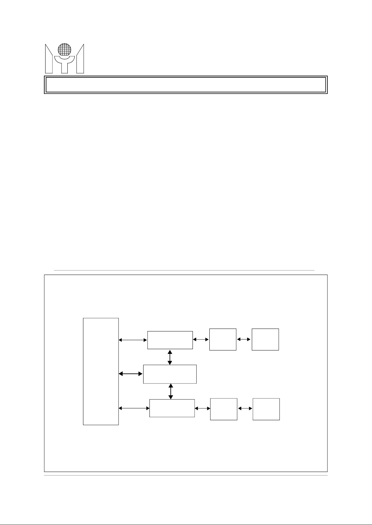
BL OCK DIAGRAM
The MTD502E is a highly integrated, 10M/
100M two port switch controller with build_in
embedded memory. It supports 2 MII/RMII ports
for 10M/100M operation, and both can operate
The MTD502E is an ideal solution for two
port bridge or dual speed hub application, and no
need any external memory buffers in application
design. The flexible MII interface design can
directly connect with pseudo MII interface
The MTD502E provides packet forwarding, address filtering, learning, and aging function, and have an optional back_presure control
address filtering database, which can recognize
up to 2048 MAC addresses. It also support an
automatical aging function for address table
Port0 DMA
Two
Port
Switch
Engine
Port1 DMA
This datasheet contains new product information. Myson Technology reserves the rights to modify the product specification
the product.
1/20 MTD502E Revision 1.3 12/07/2000
MAC0
MAC1
MII0
MII1
f
Page 2
without notice. No liability is assumed as a result of the use of this procuts. No rights under any patent accompany the sales o
TECHNOLOGY
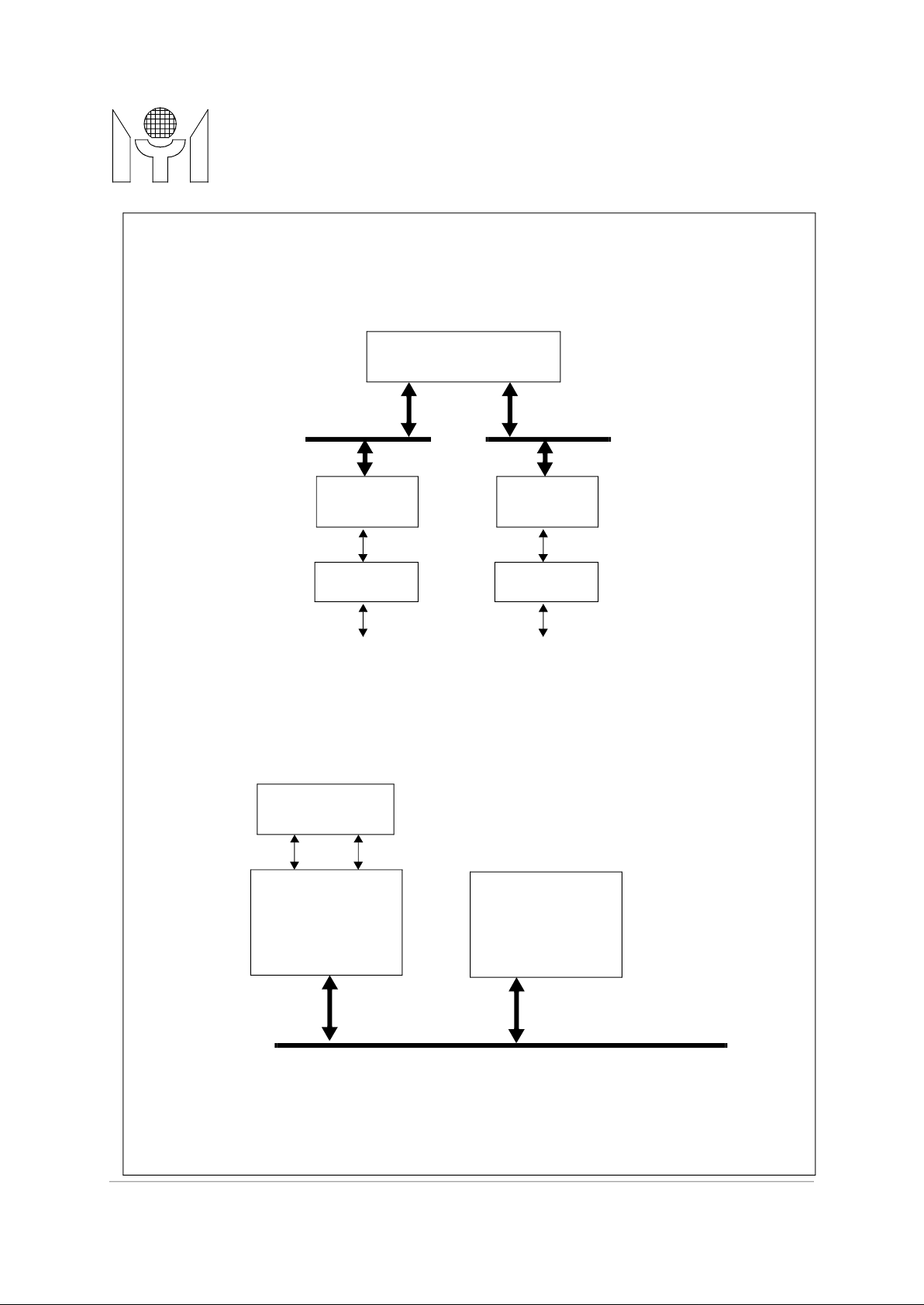
SYSTEM DIAGRAM
2). Dual Speed Hub Appl i c ati on
Transform er
(With out 2P_sw)
1). Two Port Swit c h App l i c atio n (HomePNA to LA N)
MTD502E
MTD502EMYSON
MII1
HomePNA
Transform er
RJ11
MTD502E
MII0
10M/100M
PHYsceiverPHYsceiver
RJ45
10M/100M
Repeater
(With out 2P_sw)
10M/100M
Repeater
.......
Expansion Bus
This datasheet contains new product information. Myson Technology reserves the rights to modify the product specification
the product.E
2/20 MTD502E Revision 1.3 12/07/2000
f
Page 3

MTD502E Revision 1.3 12/07/2000
TECHNOLOGY
MT D502EF
1.0 PIN CONNECTION (under MII mode)
1) 128 Pin PQFP (MTD502EF)
NCNCNCNCLNKRX0_LED
LNKRX1_LED
LNKACT0_LED
LNKACT1_LED
FDCOL0_LED
FDCOL1_LED
GND
COL0_LED
COL1_LEDNCNCNCNCNCNCNCGNDNCNCNCNCNCNCNCGNDNCVCCNCNCNCNC
102
101
10099989796959493929190898887868584838281807978777675747372717069686766
VCC
NC
GND
NC
NC
NC
NC
NC
NC
NC
NC
CLK25OUT
NC
NC
GND
NC
NC
NC
VCC
SYSCLK
GND
NC
NC
NC
NC
RSTB
103
104
105
106
107
108
109
110
111
112
113
114
115
116
117
118
119
120
121
122
123
124
125
126
127
128
VCCNCNC
MTD502EMYSON
65
64
SPEED1
63
COL1
62
CRS1
61
RXDV1
60
GND
59
VCC
58
RXD1_3
57
RXD1_2
56
NC
55
NC
54
NC
53
FULL1
52
RXD1_1
51
RXD1_0
50
NC
49
NC
48
NC
47
RXC1
46
GND
45
VCC
44
NC
43
TXC1
42
TXEN1
41
TXD1_0
40
TXD1_1
39
NC
01020304050607080910111213141516171819202122232425262728293031323334353637
LINK0
TXD0_3
VCC
TXD0_2NCNCNCNC
TXD0_1
TXD0_0
TXEN0
TXC0NCGND
RXC0NCNCNCRXD0_0
RXD0_1
FULL0NCNCNCRXD0_2
RXD0_3
RXDV0
CRS0
COL0
SPEED0
VCC
GND
LINK1
TXD1_3
TXD1_2NCNC
38
NC
3/20
Page 4

MTD502E Revision 1.3 12/07/2000
TECHNOLOGY
NCT
MT D502EG
2) 80 Pin LQFP (MTD502EG)
NCNCLNKRX0_LED
MTD502EMYSON
LNKRX1_LED
LNKACT0_LED
LNKACT1_LED
FDCOL0_LED
FDCOL1_LED
GND
GND
COL0_LED
COL1_LED
GND
GND
GND
GND
VCC
VCC
SPEED1
VCC
NC
VCC
NC
GND
NC
NC
NC
NC
NC
NC
NC
CLK25OUT
VCC
SYSCLK
NC
RSTB
LINK0
TXD0_3
VCC
TXD0_2
60595857565554535251504948474645444342
61
62
63
64
65
66
67
68
69
70
71
72
73
74
75
76
77
78
79
80
01020304050607080910111213141516171819
XD0_1TXD0_0TXEN0TXC0GNDRXC0NCNCNCRXD0_0RXD0_1FULL0NCRXD0_2RXD0_3RXDV0CRS0COL0SPEED0
41
40
COL1
39
CRS1
38
RXDV1
37
GND
36
VCC
35
RXD1_3
34
RXD1_2
33
NC
32
FULL1
31
RXD1_1
30
RXD1_0
29
RXC1
28
TXC1
27
TXEN1
26
TXD1_0
25
TXD1_1
24
NC
23
TXD1_2
22
TXD1_3
21
LINK1
20
4/20
Page 5

MTD502E Revision 1.3 12/07/2000
TECHNOLOGY
Pin 1~32 for Port0, suitable for connecting with 10/
100PHY , RISC_CPU, Switch,....
Pin 33~64 for Port1, suitable for connecting with
HomePNA PHY.
2.0 PIN DESCRIPTIONS
MTD502EF (128PQFP) Pin Defin i t i o n Mappin g Under Diff erent Conf i g u r ati o n s
MTD502EMYSON
Pin No. I/O
1 I LINK0 (NC) LINK0 (NC)
2 O TXD0_3 RXD0_3 (NC) (NC)
3 VCC
4 O TXD0_2 RXD0_2 (NC) (NC)
5 O (NC) CRS0 (NC) (NC)
6~8 I (NC) (NC) (NC) (NC)
9 O TXD0_1 RXD0_1 (NC) (NC)
10 O TXD0_0 RXD0_0 (NC) (NC)
11 O TXEN0 RXDV0 (NC) (NC)
12 I TXC0 (NC) (NC) (NC)
13 I (NC) (NC) (NC) (NC)
14 GND
15 I RXC0 (NC) CRSDV0 TXEN0
16 O (NC) RXC0 TXD0_1 RXD0_1
17 O (NC) COL0 TXD0_0 RXD0_0
18 O (NC) TXC0 TXEN0 CRSDV0
19 I RXD0_0 TXD0_0 RXD0_0 TXD0_0
20 I RXD0_1 TXD0_1 RXD0_1 TXD0_1
21 I FULL0 FULL0 FULL0 (NC)
22~24 O (NC) (NC) (NC) (NC)
25 I RXD0_2 TXD0_2 (NC) (NC)
26 I RXD0_3 TXD0_3 (NC) (NC)
27 I RX DV0 TXEN0 (NC) (NC)
28 I CRS0 SPEED0 SPEED0 (NC)
29 I COL0 (NC) (NC) (NC)
30 I SPEED0 (NC) (NC) (NC)
31 VCC
32 GND
33 I LINK1 (NC) LINK1 (NC)
MII
mode
Phy_MII
mode
Rmii
mode
Phy_Rm
ii mode
Descriptions
34 O TXD1_3 (NC) (NC) (NC)
35 O TXD1_2 (NC) (NC) (NC)
36 O (NC) (NC) (NC) (NC)
37,38 I (NC) (NC) (NC) (NC)
39 I (NC) (NC) CRSDV1 (NC)
40 O TXD1_1 (NC) TXD1_1 (NC)
41 O TXD1_0 (NC) TXD1_0 (NC)
42 O TXEN1 (NC) TXEN1 (NC)
43 I TXC1 (NC) RXD1_0 (NC)
44 I (NC) (NC) RXD1_1 (NC)
45 VCC
5/20
Page 6

MTD502E Revision 1.3 12/07/2000
MTD502EMYSON
Port1: COL LED display, low_active. *
port1’s collision event.
Port0: COL LED display, low_active. *
port0’s collision event.
Port1: FULL/COL LED display, low_active. *
low_active.
TECHNOLOGY
MTD502EF (128PQFP) Pin Defin i t i o n Mappin g Under Diff erent Conf i g u r ati o n s
Pin No. I/O
46 GND
47 I RXC1 (NC) FULL1 (NC)
48~50 O (NC) (NC) (NC) (NC)
51 I RXD1_0 (NC) (NC) (NC)
52 I RXD1_1 (NC) (NC) (NC)
53 I FULL1 (NC) SPEED1 (NC)
54~56 O (NC) (NC) (NC) (NC)
57 I RXD1_2 (NC) (NC) (NC)
58 I RXD1_3 (NC) (NC) (NC)
59 VCC
60 GND
61 I RXD V1 (NC) (NC) (NC)
62 I CRS1 (NC) (NC) (NC)
63 I COL1 (NC) (NC) (NC)
64 I SPEED1 (NC) (NC) (NC)
65~66 I (NC) (NC) (NC) (NC)
67 VCC *
68~71 IO (NC) (NC) (NC) (NC)
72 VCC
73 IO (NC) (NC) (NC) (NC)
74 GND
75,76 IO (NC) (NC) (NC) (NC)
77~79 I (NC) (NC) (NC) (NC)
80 O (NC) (NC) (NC) (NC)
81 IO (NC) (NC) (NC) (NC)
82 GND
83~85 IO (NC) (NC) (NC) (NC)
86~88 I (NC) (NC) (NC) (NC)
89 O (NC) (NC) (NC) (NC)
90 IO Co1_D Co1_D Co1_D Co1_D
MII
mode
Phy_MII
mode
Rmii
mode
Phy_Rm
ii mode
Descriptions
when in half duplex mode: this LED pin present
91 IO Co0_D Co0_D Co0_D Co0_D
92 GND
93 IO FdCo1_D FdCo1_D FdCo1_D FdCo1_D
when in half duplex mode: this LED pin present
when in full duplex mode: this LED pin is always in
when in half duplex mode: this LED pin present
port1’s collision event, using flash style for display.
6/20
Page 7

MTD502E Revision 1.3 12/07/2000
MTD502EMYSON
Port0: FULL/COL LED display, low_active. *
when in full duplex mode: this LED pin is always in
low_active.
Port1: Link_Activity LED display, low_active. *
low_active.
Port0: Link_Activity LED display, low_active. *
low_active.
Port1: Link_Rx LED display, low_active. *
low_active.
Port0: Link_Rx LED display, low_active. *
low_active.
system clock input, 50Mhz operation.
TECHNOLOGY
MTD502EF (128PQFP) Pin Defin i t i o n Mappin g Under Diff erent Conf i g u r ati o n s
Pin No. I/O
94 IO FdCo0_D FdCo0_D FdCo0_D FdCo0_D
95 IO LnAc1_D LnAc1_D LnAc1_D LnAc1_D
96 IO LnAc0_D LnAc0_D LnAc0_D LnAc0_D
97 IO LnRx1_D LnRx1_D LnRx1_D LnRx1_D
MII
mode
Phy_MII
mode
Rmii
mode
Phy_Rm
ii mode
Descriptions
when in half duplex mode: this LED pin present
port0’s collision event, using flash style for display.
when in Link_On state : this LED pin is always in
when have Tx or Rx activity in this port : this LED
pin present port1’s Tx/Rx activity, using flash style
for display.
when in Link_On state : this LED pin is always in
when have Tx or Rx activity in this port : this LED
pin present port0’s Tx/Rx activity, using flash style
for display.
when in Link_On state : this LED pin is always in
when have Rx activity in this port : this LED pin
present port1’s Rx activity, using flash style for display.
98 IO LnRx0_D LnRx0_D LnRx0_D LnRx0_D
when in Link_On state : this LED pin is always in
when have Rx activity in this port : this LED pin
present port0’s Rx activity, using flash style for dis-
play.
99~102 IO (NC) (NC) (NC) (NC)
103 VCC
104 IO (NC) (NC) (NC) (NC)
105 GND
106~110 IO (NC) (NC) (NC) (NC)
111 IO (NC) P0MDIO (NC) P0MDIO
112 IO (NC) P0MDC (NC) P0MDC
113 IO (NC) (NC) (NC) (NC)
114 IO CLK25O CLK25O CLK25O CLK25O clock 25Mhz output.
115~116 IO (NC) (NC) (NC) (NC)
117 GND
118~120 IO (NC) (NC) (NC) (NC)
121 VCC
122 I SYSCLK SYSCLK SYSCLK SYSCLK
123 GND
7/20
Page 8

MTD502E Revision 1.3 12/07/2000
MTD502EMYSON
system resetb input, low_active.
MTD502EF(128PQFP) Jum per Setti ng Table After Power On Reset
Jumper setting function after power on reset.
-external pull_high = 1, means enter 2 port switch mode.
pull_hgih” for well operation.
Jumper setting function after power on reset.
half_duplex) is disabled for two ports both.
P1_Rmii Enable
Jumper setting function after power on reset.
P0_Rmii Enable
Jumper setting function after power on reset.
P0_Phy_Mode Enable
Jumper setting function after power on reset.
-external pull_high = 1, means Port 0 interrface enter PHY mode.
Jumper setting function after power on reset.
limit_4 modified method.
TECHNOLOGY
MTD502EF (128PQFP) Pin Defin i t i o n Mappin g Under Diff erent Conf i g u r ati o n s
Pin No. I/O
124~127 IO (NC) (NC) (NC) (NC)
128 I RSTB RSTB RSTB RSTB
MII
mode
Phy_MII
mode
Rmii
mode
Phy_Rm
ii mode
Descriptions
note: input signal LINK,SPEED,FULL from PHY device are low_active definnition.
Pin No. IO Setting Function Descriptions
5 IO 2P_Sw Enable
-external pull_low = 0, means an internal test mode.
-external floating : default is 0.
For MTD502E application, this pin must always use “external
18 IO Back Pressure Disable
-external pull_high = 1, means back_pressure function ( under
95 IO
97 IO
98 IO
100 IO P1_Bkoff_4 Enable
-external pull_low = 0, means back_pressure function enable.
-external floating : default is 0.
-external pull_high = 1, means Port 1 RMII interface enable..
-external pull_low = 0, means Port 1 is MII interface.
-external floating : default is 0.
-external pull_high = 1, means Port 0 RMII interface enable..
-external pull_low = 0, means Port 0 is MII interface.
-external floating : default is 0.
-external pull_low = 0, means Port 0 interface is using MAC mode.
-external floating : default is 0.
-external pull_high = 1, means Port 1 MAC backoff engine is using
-external pull_low = 0, means Port 1 MAC backoff engine is using
specification defined method.
-external floating : default is 0.
8/20
Page 9

MTD502E Revision 1.3 12/07/2000
TECHNOLOGY
Jumper setting function after power on reset.
limit_4 modified method.
Jumper setting function after power on reset.
-external pull_low = 0.
Jumper setting function after power on reset.
-external pull_low = 0.
Jumper setting function after power on reset.
-external pull_low = 0.
Jumper setting function after power on reset.
-external pull_low = 0.
Jumper setting function after power on reset.
-external pull_low = 0.
Jumper setting function after power on reset.
MTD502EF(128PQFP) Jum per Setti ng Table After Power On Reset
Pin No. IO Setting Function Descriptions
101 IO P0_Bkoff_4 Enable
-external pull_high = 1, means Port 0 MAC backoff engine is using
-external pull_low = 0, means Port 0 MAC backoff engine is using
specification defined method.
-external floating : default is 0.
102 IO DeviceID[4]
-external pull_high = 1.
-external floating : default is 0.
104 IO DeviceID[3]
-external pull_high = 1.
MTD502EMYSON
106 IO DeviceID[2]
107 IO DeviceID[1]
108 IO DeviceID[0]
109 IO P1_CRCchk Disable
-external floating : default is 0.
-external pull_high = 1.
-external floating : default is 0.
-external pull_high = 1.
-external floating : default is 0.
-external pull_high = 1.
-external floating : default is 0.
-external pull_high = 1, means Port1 CRC check and drop function
is disabled.
-external pull_low = 0, means Port1 CRC check and drop function
is enabled.
-external floating : default is 0.
9/20
Page 10

MTD502E Revision 1.3 12/07/2000
TECHNOLOGY
Jumper setting function after power on reset.
Jumper setting function after power on reset.
MTD502EF(128PQFP) Jum per Setti ng Table After Power On Reset
Pin No. IO Setting Function Descriptions
110 IO P0_CRCchk Disable
-external pull_high = 1, means Port0 CRC check and drop function
is disabled.
-external pull_low = 0, means Port0 CRC check and drop function
is enabled.
-external floating : default is 0.
126 IO VLAN tag Enable
-external pull_high = 1, means MAC receiving accept 1522 Bytes
packet (VLAN tag enable).
-external pull_low = 0, means MAC receiving reject 1522 Bytes
packet (VLAN tag disable).
-external floating : default is 0.
MTD502EMYSON
10/20
Page 11

MTD502E Revision 1.3 12/07/2000
TECHNOLOGY
connecting with 10/100PHY ,
RISC_CPU, Switch,....
necting with HomePNA PHY.
3.0 MTD502EG (80LQFP) PIN DESCRIPTIONS
MTD502EG(80LQFP) Pin Defin i t i o n Mappin g Under Diff erent Conf i g u r ati o ns
MTD502EMYSON
Pin No. I/O
1 O (NC) CRS0 (NC) (NC) Pin 77~80, 1~20 for Port0, suitable for
2 O TXD0_1 RXD0_1 (NC) (NC)
3 O TXD0_0 RXD0_0 (NC) (NC)
4 O TXEN0 RXDV0 (NC) (NC)
5 I TXC0 (NC) (NC) (NC)
6 GND
7 I RXC0 (NC) CRSDV0 TXEN0
8 O (NC) RXC0 TXD0_1 RXD0_1
9 O (NC) COL0 TXD0_0 RXD0_0
10 O (NC) TXC0 TXEN0 CRSDV0
11 I RXD0_0 TXD0_0 RXD0_0 TXD0_0
12 I RXD0_1 TXD0_1 RXD0_1 TXD0_1
13 I FULL0 FULL0 FULL0 (NC)
14 O (NC) (NC) (NC) (NC)
15 I RXD0_2 TXD0_2 (NC) (NC)
16 I RXD0_3 TXD0_3 (NC) (NC)
17 I RXDV0 TXEN0 (NC) (NC)
18 I CRS0 SPEED0 SPEED0 (NC)
19 I COL0 (NC) (NC) (NC)
20 I SPEED0 (NC) (NC) (NC)
21 I LINK1 (NC) (NC) (NC) Pin 21~41 for Port1, suitable for con-
MII
mode
Phy_MII
mode
Rmii
mode
Phy_Rm
ii mode
Descriptions
22 O TXD1_3 (NC) (NC) (NC)
23 O TXD1_2 (NC) (NC) (NC)
24 O (NC) (NC) (NC) (NC)
25 O TXD1_1 (NC) (NC) (NC)
26 O TXD1_0 (NC) (NC) (NC)
27 O TXEN1 (NC) (NC) (NC)
28 I TXC1 (NC) (NC) (NC)
29 I RXC1 (NC) (NC) (NC)
30 I RXD1_0 (NC) (NC) (NC)
31 I RXD1_1 (NC) (NC) (NC)
32 I FULL1 (NC) (NC) (NC)
33 O (NC) (NC) (NC) (NC)
34 I RXD1_2 (NC) (NC) (NC)
35 I RXD1_3 (NC) (NC) (NC)
36 VCC
37 GND
38 I RXDV1 (NC) (NC) (NC)
39 I CRS1 (NC) (NC) (NC)
11/20
Page 12

MTD502E Revision 1.3 12/07/2000
MTD502EMYSON
Port1: COL LED display, low_active. *
when in half duplex mode: this LED pin
present port1’s collision event.
Port0: COL LED display, low_active. *
when in half duplex mode: this LED pin
present port0’s collision event.
Port1: FULL/COL LED display,
low_active. *
when in full duplex mode: this LED pin
is always in low_active.
when in half duplex mode: this LED pin
present port1’s collision event, using
Port0: FULL/COL LED display,
low_active. *
when in full duplex mode: this LED pin
is always in low_active.
when in half duplex mode: this LED pin
present port0’s collision event, using
Port1: Link_Activity LED display,
low_active. *
when in Link_On state : this LED pin is
always in low_active.
: this LED pin present port1’s Tx/Rx
activity, using flash style for display.
TECHNOLOGY
MTD502EG(80LQFP) Pin Defin i t i o n Mappin g Under Diff erent Conf i g u r ati o ns
Pin No. I/O
40 I COL1 (NC) (NC) (NC)
41 VCC *
42 I SPEED1 (NC) (NC) (NC)
43 VCC
44 VCC
45 GND
46 GND
47 GND
48 GND
49 IO Co1_D Co1_D Co1_D Co1_D
50 IO Co0_D Co0_D Co0_D Co0_D
51 GND
52 GND
53 IO FdCo1_D FdCo1_D FdCo1_D FdCo1_D
MII
mode
Phy_MII
mode
Rmii
mode
Phy_Rm
ii mode
Descriptions
54 IO FdCo0_D FdCo0_D FdCo0_D FdCo0_D
55 IO LnAc1_D LnAc1_D LnAc1_D LnAc1_D
flash style for display.
flash style for display.
when have Tx or Rx activity in this port
12/20
Page 13

MTD502E Revision 1.3 12/07/2000
MTD502EMYSON
Port0: Link_Activity LED display,
low_active. *
when in Link_On state : this LED pin is
always in low_active.
: this LED pin present port0’s Tx/Rx
activity, using flash style for display.
Port1: Link_Rx LED display,
low_active. *
when in Link_On state : this LED pin is
always in low_active.
LED pin present port1’s Rx activity ,
using flash style for display.
Port0: Link_Rx LED display,
low_active. *
when in Link_On state : this LED pin is
always in low_active.
LED pin present port0’s Rx activity ,
using flash style for display.
system clock input, 50Mhz operation.
system resetb input, low_active.
TECHNOLOGY
MTD502EG(80LQFP) Pin Defin i t i o n Mappin g Under Diff erent Conf i g u r ati o ns
Pin No. I/O
56 IO LnAc0_D LnAc0_D LnAc0_D LnAc0_D
57 IO LnRx1_D LnRx1_D LnRx1_D LnRx1_D
58 IO LnRx0_D LnRx0_D LnRx0_D LnRx0_D
MII
mode
Phy_MII
mode
Rmii
mode
Phy_Rm
ii mode
Descriptions
when have Tx or Rx activity in this port
when have Rx activity in this port : this
when have Rx activity in this port : this
59-61 IO (NC) (NC) (NC) (NC)
62 VCC
63 IO (NC) (NC) (NC) (NC)
64 GND
65-69 IO (NC) (NC) (NC) (NC)
70 IO (NC) P0MDIO (NC) P0MDIO
71 IO (NC) P0MDC (NC) P0MDC
72 O CLK25O CLK25O CLK25O CLK25O clock 25Mhz output.
73 VCC
74 I SYSCLK SYSCLK SYSCLK SYSCLK
75 IO (NC) (NC) (NC) (NC)
76 I RSTB RSTB RSTB RSTB
77 I LINK0 (NC) LINK0 (NC)
78 O TXD0_3 RXD0_3 (NC) (NC)
79 VCC
80 O TXD0_2 RXD0_2 (NC) (NC)
note: input signal LINK,SPEED,FULL from PHY device are low_active definnition.
13/20
Page 14

MTD502E Revision 1.3 12/07/2000
TECHNOLOGY
MTD502EG(80LQFP) Jumper Sett i ng Table Af ter Power On Reset
Jumper setting function after power on reset.
-external pull_high = 1, means enter 2 port switch mode.
pull_hgih” for well operation.
Jumper setting function after power on reset.
half_duplex) is disabled for two ports both.
P0_Rmii Enable
Jumper setting function after power on reset.
P0_Phy_Mode Enable
Jumper setting function after power on reset.
-external pull_high = 1, means Port 0 interrface enter PHY mode.
Jumper setting function after power on reset.
limit_4 modified method.
Jumper setting function after power on reset.
limit_4 modified method.
Jumper setting function after power on reset.
-external pull_low = 0.
Pin No. IO Setting Function Descriptions
1 IO 2P_Sw Enable
-external pull_low = 0, means an internal test mode.
-external floating : default is 0.
For MTD502E application, this pin must always use “external
10 IO Back Pressure Disable
-external pull_high = 1, means back_pressure function ( under
-external pull_low = 0, means back_pressure function enable.
-external floating : default is 0.
57 IO
-external pull_high = 1, means Port 0 RMII interface enable..
-external pull_low = 0, means Port 0 is MII interface.
-external floating : default is 0.
58 IO
MTD502EMYSON
59 IO P1_Bkoff_4 Enable
60 IO P0_Bkoff_4 Enable
61 IO DeviceID[4]
-external pull_low = 0, means Port 0 interface is using MAC mode.
-external floating : default is 0.
-external pull_high = 1, means Port 1 MAC backoff engine is using
-external pull_low = 0, means Port 1 MAC backoff engine is using
specification defined method.
-external floating : default is 0.
-external pull_high = 1, means Port 0 MAC backoff engine is using
-external pull_low = 0, means Port 0 MAC backoff engine is using
specification defined method.
-external floating : default is 0.
-external pull_high = 1.
-external floating : default is 0.
14/20
Page 15

MTD502E Revision 1.3 12/07/2000
TECHNOLOGY
Jumper setting function after power on reset.
-external pull_low = 0.
Jumper setting function after power on reset.
-external pull_low = 0.
Jumper setting function after power on reset.
-external pull_low = 0.
Jumper setting function after power on reset.
-external pull_low = 0.
Jumper setting function after power on reset.
Jumper setting function after power on reset.
Jumper setting function after power on reset.
MTD502EG(80LQFP) Jumper Sett i ng Table Af ter Power On Reset
Pin No. IO Setting Function Descriptions
63 IO DeviceID[3]
-external pull_high = 1.
-external floating : default is 0.
65 IO DeviceID[2]
-external pull_high = 1.
-external floating : default is 0.
66 IO DeviceID[1]
-external pull_high = 1.
-external floating : default is 0.
67 IO DeviceID[0]
-external pull_high = 1.
MTD502EMYSON
68 IO P1_CRCchk Disable
69 IO P0_CRCchk Disable
71 IO VLAN tag Enable
-external floating : default is 0.
-external pull_high = 1, means Port1 CRC check and drop function
is disabled.
-external pull_low = 0, means Port1 CRC check and drop function
is enabled.
-external floating : default is 0.
-external pull_high = 1, means Port0 CRC check and drop function
is disabled.
-external pull_low = 0, means Port0 CRC check and drop function
is enabled.
-external floating : default is 0.
-external pull_high = 1, means MAC receiving accept 1522 Bytes
packet (VLAN tag enable).
-external pull_low = 0, means MAC receiving reject 1522 Bytes
packet (VLAN tag disable).
-external floating : default is 0.
15/20
Page 16

MTD502E Revision 1.3 12/07/2000
MTD502EMYSON
4.0 FUNCTIONAL DESCRIPTIONS
The MTD502E implements a 10/100M two port switch for 10M/100M packet switching. Total 2K
packet to port1.
The address entries are scheduled in the aging machine. If one station does not transmit any packet for
time value is 300 seconds.
used to show the corresponding memory address for each incoming packet. In addition, the buffer
achieve the predefined threshold value, the buffer queue manager will raise the alarm signal which is
used to enable the flow control mechanism for avoiding transmission ID queue overflow happening.
ping packets. If the “back pressure control disable” bit is set, and there is no free buffer queue available
4.5 MAC and DMA eng i ne
frame stripping, CRC checking, bad packet dropping, defering to line traffic, and collision handling. The
The MAC Tx_engine will constantly monitor the line traffic using derfering precedure. Only if it has been
TECHNOLOGY
address entrys are provided for packets’ SA learning and DA routing; and also provide automatic aging
function ( aging time = 300secs). When using in two port bridge application, the input packets from
port0 will be stored in an embedded memory buffers of MTD502E first, while packets is good for forwarding ( CRC chech ok, 64Bytes < length > 1518Bytes, and not local packets ) , than forward this
4.1 L earni ng and Routi ng
The MTD502E supports 2K MAC entries for filtering. Dynamic address learning is performed by each
good unicast packet is completely received. The routing process is performed whenever the packet’s
DA is captured. If the DA get a hit result in self port’s address table, this packet will be treated as a “
local packet”, and then drop the packet forwarding to the other port. On the other hand, if this packet is
not a “local packet”, then will be forwarded to the other port.
4.2 Agin g
a period of time, the belonging MAC address will be kicked out from the address table. The aging out
4.3 Buff er Queue Management
The buffer queue manager is implemented to manage the embedded memory packet buffering. The
main function of the buffer queue manager is to maintain the linked list consists of buffer IDs, which is
queue manager monitors the rested free spaces status of the memory buffers, If the packet storage
MTD502E provide back pressure control scheme in half duplex mode.
4.4 Half Dupl ex Back Pressu r e Contro l
In half duplex mode, MTD502E provide a back pressure control mechanism to avoid dropping packets
during network conjection situation. When the “back pressure control enable” bit is set during power on
reset (pin_18 is external pull_low), it enables MTD502E supporting back pressure function in
half_duplex mode; When output port buffer queue’s on_using value reach the initialization setting
threshold value, MTD502E will send a JAM pattern in the input port when it senses an incoming packet
, thus force a collision to inform the remote node transmission back off and will effectively avoid drop-
for the incoming packets, the incoming packets will be dropped.
The MTD502E’s MAC performs all the functions in IEEE802.3 protocol, such as frame formatting,
MAC Rx_engine checks incoming packets and drops the bad packet which include CRC erro r, align-
ment error, short packet (less than 64 bytes), and long packet(more than 1518 bytes or 1522 bytes
when the “VLAN tag 1522 bytes receive enable” bit is set during power on reset). Before transmission,
idle for a 96 bits time (a minimum interpacket gap time, IPG time), actual transmmission can be started.
For the half duplex mode, MAc engine will detect collision; if a collision is detected, the MAC Tx_engine
will transmit a JAM pattern and then delay the re_transmission for a random time period determined by
the back_off algorithm (MTD502E implements the truncated exponential back_off algorithm defined in
IEEE 802.3 standard). For the full duplex mode, collision signal is ignored.
16/20
Page 17

MTD502E Revision 1.3 12/07/2000
MTD502EMYSON
5.1 Abso lu te Maximum Rating s
Power Supply Voltage
Storage Temperature
Industrial Junction Operating Temperature
Tri-state Leakage Current
Bi-direction buffer Capacitance
Input High Voltage
Output High Voltage
Output Low Voltage
TECHNOLOGY
5.0 Electri c al Characteri st i c s
Symbol Parameter RATING Unit
V
CC
V
T
V
OUT
STG
Input Voltage -0.3 to Vcc+0.3 V
IN
Output Voltage -0.3 to Vcc+0.3 V
5.2 Recom mend ed Operatin g Condi ti on s
Symbol Parameter Min. Typ. Max. Unit
V
V
Power Supply 3.0 3.3 3.6 V
CC
Input Voltage 0 - Vcc V
IN
Commercial Junction Operating Temperature 0 25 115
T
j
-0.3 to 3.6 V
-55 to 150
ο
-40 25 125
C
ο
ο
C
C
5.3 DC Electr i c al Characteris t ic s
Symbol Parameter Conditions Min. Typ. Max. Unit
I
I
C
C
OUT
C
BID3
V
V
V
V
R
(Under recommended operating conditions and Vcc = 3.0 ~ 3.6V, Tj = 0 to +115 oC)
Input Leakage Current no pull-up or down -1 1 uA
IL
OZ
Input Capacitance 2.8 pF
IN
-1 1 uA
Output Capacitance 2.7 4.9 pF
2.7 4.9 pF
Input Low Voltage CMOS 0.3*Vcc V
IL
IH
OH
OL
Input Pull-up/down resistance
I
IOL=2,4,8,12,16,24mA
IOH=2,4,8,12,16,24mA
CMOS 0.7*Vcc V
2.4 V
VIL=0V or VIH=V
CC
75 KOhm
0.4 V
17/20
Page 18

MTD502E Revision 1.3 12/07/2000
TECHNOLOGY
FIG URE 1. MII timing
FIG URE 2. RMII timing
5.4 Electr ic al Characteristi c s
MTD502EMYSON
RXCLK0
CRS0/RXDV0
RXD0[3:0]
TXCLK0
TXEN0
TXD0[3:0]
Symbol Parameter Min. Typ. Max. Unit Note
T5 MII input setup time 10 nS
T6 MII input hold time 10 nS
T7 MII output setup time 3 nS
T8 MII output hold time 5 nS
T5
T7
T6
Valid
T8
Valid
REFCLK
CRSDV
RXD[1:0]
TXEN
TXD[1:0]
Symbol Parameter Min. Typ. Max. Unit Note
T1 RMII input setup time 1 nS
T2 RMII input hold time 1 nS
T3 RMII output setup time 3 nS
T4 RMII output hold time 5 nS
T1
T3
T2
Valid
T4
Valid
18/20
Page 19

MTD502E Revision 1.3 12/07/2000
TECHNOLOGY
1.Dimension D1 & E1 do not include mold protrusion.
3.Controlling dimension : Millimeter.
6.0 128 pin PQFP Package Data
D
1
D
65102
103
128
1 38
y
Seating Plane
See Detail A
e
B
See Detail B
64
39
MTD502EMYSON
Dimension in inch Dimension in mm
Symbol
Min Norm Max Min Norm Max
A - - 0.134 - - 3.40
A1 0.010 - - 0.25 - A2 0.107 0.112 0.117 2.73 2.85 2.97
B 0.007 0.009 0.011 0.17 0.22 0.27
C 0.004 - 0.008 0.09 - 0.20
D 0.906 0.913 0.921 23.00 23.20 23.40
D
0.783 0.787 0.791 19.90 20.00 20.10
1
1
E
E
A
A1 A2
B
E 0.669 0.677 0.685 17.00 17.20 17.40
E
0.547 0.551 0.555 13.90 14.00 14.10
1
e 0.020 BSC 0.50 BSC
L 0.029 0.035 0.041 0.73 0.88 1.03
L1 0.063 BSC 1.60 BSC
y - - 0.004 - - 0.10
o
z
Note:
But mold mismatch is included. Allowable protrusion is .25mm/.010” per side.
2.Dimension B does not include dambar protrusion. Allowable dambar protrusion .08mm/.003”. Total in excess of the B dimemsion at maximum material
condition. Dambar cannot be located on the lower radius or the foot.
-
0
7o0
o
o
-
7
Gage Plane
L
With Plating
C
z
Base Metal
L1
Detail A
Detail B
19/20
Page 20

MTD502E Revision 1.3 12/07/2000
TECHNOLOGY
7.0 80 pin LQFP Packag e Data
D
D
1
R
2
Gage Plane
60
61
80
1
e
See Detail A
Seating Plane
R
1
L
L1
Detail A
41
40
20
b
See Detail B
MTD502EMYSON
Dimension in inch Dimension in mm
Symbol
Min Norm Max Min Norm Max
A - - 0.063 - - 1.60
A1 0.002 - 0.006 0.05 - 0.15
A2 0.053 0.055 0.057 1.35 1.4 1.45
b 0.007 0.009 0.011 0.17 0.22 0.27
b
0.007 0.008 0.009 0.17 0.20 0.23
1
C 0.004 - 0.008 0.09 - 0.20
C
1
E
E
21
A
A1 A2
b
b
1
1
C
C
Detail B
With Plating
Base Metal
0.004 - 0.006 0.09 - 0.16
1
D 0.551 BSC 14.00 BSC
D
E 0.551 BSC 14.00 BSC
E
e 0.020 BSC 0.50 BSC
L 0.018 0.024 0.030 0.45 0.60 0.75
L
R
R
0.472 BSC 12.00 BSC
1
0.472 BSC 12.00 BSC
1
0.039 REF 1.00 REF
1
0.003 - - 0.08 - -
1
0.003 - 0.008 0.08 - 0.2
2
20/20
 Loading...