

Page 1
MYSON
TECHNOLOGY
MTD492
Coaxial Transceiver Interface
This datasheet contains new product information. Myson Technology reserves the rights to modify the product specification without notice. No
liability is assumed as a result of the use of this product. No rights under any patent accompany the sale of the product.
MTD492 Revision 3.5 01/07/1997
1/8
FEATURES
•
Compatible with IEEE 802.3 10Base5 (Ethernet) and 10Base2 (Cheapernet).
• Internal A UI squelch circuitry for noise rejection.
• Transmission I DL detection at end of packet and dri bble bit rej ec tion window.
• Reception dribble bit rejection window.
• Reception and tr ansmission mode collision detection.
• Extended collision detection to turn off receiving path.
• CD heartbeat ex ternally controllabl e.
• Advanc ed low-power, high-perfor mance CMOS tec hnology.
• ESD protection greater than 2000 Volts.
•
16-pin PDIP and 28- pin PLCC packages.
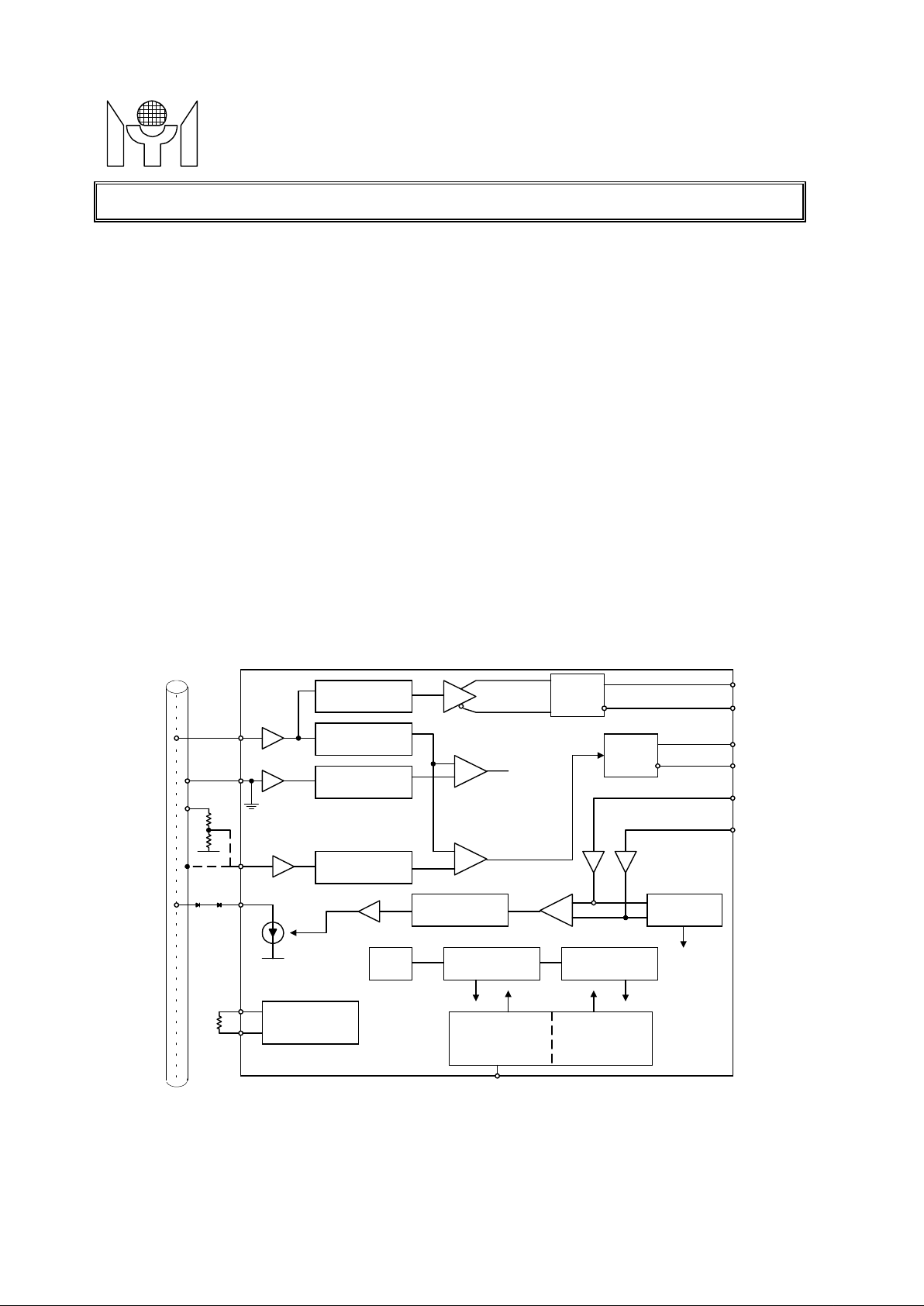
GENERAL DESCRIPTION
The MTD492 transceiver integrates the coax ial cable interface functions of the Medium Attachm ent Unit
(MAU) in Ethernet or Cheapernet LAN applications. I n an Et hernet 10Base5 network, MTD492 is mounted
on the thick E thernet coaxial cable and connects to a station through an AUI cable. For Cheaper net
applicat ions, MTD492 is connected to the Cheapernet coax ial cable t hr ough a B NC c onnec tor and is
usually m ounted on the LAN adapter in a station.
BLOCK DIAGRAM
HIGH PASS
EQUALIZATION
LOW PASS
FILTER
LOW PASS
FILTER
COM
-
+
LOW PASS
FILTER
125
10K
REFERENCE
CIRCUIT
1K
AUI
DRIVER
AUI
DRIVER
CARRIER
SENSE
-
+
WAVEFORM
SHAPING
+
-
DC/AC
SQUELCH
WATCH DOG
TIMER 26ms
JABBER RESET
TIMER 0.4sec
10MHz
OSC
TRANSMIT
STATE
MACHINE
RECEIVE
STATE
MACHINE
XMTSQ
CLK
VEE
COLLISION
HBE
FXI
GND
COAX
VEE
XMT
CDS
RECV
TXO
RR+
RR-
RX+
RX-
CD+
CD-
TX+
TX-
Page 2
MYSON
TECHNOLOGY
MTD492
MTD492 Revision 3.5 01/07/1997
2/8
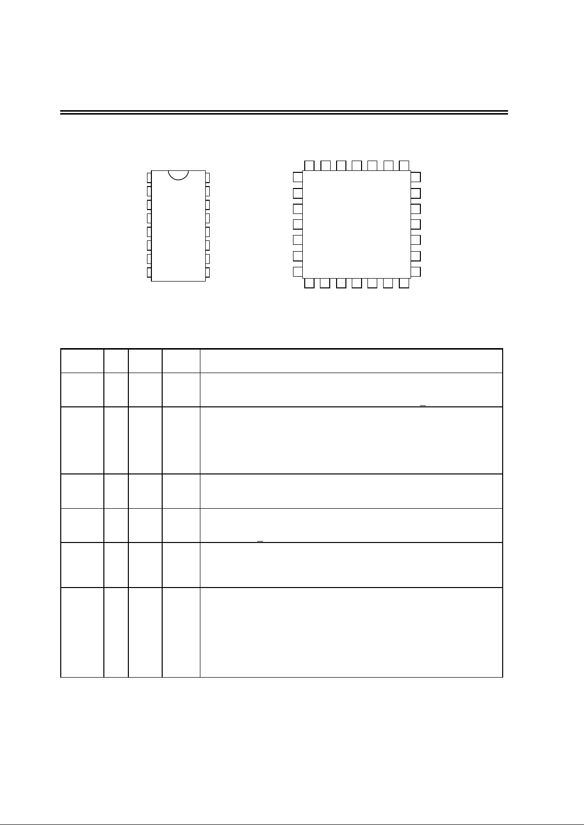
1.0 CONNECTION DIAGRAM
MTD492N
16 PIN PDIP
MTD492V
28 PIN PLCC
CD+
CD-
RX+
VEE
VEE
RX-
TX+
TX-
CDS
TX0
RXI
VEE
RRRR+
GND
HBE
VEE
VEE
VEE
VEE
VEE(NC)
VEE(NC)
VEE(NC)
RX+
CD-
CD+
CDS
TXDNCRXI
VEE(NC)
VEE
VEE
VEE
VEE
VEE(NC)
RR-
RX-
TX+
TX-
HBE
GND
GND
RR+
1
2
3
4
5
6
7
8
24
23
22
21
20
19
18
17
2.0 PIN DESCRIPTIONS
Name I/O PDIP
Pin#
PLCC
Pin#
Description
TX+,TX- I 7,8 13,14
Transmission Data Input.
A balanced differential line receiver which
receives inputs from the off-chip Manchester Code Converter(MCC) t o
the Transmitter. The c ommon m ode volt age on TX+ is set internally .
HBE I 9 15
Heartbeat Enab ler.
The CD heartbeat t est is enabled when HBE is
connected to Ground and di sabled when HBE is connected t o VEE.
This pin is i nternally biased at 0.5 VEE. Test mode i s enabl ed if thi s
pin is left floating or bi ased i n the range of -3.5V to -5.5V. Jabber is
disabled in t est mode. Exiting the jabber disable mode r equires at
least jabber reset time.
RR+,RR- I 11,12 18,19
External Resist or.
A 1kΩ/1% resistor should be connected across
these pins to correct ly set internal operating currents. RR+ is
internal ly shorted to GND.
RXI I 14 26
Network Receiving Input.
Should be connected to the COAX center
conductor. Signals meeting receiver squelch li mits are recovered and
output on RX+. RXI also detects the collision voltage level .
CDS I 16 1
Collision Detection Sense.
Connects directly to the COAX
shield, providing a reference for the collision detection voltage
level for r ec eption-mode det ec tion. An ex ternal bias network can be
used to shift the detection t hr eshol d for transmission-detection mode.
CD+,CD- O 1,2 2,3
Collision Output.
A balanced differential line driver drives this
output pair from the collision detection circuitry. A 10MHz signal from
the internal oscillator is transferred to these outputs in the event of
collision, excessive transmission (jabber), or duri ng hear tbeat
conditi on. These outputs are open sources, and pull- down resistors of
510Ω to VEE are required. To minimize power dissipation, both open
source outputs are disabled during idle condition, al lowing the
common mode on the pull- down resistors to be pulled to VEE.
Page 3
MYSON
TECHNOLOGY
MTD492
MTD492 Revision 3.5 01/07/1997
3/8
RX+,RX- O 3,6 4,12
Reception Data Output.
A balanced differential output dr ives the
data
recov er ed from t he network to the MCC. These output s are also open
sources, and pull-down resistors of 510Ω to VEE are required. These
pins are biased at -2V during idle time. When an ext ended per iod of
collision condition happens, the receiving path is di sabl ed. Any
interruption of collision will re-enable the receivi ng path.
TXO O 15 28
Transmission Output.
Should be connected to the coaxi al cable via
either one (Cheapernet) or 2 serial i sol ation diodes (Ethernet).
GND 10 17
Positive Supply Pin(Ground).
Should be connected to the COAX
shield.
VEE 4,5,135, 6, 7,
8, 9, 10,
11, 20,
21, 22,
23, 24,
25
Negative Power Supply.
-9 Volts. A 0.1µF decoupli ng c apac itor
must be connected across GND and VEE as close to the device as
possible.
3.0 FUNCTIONAL DESCRIPTIONS
3.1. Transmission Path
The transmission data is input from TX+/ - pins differentially. In general, this differential signal is coupled
through an AUI i sol ation transfor mer. In the M A U desi gn, it is preferable that an equivalent 78 Ohm load be
placed across these 2 pins for pr oper loading for the signal source. Improper load terminati on may cause
excess undershoot at the end of the packet, whic h c auses the dribble bit t o be transmitt ed er r oneousl y .
The transmission signal is first checked against t he on- c hip DC/AC squelch condi tion. If the signal i s
greater than the squel c h threshold (-175 to -300 mV) and the width is wider t han 17 nsec, the squelch is
turned off. The squelch r emains off until the DC squelch condition is not met or an end- of-packet I DL is
detected (at the end of the packet, data remains at 1 for l onger than 175 nsec). Once IDL i s detec ted,
MTD492 provides a 0.8 usec reject ion window that prev ents dribble bit transmission at the A UI interface.
When the squelch is off, the transmission path is enabled and dat a is fed into a waveform shaping circuit
followed by the transmission out put buff er . The waveform shaping function contr ols the output rise/fall time
between 20nsec and 30 nsec, and mini mizes the m ismatch between the rise/fall time. MTD492 provides a
current source output that should be connected to the coaxial cable through at least one isolati on diode.
When data is high, the out put current is virtually zero (ther e is approximately less than 1mA output in t his
state to maintain the linearity of the output buffer) ; when data is low, the output cur r ent peaks at around 80
mA. T his provi des an approximat e 2V peak to peak swing on a 25 Ohm load. Due to the nature of
Manchester code, the average output DC c ur r ent is half of the peak - 40 mA, i.e. 1V DC average on the
cable 25 Ohm load.
3.2. Reception Path
The signal on the c oaxial cable is fi r st buffered. The DC aver age of the signal is extracted by a low pass
filter. When the DC average exceeds the carrier sense threshold (Vcs), the reception data path is turned
on. The signal goes thr ough a high pass filt er for equali z ation of high frequency loss on the cable and then
is compared wit h its center value. The comparator output is amplified by the A UI driver to provide adequate
driving for the RX+/- output.
The end of t he pac k et is determined by 2 conditi ons. If the received dat a is high longer than 175nsec or t he
DC average does not meet the carrier sense threshold, the recept ion data path is turned off. M TD492 then
appends the IDL pulse to the end of the packet. A r ejection window of 1 usec t hat blocks the data reception
path is also turned on.
Page 4

MYSON
TECHNOLOGY
MTD492
MTD492 Revision 3.5 01/07/1997
4/8
The RX+/- output pin is driven by a source follower. Therefore, an ext er nal pull-down load is required for
these 2 pins. During idle state, RX+/- is biased at around -1.5V.
Page 5

MYSON
TECHNOLOGY
MTD492
MTD492 Revision 3.5 01/07/1997
5/8
3.3. Collision Detection Path
In 10Base2 and 10Base5, a collision condition i s deter mined by the DC level on the cable. The DC average
is extracted by a low pass filter. The output of the filter is compared with an internally set threshold (Vcd) to
determine the collision condition. The i nternal threshold is set for the recept ion-collision mode. By
definition, MTD492 will detect collision conditions caused by more than 2 stations simultaneously
transmitting.
The collision detection threshold can be shifted by applying a voltage to the CDS pi n. This is typi c ally done
by a resistor divider network between GND and VEE to implement the t ransmission-collision mode
detection. Transmission-collision differs from reception-collision in that transmission-collision will only
detect a 2-station collision if it is transmitting.
Once a collision is detected, MTD492 turns on the CD+/- pi ns. These 2 pins are also driven by source
followers, thus requiring external pull-down resistors. However, the followers are disabled during idle time,
and CD+/- will be pulled down to VEE and no current will flow through the external r esi stor s.
Because Vcd is always larger t han V c s, when a collision occurs the reception path will also be turned on.
MTD492 implements an i nternal timer of 250 msec to detect the extended collision period. When a collision
conditi on per iod extends beyond this timer, the reception path is turned off. Any int er r uption of t he c ollision
will reset the timer.
3.4. Reference an d Control
The internal reference of MTD492 is generat ed by an on- c hip bandgap circui t. An exter nal resistor
connected between RR+ and RR- pi ns i s used to set the r eference current level. Typic ally, a precision 1K
Ohm resistor shoul d be used. RR+ is internal ly shorted to GND, while RR- is biased at around -1.25V.
The heartbeat and jabber functions of MTD492 are implemented in the tr ansmission state machine. The
heartbeat function is cont r olled by the HBE pin. MTD492 also provides a test mode that disables the jabber
function also controlled by the HBE pin. HBE has a 3-level input. It is biased inter nally at around -4.5V
(0.5Vee). When HBE i s pul led high by a low value resistor (<4.7K), the heartbeat funct ion is enabled; when
it is pul led low, the heartbeat is disabled. If it is driven to the mid-level or left floati ng, the jabber is di sabl ed.
The exi t of the j abber disable state takes about 0.5 sec (jabber reset time).
4.0 ABSOLUTE MAXIMUM RATIN GS
DC Supply Voltage(VEE) -12V
Input Voltage GND+0.3 to VEE-0. 3V
Storage Temperature -65
o
to 150oC
Ambient Operating T emperature 0
o
to 70oC
ESD Protect ion except for Pin14 2000V
Page 6

MYSON
TECHNOLOGY
MTD492
MTD492 Revision 3.5 01/07/1997
6/8
5.0 ELECTRICAL CHARACTERISTICS
(under operating c onditions) (Note 1)
OPERATING CONDITIONS
DC Supply Voltage (VEE) 8.55-9.45V
Operating Temperature 0
o
to 70oC
Parameter Symbol Min Typ Max Unit
Recomm ended S upply Voltage VEE -8. 55 -9. 0 -9.45 V
Supply Current (all VEE pins) Non-transmission IEEidle - -25 -35 m A
Transmission IEExmt - -70 -80 mA
Receiver Input Bi as Current (RXI) Irxi -2 - +25
µ
A
Transmission O utput DC Current (TXO) Itdc 37 41 45 mA
Transmission O utput AC Current (T XO) Itac +28 - Itdc mA
Collision Threshold (Reception Mode) Vcd -1.45 -1.53 -1.62 V
Carrier Sense Threshol d ( RXI) Vcs -0.38 -0.45 -0.52 V
Differential Output Voltage (RX+,CD+) Vod +500 - +1500 mV
DC Common M ode Output Volt age ( RX+) Vocrx -1.0 -2.0 -3.0 V
DC Common M ode Output Volt age ( CD+) (Note 2) Voccd VEE VEE VEE V
Idle State Differential Offset Voltage(RX+,CD+) Vob - 0 +40 mV
Transmission Squelch Threshold(TX+) ( Note 3) Vts -175 -225 -300 m V
Input Capacitance (RXI) Cx - 1.5 - pF
Shunt Resistance - Non-t r ansmission Rrxi 100 - -
k
Ω
Shunt Resistance - Tr ansmission Rtxo 10 - -
k
Ω
Notes: 1. Testi ng is done under the testing l oad defined in Figure 6.
2. During an idle condition, Voc is pulled down to VEE to mi nim ize the power dissipati on across the
load resistors connected to CD+pins.
3. Tested under continuous 5MHz wavef or m that represents the preamble.
6.0 SWITCHING CHARACTERISTICS
(under operating c onditions) (Note 1)
Parameter Symbol M in Typ M ax Unit
Reception St ar t-up Delay (RXI to RX+) Tron - 2.5 5 bits
Reception Propagation Delay (RXI t o RX+) Trd - 35 50 ns
Differential Output Ri se Time (RX+,CD+ ) Trr - 4 7 ns
Differential Output Fall Time (RX+,CD+) Trf - 4 7 ns
Receiver and Cable Total Jitter Trj - +2 -ns
Transmission Start-up Delay Ttst - 1 2 bits
Transmission Pr opagation Delay Ttd - 25 50 ns
Transmission Rise Time (10%-90%) ( TXO) Ttr 20 25 30 ns
Transmission F all Time (10%-90%) (TXO) Ttf 20 25 30 ns
Ttr and Trf Mismatch Ttm - +0.5 +3.0 ns
Transmission Skew(TXO) Tts - +0.5 +2 ns
Transmission T ur n- on P ulse Wi dth at Vts(TX+) (Not e 4) Tton 10 20 40 ns
Transmission T ur n- off Delay Ttof f 130 200 260 ns
Transmission I DL Detection Time (Note 5) Ttidl 130 170 200 ns
Collision Turn-on Delay Tcon - 7 13 bits
Collision Turn-off Delay Tcoff - - 20 bits
Page 7

MYSON
TECHNOLOGY
MTD492
MTD492 Revision 3.5 01/07/1997
7/8
Collision Frequency (CD+) Fcp 8.5 10 12.5 MHz
Collision Pulse Width (CD+) Tcp 405060 ns
Extended Collision Detection Time (Note 6) Tcxd 100 200 300 ms
CD Heartbeat Delay ( TX+ to CD+) Thon 0.6 1.1 1.6
µ
s
CD Heartbeat Duration(CD+) Thw 0.5 1.0 1.5
µ
s
Jabber Acti vati on Delay(TX+ to CD+) Tja 202632ms
Jabber Reset Time-out (TX+ to TXO and CD+) Tjr 300 420 550 ms
Notes: 4. For a minimum pulse amplit ude of > -300 m V .
5. IDL detection precedes the t r ansmission turn-off by transmission propagation delay.
6. Time needed to detec t an extended peri od of collision in order to turn off the reception path.
7.0 TIMING DIAGRAM
INPUT
TO RXI
RX+
RX-
T
ron
50%
50%
T
rd
90%
10%
T
rf
T
rr
T
roff
Figure 1. Rec eption Timing
TX+
TX-
TXO
OUTPUT
T
tst
T
toff
T
tidl
V
ts
T
ton
T
td
T
tf
T
tr
50%
50%
90%
10%
Figure 2. Transmission Ti ming
T
hon
T
hw
TX+
TX-
CD+
CD-
Figure 3. Hear tbeat Timing
Vcd (min)
T
con
Vcd (max)
-1.75V
0V
-6.8V
-1.2V
T
coff
1/F
cp
T
cp
INPUT
to RXI
CD+
CD-
Figure 4. Collision Timing
Page 8

MYSON
TECHNOLOGY
MTD492
MTD492 Revision 3.5 01/07/1997
8/8
TX+
TX-
TXO
CD+
CD-
T
ja
T
jr
Figure 5. J abber Timi ng
25
Ω
TXO
Transmitter
Output
39
Ω
510
Ω
50µH*
39
Ω
510
Ω
VEE
Receiver (RX )
Collision(CD )
Outputs
+
-
+
-
*: 50µH inductor is used for testing purposes. Pul se tr ansformers with hi gher pr imary i nduc tance are
recommended.
Figure 6. Test Loads
8.0 PACKAGE DIMENSION
75+/-20
90+/-20
R40
55+/-20
312+/-12 100+/-20
250+/-4
350+/-20
10
18+/-2Typ 60+/-5Typ
15Min.
15Max
115Min
15Max
100Typ
35+/-5
7Typ
750+/-10
60+/-4
60+/-4
310Max
 Loading...