

Page 1
MYSON
This datasheet contains new product information. Myson Technology reserves the rights to modify the product specification without notice.
is built for easy MAU interface in a coaxial Ethernet network. The MTD392 product family integrates the coaxial
Cheapernet LAN applications. In an
MTD393 applications with enhanced
MTD392
TECHNOLOGY
FAMILY
Coaxial Transceiver Interface
FEATURES
· Compatible with ISO/IEEE 802.3 10Base5 (Ethernet) and 10Base2 (Cheapernet).
· Functionally compatible with National DP8392C.
· Internal squelch circuitry for noise rejection.
· Reception/transmission mode collision detection.
· Transceiver functions integrated except for signal and power isolation.
· CD heartbeat externally selectable.
· Advanced low-power, high-performance CMOS technology.
· ESD protection greater than 2000 volts.
· 16-pin plastic DIP package, 24-pin skinny plastic DIP package, or 20 and 28-pin PLCC packages.
· Built-in LED drivers for collision, reception, jabber and transmission status display (MTDX93/X94 only).
· Collision detection mode for reception, transmission and hybrid (MTDX94 only).
· Special test mode allowing continuous transmission for waveform testing (MTDX94 only).
GENERAL DESCRIPTION
The MTD392 family includes a series of products, MTD392/3/4 and MTD492/3/4. The MTD392 product family
cable interface functions of Medium Attachment Unit (MAU) in Ethernet or
Ethernet 10Base5 network, the MTD392 product family is mounted on the thick Ethernet coaxial cable and
connects to a station through an AUI cable. For Cheapernet applications, the MTD392 product family is
connected to the Cheapernet coaxial cable through a BNC connector and is usually mounted on the LAN
adapter in a station.
Following is a table describing the differences among the MTD392 product family:
Product Features
MTD392 Basic transceiver 16-PDIP
MTD393 MTD392 with built-in LEDs 20-PLCC
MTD394 MTD393 with enhanced collision
detection mode, special pin for
testing
MTD49X MTD39X with improved
performance
Package
Types
28-PLCC
24-PDIP
24-PDIP
28-PLCC
Recommended Applications
Adapter boards
Adapter cards with status LEDs
collision detection
Basic MTD39X applications, Hub,
repeater and MAU applications
No liability is assumed as a result of the use of this product. No rights under any patent accompany the sale of the product.
1/10
MTD392 Revision 2.01 02/25/1997
Page 2
MYSON
MTD392
TECHNOLOGY
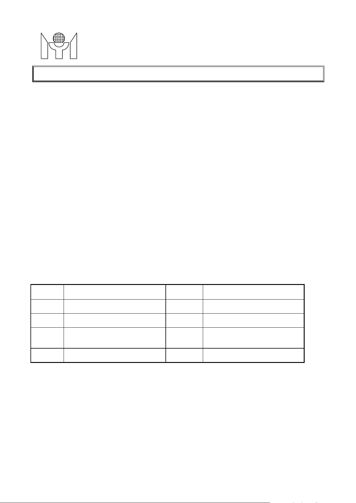
BLOCK DIAGRAM FOR MTD392 FAMILY
COAX
125
10K
VEE
RECV
1K
FXI
GND
XMT
CDS
TXO
VEE
RR+
REFERENCE
RR-
EQUALIZATION
CIRCUIT
HIGH PASS
LOW PASS
FILTER
LOW PASS
FILTER
LOW PASS
FILTER
10MHz
OSC
WAVEFORM
CLK
COM
-
+
-
+
SHAPING
WATCH DOG
TIMER 26ms
TRANSMIT
MACHINE
COLLISION
STATE
DRIVER
CARRIER
SENSE
AUI
AUI
DRIVER
+
-
JABBER RESET
TIMER 0.4sec
RECEIVE
STATE
MACHINE
FAMILY
RX+
RX-
CD+
CD-
TX+
TX-
DC/AC
SQUELCH
XMTSQ
COAX
125
10K
VEE
RECV
1K
FXI
GND
XMT
TXO
RR+
RR-
CDS
VEE
REFERENCE
EQUALIZATION
CIRCUIT
Block Diagram for MTDX92
HIGH PASS
LOW PASS
FILTER
LOW PASS
FILTER
LOW PASS
FILTER
10MHz
OSC
TRANSMIT
STATE
MACHINE
COM
-
+
-
+
WAVEFORM
SHAPING
CLK
RECEIVE
MACHINE
HBE
STATE
CARRIER
SENSE
COLLISION
WATCH DOG
TIMER 26ms
AUI
DRIVER
+
-
AUI
DRIVER
SQUELCH
JABBER RESET
TIMER 0.4sec
RX+
RX-
CD+
CD-
TX+
TX-
DC/AC
XMTSQ
JAB
XMT
COL
RCV
HBE
Block Diagram for MTDX93
2/10
MTD392 Revision 2.01 02/25/1997
Page 3
MYSON
RX-
TX+
TX-
HBE
GND
GND
RR+
MTD392
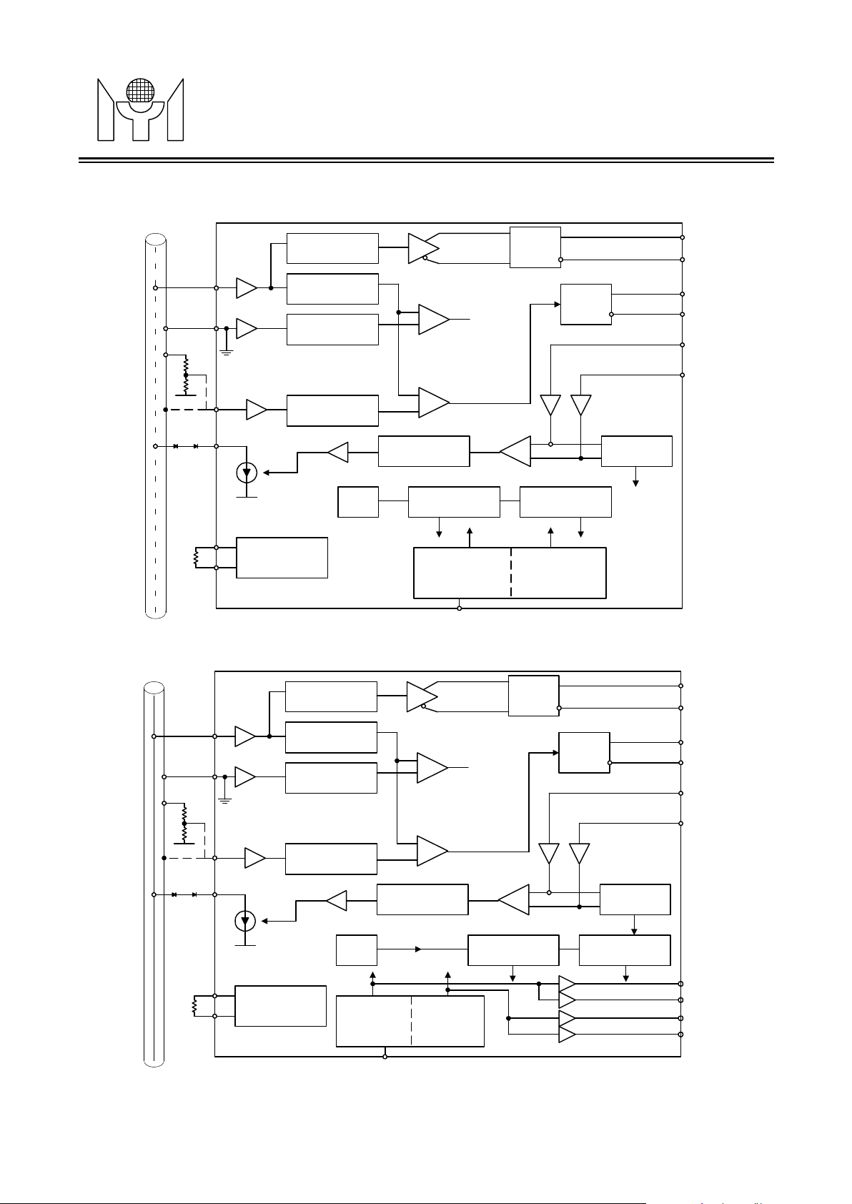
COAX
125
10K
VEE
RECV
1K
TECHNOLOGY
HIGH PASS
EQUALIZATION
1X
LOW PASS
FILTER
LOW PASS
FILTER
LOW PASS
FILTER
10MHz
OSC
TRANSMIT
STATE
MACHINE
HBE
Block Diagram for MTDX94
FXI
GND
XMT
TXO
RR+
RR-
CDS
16X
REFERENCE
MODE
CIRCUIT
COM
-
+
-
+
WAVEFORM
SHAPING
CLK/1024
CLK
TEST
RECEIVE
MACHINE
TESTMOD
STATE
CARRIER
SENSE
COLLISION
WATCH DOG
TIMER 26ms
AUI
DRIVER
+
-
AUI
DRIVER
SQUELCH
JABBER RESET
TIMER 0.4sec
LED DRIVER
FAMILY
RX+
RX-
CD+
CD-
TX+
TX-
DC/AC
XMTSQ
JAB
XMT
COL
RCV
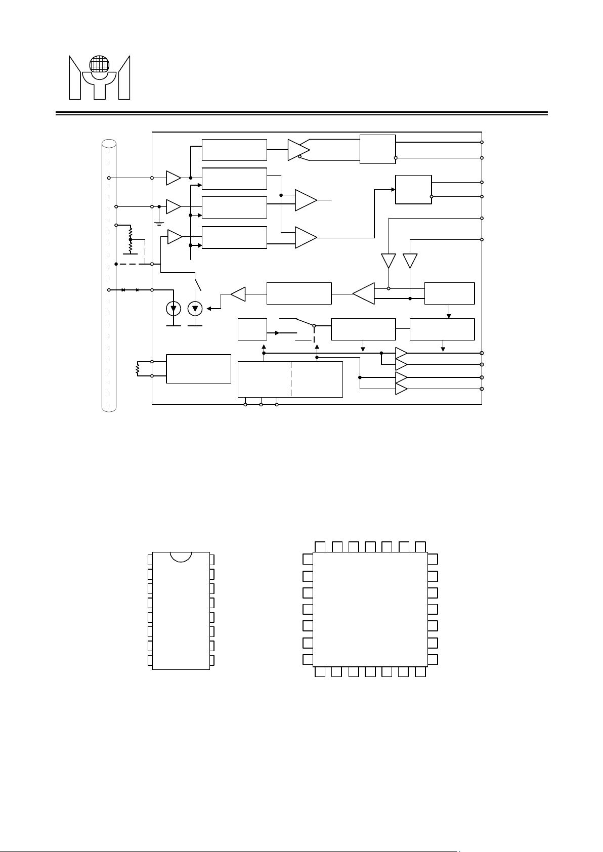
1.0 CONNECTION DIAGRAM
(1) MTDX92 Pin Diagram
CD+
CD-
RX+
VEE
VEE
RX-
TX+
TX-
1
2
3
4
MTD392N
16 PIN PDIP
5
6
7
8
16
15
14
13
12
11
10
9
CDS
TX0
RXI
VEE
RR-
RR+
GND
HBE
VEE
VEE
VEE
VEE
VEE(NC)
VEE(NC)
VEE(NC)
RX+
CD-
CD+
MTD392V
28 PIN PLCC
CDS
TXDNCRXI
VEE(NC)
VEE
VEE
VEE
VEE
VEE(NC)
RR-
3/10
MTD392 Revision 2.01 02/25/1997
Page 4

MYSON
XMT
RCV
HBE
MOD
GND
MTD392
TECHNOLOGY
(2) MTDX93 Pin Diagram
CD+
CD-
RX+
GND
VEE
RX-
COL
JAB
TX+
TX-
XMT
RCV
(3) MTDX94 Pin Diagram
CD+
1
CD-
2
RX+
3
GND
4
VEE
5
RX-
6
COL
7
JAB
8
TX+
9
TX-
10
XMT
11
RCV
12
1
2
3
4
5
6
MTD393N
24 PIN PDIP
7
(300 MIL)
8
9
10
11
12
MTD394N
24 PIN PDIP
(300 MIL)
FAMILY
24
CDS
23
TX0
22
RXI
21
VEE
20
VEE
19
RR-
18
RR+
17
GND
16
GND
15
NC
14
NC
13
HBE
24
CDS
23
TX0
22
RXI
21
VEE
20
VEE
19
RR-
18
RR+
17
GND
16
GND
15
MOD~
14
TST~
13
HBE
GND
VEE
RX-
COL
JAB
RX+
GND
VEE
RX-
COL
JAB
TX+
RX+
CD-
MTD393V
20 PIN PLCC
TX-
TX+
GND
GND
MTD394V
28 PIN PLCC
TX-
CD+
XMT
CD-
CDS
RCV
CD+
TXO
HBE
GND
TST
RXI
VEE
RR-
RR+
GND
CDS
TXD
RXI
VEE
VEE
VEE
RR-
RR+
GND
2.0 PIN DESCRIPTIONS
MTD
Name I/O
X92
PIN#
TX+,TX- I 7
HBE I 9 13 13
RR+,RR- I 11
12
MTD
X93
PIN#
9
8
10
18
19
MTD
X94
PIN#
9
10
18
19
Description
Transmission Data Input. A balanced differential line
receiver that receives input from the off-chip Manchester
Code Converter (MCC) to the Transmitter. The common
mode voltage on TX± is set internally.
Heartbeat Enabler. The CD heartbeat test is enabled when
HBE is connected to Ground and disabled when HBE is
connected to VEE.
External Resistor. A 1kW,/1% resistor should be connected
across these pins to correctly set internal operating currents.
RR+ is internally shorted to GND.
MTD392 Revision 2.01 02/25/1997
4/10
Page 5

MYSON
shield, providing a reference for the collision detection voltage
Receiving Data Output. A balanced differential output drives
this output pair from the collision detection circuitry. A 10MHz
common mode on the pull-down resistors to be pulled to VEE.
cable via one serial isolation diode for
Thinnet (10
Test Enabler.
function is disabled and all state timing is accelerated by 1024
MTD392
TECHNOLOGY
RXI I 14 22 22
CDS I 16 24 24
RX+,RX- O 3
6
CD+,CD- O 1
2
3
6
1
2
Network Receiving Input. Should be connected to the
COAX center conductor. Signals meeting receiver squelch
limits are recovered and output on RX±/RXI also detects the
collision voltage level.
Collision Detecting Sense. Connects directly to the COAX
level for receiving-mode detection. An external bias network
can be used to shift the detection threshold for transmissiondetection mode. For hybrid mode collision detection, a 400W
resistor should be connected from CDS to GND.
3
6
data recovered from the network to the MCC. These outputs
are also open sources, and pull-down resistors from 510W to
VEE are required. To minimize power dissipation, both open
source outputs are disabled during idle conditions, allowing
the common mode on the pull-down resistor to be pulled to
VEE.
1
Collision Output. A balanced differential line driver drives
2
signal from the internal oscillator is transferred to these
outputs in the event of collision or excessive transmission
(jabber), or during heartbeat condition. These outputs are
open sources, and pull-down resistors from 510W to VEE are
required. To minimize power dissipation, both open source
outputs are disabled during idle condition, allowing the
FAMILY
TXO O 15 23 23
GND 10 4
16
17
VEE 4
5
13
COL,
JAB,
XMT,
RCV,
TST- I 14
MOD- I 15
O 7
5
20
21
16
17
20
21
8
11
12
Transmitter Output. Should be connected to the coaxial
Cheapernet/
Base2) or 2 serial isolation diodes for Thicknet (10 Base5).
4
Positive Supply Pin (Ground). Should be connected to the
COAX shield.
5
Negative Power Supply. -9 volts. A 0.1mF decoupling
capacitor must be connected across GND and VEE as close
to the device as possible.
Transceiver Status Indicators. LED displays for collision,
jabber, transmission and reception. These pins are opendrain output buffers that are used to drive LED status
indicators. They are designed to supply 8 mA sinking
capability.
When both TST- and MOD- pins are shorted to
VEE, MTDX94 enters into test mode. In this mode, the jabber
times. This pin has a 50kW internal pull-up resistor.
Mode Selection. Along with the TST- pin, determines the
collision detection method of MTDX94. If both MOD- and
TST- are connected to GND, MTDX94 implements receivingmode collision detection. The typical detection threshold in
receiving-mode is -1.53V. To implement transmission-mode
collision detection, the detection threshold can be lowered by
placing a resistor bias network on the CDS pin. When the
TST- pin is connected to GND and the MOD- pin is connected
to VEE, MTDX94 uses hybrid-mode for collision detection. In
this mode, the threshold is set at -0.42V during idle or
MTD392 Revision 2.01 02/25/1997
5/10
Page 6

MYSON
should be connected between the CDS pin and GND. This pin
DC Common Mode Output Voltage (RX
) (Note2)
MTD392
TECHNOLOGY
receiving operation. During transmission, the detection
threshold is increased to -0.42V plus its own transmission
level on the CDS pin. When TST- is connected to VEE and
MOD- is connected to GND, MTDX94 uses the transmithybrid mode for collision detection. This mode is identical to
hybrid-mode, except that during idle or receiving operation,
the detection threshold is set at -1.53V. For proper operation
of hybrid and transmission-hybrid mode, a 400 W resistor
has a 50 kW internal pull-up resistor.
3.0 ABSOLUTE MAXIMUM RATINGS
DC Supply Voltage (VEE) -12V
Input Voltage GND+0.3 to VEE-0.3V
Storage Temperature -65o to 150oC
Ambient Operating Temperature 0o to 70oC
ESD Protection except RXI 2000V
FAMILY
4.0 OPERATING CONDITIONS
DC Supply Voltage (VEE) 8.55-9.45V
Operating Temperature 0o to 70oC
5.0 ELECTRICAL CHARACTERISTICS (under operating conditions) (Note 1)
Parameter Symbol Min Typ Max Unit
Recommended Supply Voltage VEE -8.55 -9.0 -9.45 V
Non-transmitting Supply Current (VEE to GND) IEE - -25 -35 mA
Transmission - -70 -80 mA
Receiving Input Bias Current (RXI) Irxi -2 - +25
Transmitting Output DC Current (TXO) Itdc 37 41 45 mA
Transmitting Output AC Current (TXO) Itac
Collision Threshold (Receiving Mode) Vcd -1.45 -1.53 -1.62 V
Collision Threshold (Hybrid Mode) (MTDX94 only)
Carrier Sense Threshold (RXI) Vcs -0.38 -0.45 -0.52 V
Differential Output Voltage (RX±,CD±)
±,CD±
Idle State Differential Offset Voltage(RX±,CD±)
Transmission Squelch Threshold(TX±) (Note 3)
Input Capacitance (RXI) Cx - 1.5 - pF
Shunt Resistance-Non-transmitting Rrxi 100 - Shunt Resistance-Transmitting Rtxo 10 - -
Vhcd -0.38 -0.45 -0.52 V
Vod
Voc -1.0 -2.0 -3.0 V
Vob - 0
Vts -175 -225 -300 mV
±28
±500
- Itdc mA
-
±1500
±40
mA
mV
mV
kW
kW
Notes:1. Testing is done under the testing load defined in Figure 6.
2. During idle condition, Voc is pulled down to VEE to minimize the power dissipation across the load
resistors connected to RX± and CD±pins.
3. For a minimum pulse width of ³40 ns.
MTD392 Revision 2.01 02/25/1997
6/10
Page 7

MYSON
MTD392
TECHNOLOGY
FAMILY
6.0 SWITCHING CHARACTERISTICS (under operating conditions) (Note 1)
Parameter Symbol Min Typ Max Unit
Receiving Start-up Delay (RXI to RX±)
Receiving Propagation Delay (RXI to RX±)
Differential Output Rise Time (RX±,CD±)
Differential Output Fall Time (RX±,CD±)
Reception and Cable Total Jitter Trj Transmission Start-up Delay Ttst - 1 2 bits
Transmission Propagation Delay Ttd - 25 50 ns
Transmission Rise Time (10%-90%) (TXO) Ttr 20 25 30 ns
Transmission Fall Time (10%-90%) (TXO) Ttf 20 25 30 ns
Ttr and Trf Mismatch Ttm Transmission Skew(TXO) Tts Transmission Turn-on Pulse Width at Vts(TX+) (Note 4) Tton 10 20 40 ns
Transmission Turn-off Delay Ttoff 130 200 300 ns
Collision Turn-on Delay Tcon - 7 13 bits
Collision Turn-off Delay Tcoff - - 20 bits
Collision Frequency (CD±)
Collision Pulse Width (CD±)
CD Heartbeat Delay (TX± to CD±)
CD Heartbeat Duration(CD±)
Jabber Activation Delay(TX± to CD±)
Jabber Reset Timeout (TX±to TXO and CD±)
Tron - 2.5 5 bits
Trd - 25 50 ns
Trr - 4 7 ns
Trf - 4 7 ns
±2
±0.5 ±3.0
±0.5 ±2
- ns
ns
ns
Fcp 8.5 10 12.5 MHz
Tcp 40 50 60 ns
Thon 0.6 1.1 1.6
Thw 0.5 1.0 1.5
ms
ms
Tja 20 26 32 ms
Tjr 300 420 550 ms
Notes: 4. For a minimum pulse amplitude of ³ -300 mV.
7.0 TIMING DIAGRAM FOR MTD392 FAMILY
INPUT
TO RXI
RX+
RX-
TX+
TX-
TXO
OUTPUT
TX+
TX-
CD+
CD-
T
ron
Figure 1. Reception Timing
50%
V
ts
T
ton
T
tst
50%
T
90%
td
10%
T
T
tf
Figure 2. Transmission Timing
T
hon
50%
50%
tr
T
T
rd
90%
10%
T
T
rf
rr
T
tidl
T
toff
T
hw
roff
Figure 3. Heartbeat Timing
7/10
MTD392 Revision 2.01 02/25/1997
Page 8

MYSON
MTD392
INPUT
to RXI
CD+
CD-
TX+
TX-
TXO
CD+
CD-
TXO
Transmitter
Output
TECHNOLOGY
0V
-1.75V
Vcd (max)
T
con
1/F
cp
Figure 4. Collision Timing
T
ja
Figure 5. Jabber Timing
25
W
Vcd (min)
T
cp
-6.8V
T
T
jr
Receiver (RX )
Collision(CD )
Outputs
+
-
coff
510
FAMILY
-1.2V
W
39
50mH*
W
39
W
510
W
Figure 6. Test Loads
VEE
8/10
MTD392 Revision 2.01 02/25/1997
Page 9

MYSON
MTD392
TECHNOLOGY
8.0 PACKAGE DIMENSION FOR 392 FAMILY
A. 24-PIN PDIP
UNIT: MIL
930+/-10
115Min
15Max
100Typ
1245+/-10
18+/-2Typ 60+/-5Typ
7Typ
15Min.
R40
35+/-5
312+/-12
R10Max
(4X)
55+/-20
65+/-4
65+/-4
FAMILY
80+/-20
10
350+/-20
250+/-4
B. 16-PIN PDIP
UNIT: MIL
15Max
130 +/-15
75+/-20
90+/-20
100+/-20
15Max
18+/-5Typ 60+/-15
760+/-20
7Ty
R40
312+/-12 100+/-20
55+/-20
60+/-4
p
35+/-5
15Min.
10
60+/-4
310Max
355+/-50
245+/-20
9/10
MTD392 Revision 2.01 02/25/1997
Page 10

MYSON
MTD392
C. 28-PIN PLCC
UNIT: INCH
TECHNOLOGY
0.045*45
0
0.453 +/-0.003
0.4902 +/-0.005
PIN #1 HOLE
0.453 +/-0.003
0.050 TYP.
0.026~0.032 TYP.
0.490 +/-0.005
0.180 MAX.
0.013~0.021 TYP.
70TYP.
0.070 0.070
FAMILY
0.020 MIN.
0.410 +/-0.02
0.300
0.010
D. 20-PIN PLCC
UNIT: INCH
0.045*45
0.050 TYP.
0.353 +/-0.003
0.390 +/-0.005
0
PIN #1 HOLE
0.353 +/-0.003
0.390 +/-0.005
0.180 MAX.
0.013~0.021 TYP.
70TYP.
0.070 0.070
0.020 MIN.
0.010
0.200
0.310 +/-0.02
10/10
MTD392 Revision 2.01 02/25/1997
 Loading...