

Page 1
ISO-CMOS ST-BUS FAMILY
MT8982
Small Digital Switch (MiniDX)
Features
• ST-BUS/G CI c om pa tib le swit ch ma tr ix
• 64 channel non-bl ocking tim e swit ch
• 2 x 32 channe l serial input s and o utpu ts
• Per-channel t ristate contro l
• 4-pin serial microprocessor i nterface
• Patented me ssag e m ode
• Low power co nsu mptio n (10 m W)
• Single 5 volt sup ply
Applications
• Cost sensi tive d igital switch ing ap plica tion s
• Digital key telephone systems
• GCI/ST-BUS conversion
• ST-BUS device control interface
• ISDN telephon e set su pport c ircuit
• Interproce ssor co mmuni cati on
ISSUE 6 May 1995
Ordering Information
MT8982AC 16 Pin Cerami c DIP
MT8982AE 16 Pin Plas tic D IP
MT8982A S 16 Pin SO IC
MT8982A N 20 Pin SSOP
-40 to +85°C
Descript io n
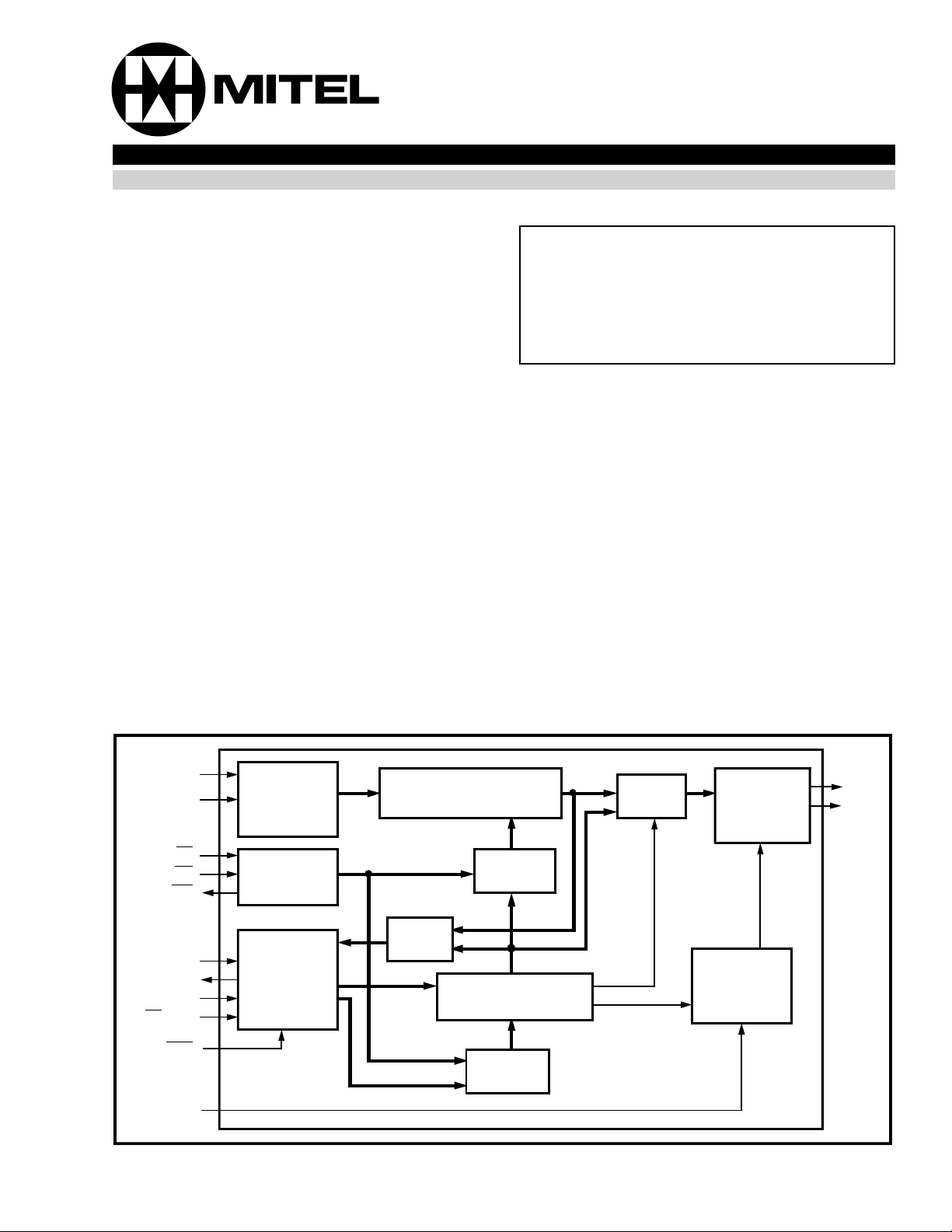
The MT8982 Small Digital Switch (MiniDX) is a nonblocking CMOS time switch with a capacity of up to
64 - 8 bit Time Division Multiplexed (TDM) encoded
voice or data channels. It is a size-optimized version
of MITEL's successful MT8980D Digital Switches,
providing switching capability in cost sensitive
applications such as telephone sets and digital key
systems. The TDM interface to the device is via two
pairs of 2048 kbit/s serial streams with 32 64 kbit/s
channels per stream (ST-BUS). A serial microport
provides access to the device for programming the
required connections. The serial microport is
compatible with most common microcontrollers. The
unique message mode capability allows the MT8982
to act as a controller for other members of MITEL's
ST-BUS family of components.
STi0
STi1
F0i
C4i
F0o
RxD/CSTi0
TxD/NC
SCLK/CSTi1
/CMS
CS
MPS
ODE
Serial
to
Parallel
Converter
Address
Counters
Serial
Microport
64 x 8
Data Memory
Address
Mux
Data
Mux
64 x 9
Connect Memory
Address
Mux
Figure 1 - Functional Block Diagram
Output
Mux
Parallel
Serial
Converter
3-State
Control
to
STo0
STo1
2-31
Page 2
MT8982 ISO-CMOS
STi0
STi1
STo0
STo1
RxD/CSTi0
TxD/NC
SCLK/CSTi1
VSS
16 PIN CERDIP/PLASTIC/SOIC
Pin Description
Pin #
Name Description
16 20
1-2 1-2 STi0-
STi1
3-4 4-5 STo0-
STo1
5 6 RxD/
CSTi0
20
19
18
17
16
15
14
13
12
11
VDD
ODE
IC
MPS
F0o
NC
F0i
NC
C4i
CS
NC
NC
1
2
3
4
5
6
7
8
9
10
20 PIN SSOP
1
2
3
4
5
6
7
8
16
15
14
13
12
11
10
VDD
ODE
IC
MPS
F0o
F0i
C4i
9
CS
STi0
STi1
STo0
STo1
RxD/CSTi0
TxD/NC
SCLK/CSTi1
VSS
Figure 2 - Pin Connections
Serial TDM Inp ut 0 and 1 (Inputs). 2048 kbit/s input data streams con taining 32 8-bit
channels synchronized to F0i
.
Serial TDM Output 0 and 1 (Outputs). 2048 kbit/s output data strea ms conta ining 32
8-bit channels synchronized to F0i
Received Data/Control Stream Input 0 (Input). When MPS
microport data clocked in by the rising edge SCLK. When MPS
.
is low, this pin receives serial
is high, this pin receives a
2048 kbit/s serial TDM stream containing 32 8-bit channels, wh ich are writt en i nto the
Connect Memory locations co rresponding to STo0.
6 7 TxD Transmit Data (Output). When MPS
by the falling edge of SCLK. When MPS
7 9 SCLK/
CSTi1
Serial Micr op ort Clo ck/ Con trol Stream Inp ut 1 (Inpu t ). When MPS
receives a clock which is used to clock data to/from a microcontroller via a serial microport.
When MPS
is high, this pin receives a 2048 kbit/s serial TDM stream containing 32 8-bit
is low, serial microport data is clocked out on this pin
is high this output is disabled.
is low, this pin
channels, which are written into the Conn ect Me mory locat ions correspo nding to STo1.
810 V
911 CS
10 12 C4i
Power Inpu t. Negative supply (ground).
SS
Chip Select (Input). When MPS is low, a low on this pin enables the serial microport. A
high on this pin disables RxD and tristates TxD. When MPS
is high, this pin must be low.
Serial TDM Cl ock (In pu t). This clock input is used to clock the TDM data into and out of
the device and refreshes the internal dynamic RAM. The clock rate is 4.096 MHz and data
three-quarters of the way through a bit period.
11 14 F0i
is clocked in on the rising edge of C4i
Frame Puls e (Inp ut). This input is the frame synchronization pulse for the 2048 kbit/s
serial TDM streams. It may be either active low stradling the frame bounda ry (ST-BUS) or
active high at the beginning of timeslot 5 (GCI).
12 16 F 0o
Frame Puls e (Outpu t). This pin outputs a fram e pulse in the opposite format to F0i (GCI
or ST-BUS) delayed or advanced by five channels.
13 17 MPS
Microport Select (Input). When this pin is held low, the serial microport is in normal mode.
When this pin is high, the microport is in se rial bus mode .
14 18 IC Internal Connectio n. Tie to V
for normal ope ration.
SS
15 19 ODE Output Drive Enable (Input). When this pin is held high, the STo0 and STo1 output drivers
function normall y. When this pin is low, STo0 and STo1 are tristated.
NB: When ODE is high, individual channels on STo 0 and STo1 can be tristated under
software control.
16 20 V
3,8,
13,15
2-32
Power Inpu t. Positive supply.
DD
NC No Connection.
Page 3

ISO-CMOS MT8982
Functional Description
The MT8982 (MiniDX) provides cost effective time
switching capability for small size applications
utilizing up to two serial Time Division Multiplexed
(TDM) streams. Each TDM stream consists of 32 64
kb/s channels, giving the MiniDX a maximum
capacity of 64 channels. The input framing signal
may be either a ST-BUS or a GCI frame pulse. The
MT8982 will output a delayed or advanced frame
pulse in the opposite format to permit conversion
between the two forma ts.
The MiniDX can switch data from any channel in one
of the two serial input TDM streams to any channel in
either of the two serial output TDM streams. The
microcontroller controlling the MiniDX writes to the
MT8982 Connect Memory to establish the
connection between the required input TDM channel
and the selected output TDM channel(s). By reading
the Connect Memory the microcontroller can check
switched connections which have already been
established.
The MiniDX can also operate in message mode
where the microcontroller transmits the data on the
TDM serial stream. The microcontroller writes to the
MT8982 Connect Memory to transmit data on the
required output TDM channels. Reading the Data
Memory of the MT8982 allows the microcontroller to
receive messages from TDM input channels. These
operations are useful for control of other ST-BUS
components or for interprocessor communication.
formatted frame pulse is active high at the beginning
of timeslot 5 (relative to the MT8982) and idles low.
The MT8982 automatically determines the type of
frame pulse from the level of the idle over five clock
periods. A ST-BUS formatted fr ame pulse r e sets the
internal addr ess counters to zero . A GCI formatted
frame pul se resets the counters to five.
F0o
outputs a frame pulse in the opposite format. If
is a ST-BUS formatted fra m e pul se, F0o will be a
F0i
GCI formatted frame pulse delayed by five channels
after F0i. If F0i
will be a ST-BUS formatted frame pulse delayed by
27 chann el s (32 - 5).
During normal operation every second falling edge of
the clock marks a timeslot boundary and the input
data is clocked in by the rising edge, three-quarters
of the way into the b it cell. The ma ster clo ck must
be 4.096 MHz for the F0o
receive a GCI formatted F0i
Data which is output onto a TDM serial output
channel may come from two sources; the Data
Memory or the Connect Memory. If a channel is
configured in connection mode, the source of output
data is t he Data Mem ory. If a chann el is co nfigure d
in message mode, the source of the output data is
the Conne ct Memory. Data destined fo r a particular
channel on the serial output links is read from the
data or connect memory in the previous channel
timeslot. This allows for delay in RAM access and
parallel-to-serial conversion. Each output data
channel can also be placed in tristate mode.
is a GCI formatted frame pulse, F0o
signal to be valid and to
.
Hardware Description
TDM Interfa c e
The MT8982 continuously receives TDM serial data
at 2048 kbit/s through two serial inputs. These serial
streams are then converted into a parallel format and
stored sequentially in a 64x8 bit Data Memory. The
sequential addressing is generated by an internal
counter that is reset by the input 8 kHz frame pulse
(F0i
) which marks the frame boundaries of the
incoming serial data stream. This counter increments
with each timeslot so that it matches the binary count
of the timeslot of the incoming data. The TDM
timeslot count always corresponds to the ST-BUS
channel positions. An extra address bit is used to
differentiate between the two input data streams.
The input 8 kHz frame pulse may be either ST-BUS
or GCI formatted. A ST-BUS formatted frame pulse
is an active low signal which straddles the frame
boundary. It idles high the rest of the time. A GCI
When an output channel is in connection mode, the
TDM output data is read from a Data Memory
location pointed to by an address stored in the 64x8
bit Connect Memory. The Connect Memory locations
are addressed sequentially, with each location
corresponding to an output TDM link/channel. In the
channel time before the data is to be output, the
contents of each Connect Memory location are
output to the address bus of the Data Memory. The
contents of the Data Memory at the selected address
are then transferred to the parallel-to-serial
converter. The parallel-to-serial converter outputs
onto the TDM serial stream during the correct
channel time. By having the output channel specify
the input channel, the user can route the same input
channel to several output channels. This function is
useful for broadcasting or resource channel uses.
2-33
Page 4
MT8982 ISO-CMOS
When an output channel is in message mode, the
data for the output channel originates from the
microcontroller. The microcontroller writes data to
the Connect Memory location which corresponds to
the output link and channel number. The contents of
the Connect Memory are transferred directly to the
serial-to-parallel converter one channel time before it
is to be output. The Connect Memory data is output
MSB first, repetitively once per frame, until it is
changed by the microcontroller.
If the output channel is configured in tristate mode,
the TDM serial stream output will be placed in high
impedance during that channel time. This mode is
entered by configuring the channel into connection
mode and then setting the tristate control bit. All
channels on both output TDM streams can be
tristated by pulling pin 16 (ODE) low. T his overrides
the individual channel programming.
The Data and Connect Memories are dynamic
memories. They are refreshed by the sequential
addressing generated by C4i
.
Microcontroller Interface
The MT8982 is controlled via a synchronous, serial
microport. The microport is compatible with Intel's
MCS-51 serial port Mode 0 specifications, Motorola's
Serial Peripheral Interface (SPI) specifications, and
National's MicroWire specifications. The port
consists of a transmit data line (TxD), a receive data
line (RxD), a chip select line (CS
), and a
synchronous clock input (SCLK). All memory
locations and control functions on the MiniDX are
accessed through this port. The microport may also
be configured in serial bus mode where data is
clocked into the Connect Memory in the same way
as STi0 and STi1 are clocked into Data Memory.
In serial microport mode, CS must be low to enable a
microport access. SCLK clocks the serial microport
data in or out through RxD and TxD, LSB first. The
TxD output driver is tristated when it is inactive. This
allows RxD and TxD to be connected together for a
single TxD/RxD line as u sed in the INTEL MCS-51
microcontrollers. Figure 3 shows a serial microport
access cycle.
RxD
TxD
SCLK
CS
COMMAND/ADDRESS DATA INPUT/OUTPU T
D0D1D2D3D4D5D6D
➁
➂
➀
D0D1D2D3D4D5D6D
7
D0D1D2D3D4D5D6D
A microport access cycle (microcycle) begins with a
falling edge on CS
. Eight bits of data are clocked
into RxD by the rising edge of SCLK. Two of these
eight bits indicate whether the microcycle operation
is a read or a write, the rest of the bits are used for
addressing. These eight bits are defined as the
command/ address byte (Table 1). If the microcyle
operation is a write, another eight bits are clocked
➃
➀
7
7
➃
COMMAND/ADDRESS
D0D1D2D3D4D5D6D
D0D1D2D3D4D5D6D
7
7
➀ Minimum delay between accesses equals 3.0 µsec.
➁ The Mini Dx: - latches received data in on the rising edge of SCLK
➂ The falling edge of CS
➃ Subsequent write microcycles may flow without raising CS
- outputs transmit data on the falling edge of SCLK
indicates that a COMMAND/ADDRESS byte will be transmitted. Subsequent byte is always data.
Figure 3 - Serial Microport Timing
2-34
. CS must go high after a read microcycle.
Page 5

ISO-CMOS MT8982
into RxD by the rising edges of the next eight SCLK
cycles. If the operation is a read, eight data bits are
clocked from TxD by the falling edges of the next
eight SCLK cycles. The rising edge of CS
TxD after th e las t tr a ns mitted bit.
Successive write microcycles can take place while
CS
remains low, with each microcycle following the
sequence of a command/address byte followed by a
data byte. CS
Note that a command/address byte must always
follow the h i gh t o l ow tr a n si ti o n on CS
When the MPS
is pulled low, the microport is put into serial bus
mode. Pins RxD and SCLK become CSTi0 and
CSTi1, respectively, and are configured as 2048 kbit/
s serial streams with 32 channels each. The frame
and timeslot boundaries are determined by F0i and
C4
. Each channel on CSTi0 and CSTi1 is stored in
the connect memory address corresponding to the
link and channel number. The Data Memory and the
Connect Memory cannot be read when the microport
is in serial bus mode.
must go high after a read microcycle.
input is pulled high and the CS input
tristates
.
Device Timin g
During each TDM timeslot, eight read or write
operations occur internally in the MT8982. These are
shown in Figure 4. During the first two bit periods,
data received in the previous timeslot on the two
input TDM streams is loaded into the Data Memory.
Bit periods 2 and 6 are serial microport access
windows; data may be read from, or written to any
accessible memory location. During bit periods 3
and 5, data is read from the connect memory for the
next timeslot on links 0 and 1 respectively. The Data
Memory locations which are addressed by the
previous reads of the connect memory are accessed
during bit periods 4 and 7.
When the microport is in serial bus mode, bit periods
2 and 6 have a slightly different function. Data from
the previous timeslot of CSTi0 and CSTi1
respectively is written to the corresponding connect
memory locations.
The transfer of information from the input TDM
streams to the output TDM streams results in a delay
through the MT8982. This delay is dependent only
on the combination of source and destination
Bit Name Description
7 Stream Stream. This is the most significant bit of the address for the memory location that
is to be accessed. It corresponds to one of the TDM serial streams (0-1).
2-6 Ch0-Ch4 Chan nel 0-4. These bits are the five least signif icant bit s of the address for the
memory location that is to be accessed. The binary value of these bits correspond
to a TDM channel (0-31).
0-1 Cmd0-Cmd1 Command Select 0-1. These two bits define the four command operations for the
MT8982. The destination addressed by the co mmand is def ined in bits 2-7 of the
Command/Address byte.
Cmd0-Cmd1
0-0 Read from Connect Memory.
0-1 Write to Connect Memory and set connection mode.
1-0 Read Data Memory.
1-1 Write to Connect Memory and set message mode.
Table 1. Co mmand Addres s Byte
Bit Name Description
7 NA Unused.
6ODEOutput Drive En abl e. When this bit is set, the addressed TDM channel is placed
in tristate. When low, the output is enabled.
5STiInput Stream. This bit defines the input TDM stream from which the output data is
sourced (0-1).
0-4 SC0-SC4 Source Channel 0-4. The binary value of these bits defines the input channel from
which the output data is sourced (0-31).
Table 2. Connect Memory Connection Mode Data Byte
2-35
Page 6

MT8982 ISO-CMOS
Channel 31 Channel 0
F0i
C4
Microport
Mode
Serial Port Mode
Bit 0 Bit 7Bit 6Bit 5Bit 4Bit 3Bit 2Bit 1
Wr DM
Link 0
Ch 31
Wr DM
Link 1
Ch 31
µP µP
Wr CM
Link 0
Ch 31
Figure 4 - Int erna l Me mory Ac cess Wind ows
channels and is not dependent on the input and
output streams. The delays are given in Table 3.
The maximum delay is one frame plus one channel;
the minimum delay is two channels.
Input
Channel
Output
Channel
Delay
n m = n, n+1 m- n + 32 channels
n m > n+1 m- n channels
n m < n 32- (n-m) channels
Table 3. Input Channel to Output Channel Delay
Times
The following delays apply to writing data to the
Connect Memory in message mode. For stream 0,
data must be written to a Connect Memory location
at least one timeslot before the corresponding output
channel or the output data will be delayed by one
frame. For stream 1, data must be written at least
two timeslots before the output channel or the output
data will be delayed by one frame.
Rd CM
Link 0
Ch 1
Rd DM
Link 0
Ch 1
Rd CM
Link 1
Ch 1
Wr CM
Link 1
Ch 31
Rd DM
Link 1
Ch 1
Device Programming
Microport Mod e
In serial microport mode, the MT8982 is
programmed and read using microcycles which
consist of a command/address byte followed by a
data byte.
The Command/Address Byte is shown in Table 1.
Bits 0 and 1 are the command bits (Cmd0-1), and
are used to indicate the type of microcycle access.
The microcontroller can read the Data Memory, read
or write the Connect Memory, and set per-channel
message or connection mode. Bits 2 to 6 of the
command/address byte (Ch0-Ch4) correlate to a
channel on a TDM stream (0-31). Bit 7 (STREAM)
correlates to stream 0 or stream 1. These bits
address the corresponding Data Memory or Connect
Memory location.
The microcycle operations selected by the
command/address byte are as follows:
2-36
Read Con nect Me mory (Cm d0-1 : 0,0)
Bits 0 to 7 of the addressed Connect Memory
location will be transmitted to the microcontroller
in the following data byte. Depending on what
the last Connect Memory write mode was, the
data transmitted could be a message byte or a
Connection Mode data byte.
Page 7

ISO-CMOS MT8982
Write Connect Memor y - Set Connec tion Mode
(Cmd0-1: 0,1 )
The corresponding output channel to the
addressed Connect Memory location is
configured in connection mode. The Connection
Mode Data Byte (Table 2) will be received by the
MT8982 in the following data byte. Bits 0 to 4
(SC0-SC4) select the source input channel for
switching to this output channel. Bit 5 (STi)
selects the input stream. Bit 6 (ODE) enables/
disables tristate for this channel. Bit 7 is unused
in connection mode.
Read Data Memory (Cmd0-1: 1,0)
The contents of the addressed Data Memory
location are transmitted to the microcontroller in
the following data byte.
Write Connect Memory - Set Message Mode
(Cmd0-1: 1,1 )
The corresponding output channel to the
addressed Connect Memory location is
configured in message mode. The following data
byte will be received by the MT8982 and written
to the address Connect Memory location. The
data byte will be output directly to the
corresponding output channel.
The following example shows a typical programming
sequence for the MT8982. A connection is to be
made from stream 1 channel 6 to stream 0 channel
15:
• The microco ntrol ler pulls CS
• The microc ont roller transmi ts eight cloc k pu lses
to SCLK and a Command/Address byte, HEX
3E, to RxD. The Command/Address byte
addresses output channel 15, stream 0,
configures that channel as connection mode
and identifies the microcycle as a write to the
Connect Memory.
• The microcontroller transmits another eight
clock pulses to SCLK and sends the
Connection Mode Data Byte, HEX 26, to RxD.
The Connection Mode Data Byte addresses
input chan nel 6, stream 1 in the Data Memory.
Note that a t lea st two m icr osec onds m us t occu r
between t he two acce sses.
low.
The connection is now complete. The
microcontroller may now check that the connection is
correct:
• The microcontroller transmits eight clock pulses
to SCLK and a Command/Address byte, HEX
3C, to RxD. The Command/Address byte
addresses output channel 15, stream 0 and
identifies the microcycle as a read from the
Connect Memory.
• The microcontroller transmits another eight
clock pulses to SCLK. The MT8982 outputs the
Connect Memory data, HEX 26, on TxD. At
least two microseconds must occur between
the two accesses to ensu re that the Mi niDX can
clock out the data.
•CS
This connection is only in one direction. To make a
bidirectional connection the MT8982 must also be
programmed to connect stream 0 channel 15 to
stream 1 channel 6.
Serial Bus Mode
When the microport is in serial bus mode the
MT8982 is programmed via the two ST-BUS serial
streams CSTi0 and CSTi1. Each channel in these
two streams is wr it te n d ire ctly into t he correspond i n g
address in the Connect Memory. The data written to
the Connect Memory is always the Connection Mode
Data Byte as described in Table 2. To set up a
connection, the Connection Mode Data Byte is
transmitted to the MT8982 on the CSTi stream and
channel number which is the same as the desired
STo stream and channel number. As long as the
device remains in serial bus mode, the Connection
Mode Data byte must be transmitted continuously,
every frame , to mainta in the conne ct ion .
Message mode is not available when the device is in
serial bus mode. Also, neither the Connect Memory
nor the Data Memory can be read while the device is
in serial bus mode. MITEL’s MT8980, MT9080 and
MT8920 devices can all be used as programmable
parallel-to-ST-BUS serial interfaces for CSTi0 and
CSTi1.
Initialization
On power up the contents of the Connect Memory
can be in any state. In order to prevent false
programming of peripheral ST-BUS devices or false
data transmission, ODE should be kept low during
power up. This will keep the two TDM outputs in high
impedance until the MT8982 Connect Memory is
programmed.
goes high to terminate the session.
2-37
Page 8

MT8982 ISO-CMOS
Applications
Digital Key Telephone System
Figure 5 shows a block diagram of a Digital Key
Telephone System (DKTS) implemented with the
MT8982. This DKTS can support up to 64
connections organized in any combination of
subscriber lines or trunks. A very small system
consisting of six lines and one trunk can very easily
and economically be designed on one board. The
MT8982 significantly reduces the tracking and board
space required for competitive switch matrices.
Distributed S witch ing Sys tem
The MT8982 can be used to distribute switching
capability in a very large system. In Figure 6 the
MT8982 is shown with the microport in serial bus
mode. This allows the central microprocessor to set
up and tear down connections at the remote
locations by programming the remote MT8982's
through their CSTi pins. A microcontroller in each
remote switch would not be required.
Primary Rate Serial Controller
ST-BUS to GCI Conversion
The MT8982 MiniDX may be used to provide a
gateway between MITEL's ST-BUS family of
components and an architecture which utilizes the
General Circuit Interface (GCI) operating at 2048
kbit/s (Figure 8). The MT8982 performs automatic
adaptation of the different frame pulse signals. The
master frame pulse to the MT8982 can be supplied
either by the ST-BUS or the GCI components. The
MT8982 will then provide either a delayed or
advanced frame pulse to the other components as
shown in Figures 9 and 10.
When an ST-BUS component is supplying the
master frame pulse (F0i
output frame pulse (F0o
), the MiniDX will supply the
) delayed by five channels.
This ensures that frame integrity is maintained
between the ST-BUS and GCI components. When a
GCI component supplies the master frame pulse
), F0o is advance d by fiv e ch anne ls.
(F0i
Figure 8 shows a block diagram of a GCI to ST-BUS
conversion circuit. External inversion of the clock
signal is required between the ST-BUS and GCI
components because the ST-BUS and GCI master
C4 clocks use different edges to mark bit boundaries.
Figure 7 shows the MT8982 used in a primary rate
serial control application. The MT8982 is used as
the control interface from a microcontroller to
MITEL’s MH89760/790 T1 Primary Rate Interfaces
using the microcontroller’s serial microport. The
MT8982 offloads signalling and trunk control
functions fro m the central switch matrix leav ing more
capacity for switching.
CENTRAL DKTS CONTROLLER
MT8972
DNIC
MT8972
DNIC
•
•
•
MT8972
DNIC
To program a connection between a ST-BUS channel
and a GCI channel, some channel conversion is
necessary. Figure 11 shows the relationship
between the ST-BUS basic access frame and the
GCI basic access frame. Because the MT8982 shif ts
the GCI frame pulse (input or output) by five
channels, all of the GCI channels must be
incremented by five to be correctly addressed by the
MT8982
MiniDx
Microcon troll er
MH88630/1
C.O. Trunk
To
Central
Office
2-38
Figure 5 - Digital Key Telephone System (DKTS)
Page 9

MT8982
MiniDx
ISO-CMOS MT8982
µP
Large Central Switch &
Central Control
MT9080/85’s
Large Switch
Matrix
STi0
STi0
CSTi0
CSTi1
Small Remote Switch 1
•
•
•
STi0
STo0
CSTi0
CSTi1
Small Remote Switch n
MT8982
MiniDx
STi1
STo1
STi1
STo1
Figure 6 - Distr ibute d Swi tching System
Subscriber
Interface 0
•
•
Subscriber
Interface 32
•
•
•
Subscriber
Interface 0
•
•
Subscriber
Interface 32
Parallel
µP Interface
Serial
µP Interface
MT8980 Switch
Matrix
STo0
STi0
MT8952
D-Channel Protocol
Controller
CDSTo
CDSTi
MT8982
MiniDx
STo0
STo1
STi0
MH89760/790
T1 Trunk
DSTi
DSTo
CSTi0
CSTi1
CSTo
Figure 7 - Pr imar y Ra te Seri al Cont rolle r
2-39
Page 10

MT8982 ISO-CMOS
MT8982 MiniDx
STo0
STi0
C4i
F0i F0o
GCI CLK
(4.096 MHz)
GCI Frame Pulse
PCM
Streams
Figure 8 - GCI/ST-BUS Interface
MT8982. Therefore, to connect GCI channel B1 to
ST-BUS channel B1, the MT8982 must be
programmed to connect channel 5 to channel 2. The
five channel offset ensures that all four basic rate
channels will be switched together within one frame
period, regardless which direction the data is being
switched.
F0i
Channel 0 Channel 4 Channel 5
Mitel Basic Rate
Phone Com pon en ts
STi1
STo1
ST-BUS Frame Pulse
STo
STi
C4i
F0i
The five channel offset for GCI channels is required
even in GCI to GCI switching systems. For example,
to switch GCI channel B1 to GCI channel B2, the
MT8982 must be programmed to connect channel 5
to channel 6.
C4i
F0o
F0i
C4i
F0o
ST-BUS
Figure 9 - ST-BUS/GC I Timing wi th ST-BUS as Mast er
Channel 0 Channel 4 Channel 5
Figure 10 - ST-BUS/GCI Timing with GCI as Mas ter
CH0 CH1 CH2 CH3
D
C
B
1
B
2
- ST-BUS and MiniDx Channels
2-40
GCI
B
1
CH0(5) CH1(6) CH2(7) CH3(8)
B
2
M
D and C/I
- GCI (MiniDx) Channels
Figure 11 - Switching GCI and ST-BUS Basic Rate Access Channels
Page 11

Absolute Maximum Rating s *
Parameter Symbol Min Max Units
ISO-CMOS MT8982
1 P ow e r suppl y voltage V
DD-VSS
2 Voltage on any pin V
3 C u rrent at any pin (other than suppl y) I
4 S torage tempe rature T
5 Package power dissipation P
* Exceeding these values ma y cause perm anen t dama ge. Functi onal operati on und er these cond ition s is not implied.
Recommended Operating Conditions - Voltages are with respect to ground (V
Characteristics Sym Min Typ
1 Operating Temperature T
2 Power supply V
OP
DD
3 Input voltage V
‡ Typical figu res are at 25°C and are for desi gn aid only: not guarante ed and not subject to prod ucti on testin g.
-40 +85 °C
4.5 5.5 V
V
I
SS
DC Electrical Characteristics - Voltages are with respect to ground (V
Characteristics Sym Min Typ
1 Operating su pply voltag e V
2 Operating su pply current I
3 Static supply current I
4 High level input V
DD
DD
DDS
IH
5 Low level input voltage V
6 Input leakage current I
7 Low level output volta ge V
8 High level output voltage V
9 Output low (sink) current I
10 Output high (source) current I
‡ Typical figu res are at 25°C and are for desi gn aid only: not guarante ed and not subject to prod ucti on testin g.
IH/IIL
OL
OH
OL
OH
4.5 5.0 5.5 V
2.0 V
IL
2.4 V IOH = 2.0 mA
4.0 mA V
2.0 mA V
VDD-V
SS
I
O
S
D
‡
Max Units Test Conditions
V
DD
) unless otherwise stated.
SS
‡
Max Units Test Conditions
VSS-0.3 VDD+0.3 V
-65 +150 °C
) unless otherwise stated.
SS
V
2.0 mA O utp uts unloa ded
100 µA All inputs =V
0.8 V
10.0 µAVIN=V
SS
0.4 V IOL = 4.0 mA
=0.4 V
OUT
=2.4V, VDD=4.5V
OUT
6V
100 mA
1000 mW
DD
or V
DD
AC Electrical Characteristics† - Serial Microport (see Figure 12) - Voltages are with respect to ground
(V
) unless otherwise stated.
SS
Characteristics Sym Min Typ
1 Chip Select Setup Time t
2 RxD Input Setup Time t
3 RxD Inp ut Hold Time t
4 T xD Output Delay t
5 T xD Output Tristate Delay t
6 SCLK Pulse Width High t
7 SCLK Pulse Width Low t
8 Command/Data Byte Delay Time t
† Timing is over recommended temperature & power supply voltages.
‡ Typical figu res are at 25°C and are for desi gn aid only: not guarante ed and not subject to prod ucti on testin g.
* High impedance is measured by pulling to the appropriate rail with R
cs
rs
rh
td
daz
ppwh
ppwl
cdbd
5ns
40 ns
0ns
190 ns
190 ns
, with timing corrected to cancel time taken to discharge CL.
L
‡
Max Units Test Conditions
80 ns CL=50pF, RL=1kΩ
140 ns CL=50pF, RL=1kΩ*
2 µs
2-41
Page 12

MT8982 ISO-CMOS
t
cs
CS
t
ppwh
t
ppwl
SCLK
t
t
rh
rs
t
cdbd
RxD
TxD
F0i
(ST-BUS)
F0i
(GCI)
bit 0
bit 7
bit 7
t
daz
t
t
td
td
bit 0
Figure 12 - Serial Microport Timing
10 cycles of C4i
t
t
fs
fh
t
t
fs
fh
C4i
DSTo0-1
DSTi0-1
CSTi0-1
2-42
t
sdaa
t
t
sdaz
t
ss
t
sh
sdza
Figur e 13 - TD M B us Tim i ng
Page 13

ISO-CMOS MT8982
AC Electrical Characteristics† - TDM Bus (See Figures 13 and 14a, 14b). Voltages are with
respect to ground (V
) unless otherwise stated.
SS
Characteristics Sym Min Typ
‡
Max Uni ts Test Conditions
1 Frame Pulse Input Setup Time t
2 Frame Pulse Input Hold Time t
3 Serial Output Delay;
t
fs
fh
sdaa
10 ns 4 meg mode
5
5
ns
cycles
100 ns CL=50pF
Active to Active
4 Serial Output Delay;
Active to High Z
5 Serial Output Delay;
t
t
sdaz
sdza
200 ns CL=50pF
R
150 ns CL=150pF
High Z to Active
6 Serial Input Setup Time t
7 Serial Input Hold Time t
8 Frame Pulse Output Delay t
9 ODE Low to Serial Out High Z t
10 ODE High to Serial Out Active t
11 C4 Clock Pul se Width Low t
12 C4 Clock Pulse Width High t
13 C4 Clock Period t
† Timing is over recommended temperature & power supply voltages.
‡ Typical figu res are at 25°C and are for desi gn aid only: not guarante ed and not subject to prod ucti on testin g.
* High impedance is measured by pulling to the appropriate rail with R
ss
sh
fd
saz
sza
c4l
c4h
c4
20 ns
10 ns
70 ns
125 ns CL=50pF, RL=1kΩ*
50 ns CL=50pF, RL=1kΩ
25 100 209 ns tc4 = 244 ns
35 100 219 ns tc4 = 244 ns
150 244 ns
, with timing corrected to cancel time taken to discharge CL.
L
=1kΩ*
L
F0o (ST-BUS)
C4i
F0o (GCI)
t
fd
t
fd
t
c4l
t
fd
Figure 14a - TDM Bus Timing - F0o/Clock Timing
ODE
STo0-1
t
saz
t
sza
t
c4
t
c4h
t
fd
Figure 14b - ODE Timing
2-43
Page 14

MT8982 ISO-CMOS
NOTE S:
2-44
 Loading...