

Page 1
ISO-CMOS ST-BUS FAMILY
MT8981D
Digital Switch
Features
• Mitel ST-BUS compatible
• 4-line x 32-channel inputs
• 4-line x 32-channel outputs
• 128 ports non-blocking switch
• Single power supply (+5 V)
• Low power consumption: 30 mW Typ.
• Microprocessor-control interface
• Three-state serial outputs
ISSUE8 March 1997
Ordering Information
MT8981DE 40 Pin Plastic DIP
MT8981DP 44 PLCC
-40°C to +85°C
Description
This VLSI ISO-CMOS device is designed for
switching PCM-encoded voice or data, under
microprocessor control, in a modern digital
exchange, PBX or Central Office. It provides
simultaneous connections for up to 128 64 kbit/s
channels. Each of the four serial inputs and outputs
consist of 32 64 kbit/s channels multiplexed to form a
2048 kbit/s ST-BUS stream. In addition, the MT8981
provides microprocessor read and write access to
individual ST-BUS channels.
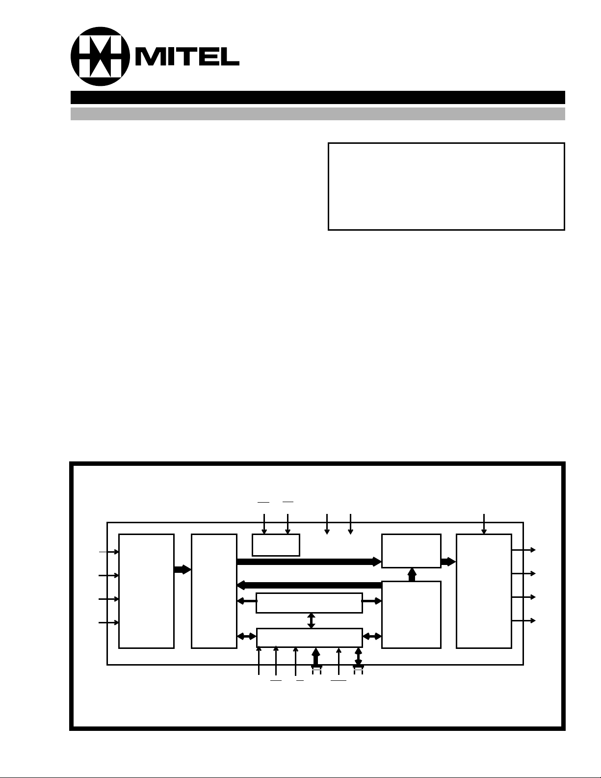
STi0
STi1
STi2
STi3
Serial
to
Parallel
Converter
V
DD
Data
Memory
F0i
C4i
Frame
Counter
Control Register
Control Interface
DS
CS R/W A5/A0DTA D7/
Figure 1 - Functional Block Diagram
V
SS
Output
MUX
Connection
Memory
D0
ODE
Parallel
to
Serial
Converter
STo0
STo1
STo2
STo3
2-17
Page 2
MT8981D ISO-CMOS
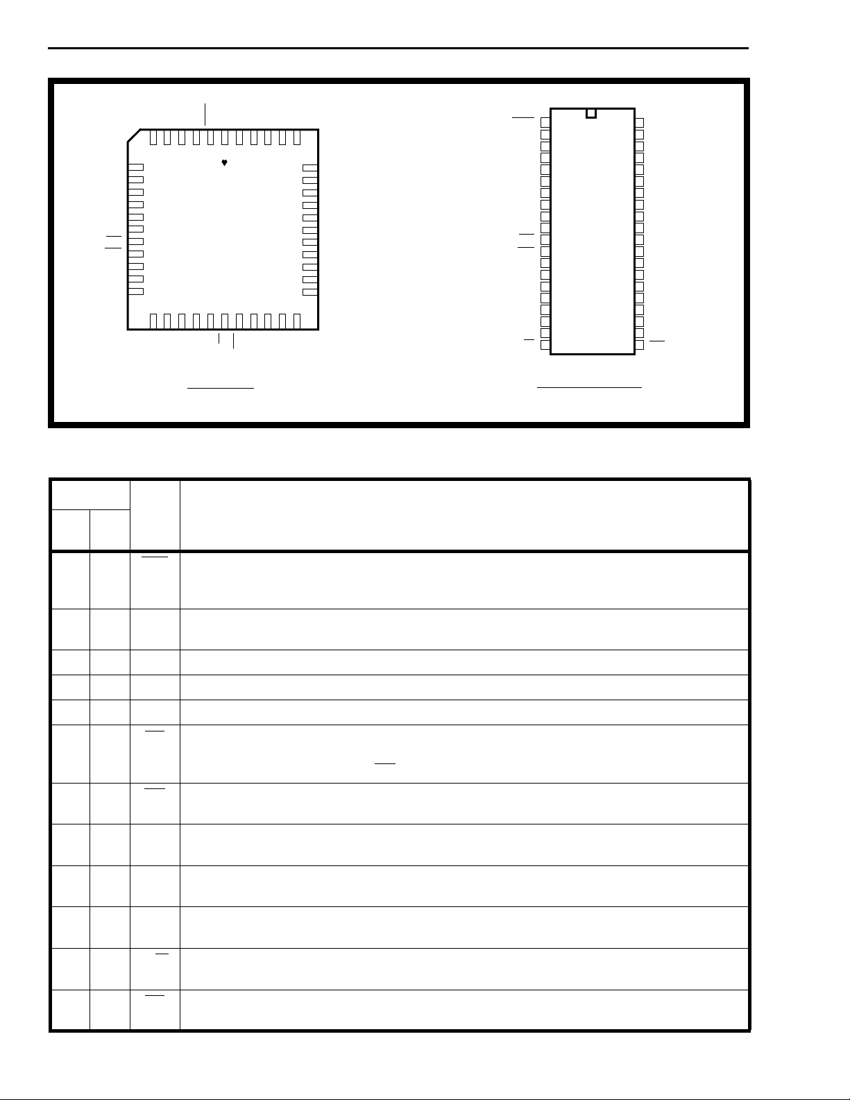
NC
65432
STi3
VDD
F0i
C4i
A0
A1
A2
7
8
IC
9
IC
10
IC
IC
11
12
13
14
15
16
17
1819202122
NC
Pin Description
Pin #
40
DIP44PLCC
Name Description
STi1
STi2
STi0
A4
A3
A5
44 PIN PLCC
DTA
ODE
IC
1
4443424140
23
2425262728
W
CS
DS
R/
STo1
STo0
D7
D6
NC
STo2
STo3
39
IC
38
IC
37
IC
36
IC
35
VSS
34
D0
33
D1
32
D2
31
D3
30
D4
29
D5
NC
Figure 2 - Pin Connections
DTA
STi0
STi1
STi2
STi3
VDD
F0i
C4i
DS
R/
1
2
3
4
5
6
IC
7
IC
8
IC
9
IC
10
11
12
13
A0
14
A1
15
A2
16
A3
17
A4
18
A5
19
20
W
40 PIN PLASTIC DIP
40
39
38
37
36
35
34
33
32
31
30
29
28
27
26
25
24
23
22
21
IC
ODE
STo0
STo1
STo2
STo3
IC
IC
IC
IC
VSS
D0
D1
D2
D3
D4
D5
D6
D7
CS
12DTA Data Acknowledgement (Open Drain Output). This is the data acknowledgement on the
microprocessor interface. This pin is pulled low to signal that the chip has processed the
data. A 909 Ω, 1/4W, resistor is recommended to be used as a pullup.
2-4 3-5 STi0-
STi2
ST-BUS Input 0 to 2 (Inputs). These are the inputs for the 2048 kbit/s ST-BUS input
streams.
5 7 STi3 ST-BUS Input 3 (Input). These are the inputs for the 2048 kbit/s ST-BUS input streams.
6-9 8-11 IC Internal Connections. Must be connected to VDD.
10 12 V
Power Input. Positive Supply.
DD
11 13 F0i Framing 0-Type (Input). This is the input for the frame synchronization pulse for the
2048 kbit/s ST-BUS streams. A low on this input causes the internal counter to reset on
the next negative transition of C4i.
12 14 C4i 4.096 MHz Clock (Input). ST-B US bit cell boundaries lie on the alternate falling edges of this
clock.
13-1515-17A0-A2 Address 0 to 2 (Inputs). These are the inputs for the address lines on the microprocessor
interface.
16-1819-21A3-A5 Address 3 to 5 (Inputs). These are the inputs for the address lines on the microprocessor
interface
19 22 DS Data Strobe (Input). This is the input for the active high data strobe on the microprocessor
interface.
20 23 R/W Read or Write (Input). This is the input for the read/write signal on the microprocessor
interface - high for read, low for write.
21 24 CS Chip Select (Input). This is the input for the active low chip select on the microprocessor
interface.
2-18
Page 3
ISO-CMOS MT8981D
Pin Description (continued)
Pin #
40
DIP44PLCC
22-2425-27D7-D5 Data 7 to 5 (Three-state I/O Pins). These are the bidirectional data pins on the
25-2929-33D4-D0 Data 4 to 0 (Three-state I/O Pins). These are the bidirectional data pins on the
Name Description
microprocessor interface.
microprocessor interface.
30 34 V
31-3435-
Power Input. Negative Supply (Ground).
SS
IC Internal Connections. Leave pins disconnected.
38
35 39 STo3 ST-BUS Output 3 (Three-state Outputs). These are the pins for the four 2048 kbit/s ST-
BUS output streams.
36-3841-43STo2-
STo0
ST-BUS Output 2 to 0 (Three-state Outputs). These are the pins for the four 2048
kbit/s ST-BUS output streams.
39 44 ODE Output Drive Enable (Input). If this input is held high, the STo0-STo3 output drivers function
normally . If this input is low, the STo0-ST o3 output driv ers go into their high impedance state.
NB: Even when ODE is high, channels on the STo0-STo3 outputs can go high impedance
under software control.
40 1 IC Internal Connection. Leave pin disconnected.
2-19
Page 4
MT8981D ISO-CMOS
Functional Description
In recent years, there has been a trend in telephony
towards digital switching, particularly in association
with software control. Simultaneously, there has
been a trend in system architectures towards
distributed processing or multi-processor systems.
In accordance with these trends, MITEL has devised
the ST-BUS (Serial Telecom Bus). This bus
architecture can be used both in software-controlled
digital voice and data switching, and for
interprocessor communications. The uses in
switching and in interprocessor communications are
completely integrated to allow for a simple general
purpose architecture appropriate for the systems of
the future.
The serial streams of the ST-BUS operate
continuously at 2048 kbit/s and are arranged in 125
µs wide frames which contain 32 8-bit channels.
MITEL manufactures a number of devices which
interface to the ST-BUS; a key device being the
MT8981 chip.
The MT8981 can switch data from channels on STBUS inputs to channels on ST-BUS outputs, and
simultaneously allows its controlling microprocessor
to read channels on ST-BUS inputs or write to
channels on ST-BUS outputs (Message Mode). To
the microprocessor, the MT8981 looks lik e a memory
peripheral. The microprocessor can write to the
MT8981 to establish switched connections between
input ST-BUS channels and output ST-BUS
channels, or to transmit messages on output ST-BUS
channels. By reading from the MT8981, the
microprocessor can receive messages from ST-BUS
input channels or check which switched connections
have already been established.
By integrating both switching and interprocessor
communications, the MT8981 allows systems to use
distributed processing and to switch voice or data in
an ST-BUS architecture.
Hardware Description
Serial data at 2048 kbit/s is received at the four STBUS inputs (STi0 to STi3), and serial data is
transmitted at the four ST-BUS outputs (STo0 to
STo3). Each serial input accepts 32 channels of
digital data, each channel containing an 8-bit word
which may represent a PCM-encoded analog/voice
sample as provided by a codec (e.g., MITEL’s
MT8964).
This serial input word is converted into parallel data
and stored in the 128 X 8 Data Memory . Locations in
the Data Memory are associated with particular
channels on particular ST-BUS input streams. These
locations can be read by the microprocessor which
controls the chip.
Locations in the Connection Memory, which is split
into high and low parts, are associated with
particular ST-BUS output streams. When a channel
is due to be transmitted on an ST-BUS output, the
data for the channel can either be switched from an
ST-BUS input or it can originate from the
microprocessor. If the data is switched from an
input, then the contents of the Connection Memory
Low location associated with the output channel is
used to address the Data Memory. This Data
Memory address corresponds to the channel on the
input ST-BUS stream on which the data for switching
arrived. If the data for the output channel originates
from the microprocessor (Message Mode), then the
contents of the Connection Memory Low location
associated with the output channel are output
directly, and this data is output repetitively on the
channel once every frame until the microprocessor
intervenes.
The Connection Memory data is received, via the
Control Interface, at D7 to D0. The Control Interface
also receives address information at A5 to A0 and
handles the microprocessor control signals CS,
DTA, R/W and DS. There are two parts to any
address in the Data Memory or Connection Memory.
The higher order bits come from the
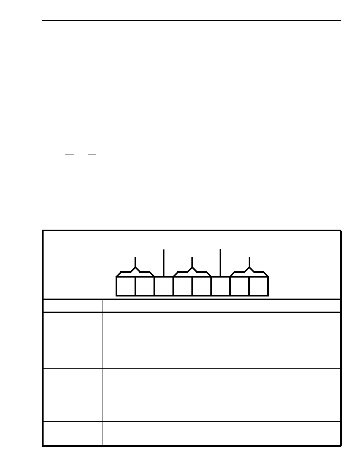
A5 A4 A3 A2 A1 A0 HEX ADDRESS LOCATION
0
1
1
•
•
•
1
* Writing to the Control Register is the only fast transaction.
† Memory and stream are specified by the contents of the Control Register.
2-20
X
0
0
•
•
•
1
X
0
0
•
•
•
1
X
0
0
•
•
•
1
X
0
0
•
•
•
1
X
0
1
•
•
•
1
Figure 3 - Address Memory Map
00 - 1F
20
21
•
•
•
3F
Control Register *
Channel 0
Channel 1
Channel 31
†
†
•
•
•
†
Page 5
ISO-CMOS MT8981D
Control Register, which may be written to or read
from via the Control Interface. The lower order bits
come from the address lines directly.
The Control Register also allows the chip to
broadcast messages on all ST-BUS outputs (i.e., to
put every channel into Message Mode), or to split the
memory so that reads are from the Data Memory
and writes are to the Connection Memory Low. The
Connection Memory High determines whether
individual output channels are in Message Mode,
and allows individual output channels to go into a
high-impedance state, which enables arrays of
MT8981s to be constructed. It also controls the
CSTo pin.
All ST-BUS timing is derived from the two
signals C4i and F0i.
Software Control
The address lines on the Control Interface give
access to the Control Register directly or, depending
on the contents of the Control Register, to the High
or Low sections of the Connection Memory or to the
Data Memory.
If address line A5 is low, then the Control Register is
addressed regardless of the other address lines (see
Fig. 3). If A5 is high, then the address lines A4-A0
select the memory location corresponding to channel
0-31 for the memory and stream selected in the
Control Register.
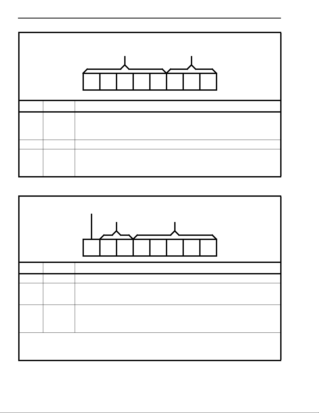
The data in the Control Register consists of mode
control bits, memory select bits, and stream address
bits (see Fig. 4). The memory select bits allow the
Connection Memory High or Low or the Data
Memory to be chosen, and the stream address bits
define one of the ST-BUS input or output streams.
Bit 7 of the Control Register allows split memory
operation - reads are from the Data Memory and
writes are to the Connection Memory Low.
The other mode control bit, bit 6, puts every output
channel on every output stream into active Message
Mode; i.e., the contents of the Connection Memory
Low are output on the ST-BUS output streams once
every frame unless the ODE pin is low. In this mode
the chip behaves as if bits 2 and 0 of every
Connection Memory High location were 1,
regardless of the actual values.
Mode
Control
Bits
76 543210
(unused)
Memory
Select
Bits
(unused)
BIT NAME DESCRIPTION
7 Split
Memory
When 1, all subsequent reads are from the Data Memory and writes are to the Connection
Memory Low, except when the Control Register is accessed again. When 0, the Memory
Select bits specify the memory for subsequent operations. In either case, the Stream
Address Bits select the subsection of the memory which is made available.
6 Message
Mode
When 1, the contents of the Connection Memory Low are output on the Serial Output
streams except when the ODE pin is low. When 0, the Connection Memory bits for each
channel determine what is output.
5 (unused)
4-3 Memory
Select Bits
0-0 - Not to be used
0-1 - Data Memory (read only from the microprocessor port)
1-0 - Connection Memory Low
1-1 - Connection Memory High
Stream
Address
Bits
2 (unused) Must be a 0.
1-0 Stream
Address
Bits
The number expressed in binary notation on these bits refers to the input or output STBUS stream which corresponds to the subsection of memory made accessible for
subsequent operations.
Figure 4 - Control Register Bits
2-21
Page 6
MT8981D ISO-CMOS
No Corresponding Memory
- These bits give 0s if read.
76 543210
76 543210
Per Channel
Control Bits
BIT NAME DESCRIPTION
2 Message
Channel
When 1, the contents of the corresponding location in Connection Memory Low are
output on the location’s channel and stream. When 0, the contents of the corresponding
location in Connection Memory Low act as an address for the Data Memory and so
determine the source of the connection to the location’s channel and stream.
1 Unused
0 Output
Enable
If the ODE pin is high and bit 6 of the Control Register is 0, then this bit enables the
output driver for the location’s channel and stream. This allows individual channels on
individual streams to be made high-impedance, allowing switching matrices to be
constructed. A 1 enables the driver and a 0 disables it.
Figure 5 - Connection Memory High Bits
(unused) Stream
Address
Bits
76 543210
Channel
Address
Bits
BIT NAME DESCRIPTION
7 (Unused) Must be a 0.
6-5* Stream
Address
Bits*
4-0* Channel
Address
Bits*
The number expressed in binary notation on these 2 bits is the number of the ST-BUS
stream for the source of the connection. Bit 6 is the most significant bit. e.g., if bit 6 is 1,
and bit 5 is 0, then the source of the connection is a channel on STi2.
The number expressed in binary notation on these 5 bits is the number of the channel
which is the source of the connection (The ST-BUS stream where the channel lies is
defined by bits 6 and 5.). Bit 4 is the most significant bit. e.g., if bit 4 is 1, bit 3 is 0, bit 2 is
0, bit 1 is 1 and bit 0 is 1, then the source of the connection is channel 19.
*If bit 2 of the corresponding Connection High location is 1 or if bit 6 of the Control Register is 1, then these entire
8 bits are output on the channel and stream associated with this location. Otherwise, the bits are used as
indicated to define the source of the connection which is output on the channel and stream associated with this
location.
Figure 6 - Connection Memory Low Bits
2-22
Page 7

ISO-CMOS MT8981D
If bit 6 of the Control Register is 0, then bits 2 and 0
of each Connection Memory High location function
normally (see Fig. 5). If bit 2 is 1, the associated STBUS output channel is in Message Mode; i.e., the
byte in the corresponding Connection Memory Low
location is transmitted on the stream at that channel.
Otherwise, one of the bytes received on the serial
inputs is transmitted and the contents of the
Connection Memory Low define the ST-BUS input
stream and channel where the byte is to be found
(see Fig. 6).
If the ODE pin is low, then all ser ial outputs are highimpedance. If it is high and bit 6 in the Control
Register is 1, then all outputs are active. If the ODE
pin is high and bit 6 in the Control Register is 0, then
the bit 0 in the Connection Memory High location
enables the output drivers for the corresponding
individual ST-BUS output stream and channel. Bit
0=1 enables the driver and bit 0=0 disables it (see
Fig. 5).
Applications
The MT8964 filter/codec in Fig. 7 receives and
transmits digitised voice signals on the ST-BUS input
DR, and ST-BUS output DX, respectively. These
signals are routed to the ST-BUS inputs and outputs
on the top MT8981, which is used as a digital speech
switch.
The MT8964 is controlled by the ST-BUS input D
originating from the bottom MT8981, which
generates the appropriate signals from an output
channel in Message Mode. This architecture
optimises the messaging capability of the line circuit
by building signalling logic, e.g., for on-off hook
detection, which communicates on an ST-BUS
output. This signalling ST-BUS output is monitored
by a microprocessor (not shown) through an ST-BUS
input on the bottom MT8981.
Fig. 8 shows how a simple digital switching system
may be designed using the ST-BUS architecture.
This is a private telephone network with 128
extensions which uses a single MT8981 as a speech
switch and a second MT8981 for communication with
the line interface circuits.
C
Use in a Simple Digital Switching System
Fig. 7 and 8 show how MT8981s can be used with
MT8964s to form a simple digital switching system.
Fig. 7 shows the interface between the MT8981s and
the filter/codecs. Fig. 8 shows the position of these
components in an example architecture.
STo0
STi0
8981 used
as
speech
switch
8981 used
in message
mode for
control and
signalling
MT8981
MT8981
STo0
STi0
A larger digital switching system may be designed by
cascading a number of MT8981s. Fig. 9 shows how
four MT8981s may be arranged in a non-blocking
configuration which can switch any channel on an y of
the ST-BUS inputs to any channel on the ST-BUS
outputs.
D
X
D
R
D
C
Line Interface Circuit with 8964 Filter/Codec
MT8964
Filter/Codec
Signalling
Logic
Line Driver
and
2- to 4-
Wire
Converter
Figure 7 - Example of Typical Interface between 8981s and 8964s for Simple Digital Switching System
2-23
Page 8

MT8981D ISO-CMOS
Line Interface Circuit
with Codec (e.g. 8964)
4
Line 1
Speech
Switch
-
8981
Controlling
Micro-
Processor
Control &
Signalling
-
8981
4
STo0-3
STo0-3
STi0-3
Figure 8 - Example Architecture of a Simple Digital Switching System
Application Circuit with 6802 Processor
Fig. 10 shows an example of a complete circuit
which may be used to evaluate the chip.
For convenience, a 4 MHz crystal oscillator has been
used rather than a 4.096 MHz clock, as both are
within the limits of the chip’s specifications. The RC
delay used with the 393 counters ensures a
sufficient hold time for the FP signal, but the values
used may have to be changed if faster 393 counters
become available.
STi0-3
•
•
4
4
Repeated for Lines
Line Interface Circuit
with Codec (e.g. 8964)
•
Repeated for Lines
2 to 127
Line 128
•
•
•
2 to 127
The chip is shown as memory mapped into the
MEK6802D3 system. Chip addresses 00-3F
correspond to processor addresses 2000-203F.
Delay through the address decoder requires the
VMA signal to be used twice to remove glitches. The
MEK6802D3 board uses a 10KΩ pullup on the MR
pin, which would have to be incorporated into the
circuit if the board was replaced by a processor.
2-24
8981
#1
IN 0/3
IN 4/7
STi0/3 STo0/3
8981
#2
STi0/3 STo0/3
8981
#3
STi0/3 STo0/3
8981
#4
STi0/3 STo0/3
OUT 0/3
OUT 4/7
Figure 9 - Four 8981s Arranged in a Non-Blocking 8 x 8 Configuration
Page 9

ISO-CMOS MT8981D
MEK6802D3
System
909 Ω,
1/4W
5V
5V
DTA
STi0
STi1
STi2
STi3
STi4
STi5
STi6
STi7
VDD
F0i
C4i
A0
A1
A2
A3
A4
A5
DS
R/W
D7-D0
A15-A0
R/
MR
VMA
E
1
2
3
4
5
6
7
8
9
10
11
12
13
14
15
16
17
18
19
20
W
MT
8980
40
39
38
37
36
35
34
33
32
31
30
29
28
27
26
25
24
23
22
21
CSTo
ODE
STo0
STo1
STo2
STo3
STo4
STo5
STo6
STo7
VSS
D0
D1
D2
D3
D4
D5
D6
D7
CS
5V
0V
A15
A14
A13
0V
0V
VMA
0V
A12
A11
A10
0V
0V
0V
A9
A8
A7
0V
0V
0V
A6
VMA
0V
0V
0V
0V
1
2
3
4
5
6
7
8
1
2
3
4
5
6
7
8
1
2
3
4
5
6
7
8
1
2
3
4
5
6
7
8
MD
74
HCT
138
MD
74
HCT
138
MD
74
HCT
138
MD
74
HCT
138
16
15
14
13
12
11
10
9
16
15
14
13
12
11
10
9
16
15
14
13
12
11
10
9
16
15
14
13
12
11
10
9
5V
5V
5V
5V
C4i
0V
0V
0V
0V
1
2
3
4
5
6
7
1
2
3
4
5
6
7
SN
74
HCT
393
SN
74
HCT
393
14
13
12
11
10
9
8
14
13
12
11
10
9
8
5V
0V
5V
510 Ω
100pF
DTA
CS
0V
C4i
0V
F0i
0V
0V
1
2
3
4
5
6
7
8
9
10
MD
74
HCT
240
4 MHz
2MΩ
20
19
18
17
16
15
14
13
12
11
5V
0V
MR
5V
Figure 10 - Application Circuit with 6802
2-25
Page 10
MT8981D ISO-CMOS
Absolute Maximum Ratings*
Parameter Symbol Min Max Units
1VDD - V
2 Voltage on Digital Inputs V
3 Voltage on Digital Outputs V
4 Current at Digital Outputs I
5 Storage Temperature T
6 Package Power Dissipation P
* Exceeding these values may cause permanent damage. Functional operation under these conditions is not implied.
SS
I
O
O
S
D
Recommended Operating Conditions - Voltages are with respect to ground (V
Characteristics Sym Min Typ
1 Operating Temperature T
2 Positive Supply V
OP
DD
3 Input Voltage V
‡ Typical figures are at 25°C and are for design aid only: not guaranteed and not subject to production testing.
-40 +85 °C
4.75 5.25 V
I
0V
DC Electrical Characteristics - Voltages are with respect to ground (V
‡
Max Units Test Conditions
DD
) unless otherwise stated.
SS
-0.3 7 V
VSS-0.3 VDD+0.3 V
VSS-0.3 VDD+0.3 V
-65 +150 °C
) unless otherwise stated.
SS
V
Characteristics Sym Min Typ‡Max Units Test Conditions
1
2 Input High Voltage V
3 Input Low Voltage V
4 Input Leakage I
5 Input Pin Capacitance C
6
7 Output High Current I
8 Output Low Voltage V
9 Output Low Current I
10 High Impedance Leakage I
11 Output Pin Capacitance C
‡ Typical figures are at 25°C and are for design aid only: not guaranteed and not subject to production testing.
Supply Current I
I
N
P
U
T
S
Output High Voltage V
O
U
T
P
U
T
S
DD
OH
OZ
IH
IL
IL
OH
OL
OL
6 10 mA Outputs unloaded
2.0 V
0.8 V
5 µAVI between VSS and V
I
8pF
2.4 V IOH = 10 mA
10 15 mA Sourcing. VOH=2.4V
0.4 V IOL = 5 mA
5 10 mA Sinking. VOL = 0.4V
5 µAVO between VSS and V
O
8pF
40 mA
2W
.
DD
DD
2-26
Output
Pin
Test Point
C
L
R
L
S1
V
SS
Figure 11 - Output Test Load
S2
V
DD
V
SS
S1 is open circuit except
when testing output levels
or high impedance states.
S2 is switched to V
when testing output
V
SS
levels or high impedance
states.
DD
or
Page 11

ISO-CMOS MT8981D
AC Electrical Characteristics† - Clock Timing (Figures 12 and 13)
Characteristics Sym Min Typ‡Max Units Test Conditions
1
2 Clock Width High t
3 Clock Width Low t
4 Clock Transition Time t
5 Frame Pulse SetupTime t
6 Frame Pulse Hold Time t
7 Frame Pulse Width t
† Timing is over recommended temperature & power supply voltages
‡ Typical figures are at 25°C and are for design aid only: not guaranteed and not subject to production testing.
* Contents of Connection Memory are not lost if the clock stops, however, ST-BUS outputs go into the high impedance state.
NB: Frame Pulse is repeated ever y 512 cycles of C4i.
C4i
F0i
BIT
CELLS
Clock Period* t
I
N
P
U
T
S
Channel 31
Bit o
CLK
CH
CL
CTT
FPS
FPH
FPW
220 244 300 ns
95 122 150 ns
110 122 150 ns
20 ns
20 200 ns
0.020 50 µs
244 ns
Channel 0
Bit 7
C4i
F0i
2.0V
0.8V
2.0V
0.8V
t
FPH
Figure 12 - Frame Alignment
t
CLK
t
CL
t
t
CTT
FPS
t
CHL
t
FPW
t
CTT
t
FPH
t
CH
t
FPS
Figure 13 - Clock Timing
2-27
Page 12

MT8981D ISO-CMOS
AC Electrical Characteristics† - Serial Streams (Figures 11, 14, 15 and 16)
Characteristics Sym Min Typ‡Max Units Test Conditions
1
2 STo0/3 Delay - High Z to Active t
3 STo0/3 Delay - Active to Active t
4 STo0/3 Hold Time t
5 Output Driver Enable Delay t
6 External Control Hold Time t
7 External Control Delay t
8
9 Serial Input Hold Time t
† Timing is over recommended temperature & power supply voltages
‡ Typical figures are at 25
* High Impedance is measured by pulling to the appropriate rail with RL, with timing corrected to cancel time taken to discharge CL.
C4i
STo0/3 Delay - Active to High Z t
O
U
T
P
U
T
S
Serial Input Setup Time t
I
N
°C and are for design aid only: not guaranteed and not subject to production testing.
Bit Cell Boundary
2.0V
0.8V
SAZ
SZA
SAA
SOH
OED
XCH
XCD
SIS
SIH
20 50 80 ns RL=1 KΩ*, CL=150 pF
25 60 125 ns CL=150 pF
30 65 125 ns CL=150 pF
25 45 ns CL=150 pF
45 125 ns RL=1 KΩ*, CL=150 pF
050 nsC
=150 pF
L
75 110 ns CL=150 pF
-40 -20 ns
90 ns
2.0V
ODE
0.8V
STo0
to
STo3
STo0
to
STo3
STo0
to
STo3
2.4V
0.4V
2.4V
0.4V
2.4V
0.4V
t
SOH
2.4V
STo0
to
STo3
0.4V
t
*
SAZ
*
t
SZA
t
SOH
2.0V
C4i
STi0
to
STi3
0.8V
2.0V
0.8V
t
SAA
*
t
OED
t
OED
Figure 15 - Output Driver Enable
Bit Cell Boundaries
t
SIS
t
*
SIH
Figure 14 - Serial Outputs and External Control
2-28
Figure 16 - Serial Inputs
Page 13

ISO-CMOS MT8981D
AC Electrical Characteristics† - Processor Bus (Figures 11 and 17)
Characteristics Sym Min Typ
‡
Max Units Test Conditions
1 Chip Select Setup Time t
2 Read/Write Setup Time t
3 Address Setup Time t
4 Acknowledgement Delay Fast
Slow
5 Fast Write Data Setup Time t
6 Slow Write Data Delay t
7 Read Data Setup Time t
8 Data Hold Time Read
Write
9 Read Data To High Impedance t
10 Chip Select Hold Time t
11 Read/Write Hold Time t
12 Address Hold Time t
13 Acknowledgement Hold Time t
† Timing is over recommended temperature & power supply voltages.
‡ Typical figures are at 25°C and are for design aid only: not guaranteed and not subject to production testing.
* High Impedance is measured by pulling to the appropriate rail with RL, with timing corrected to cancel time taken to discharge CL.
CSS
RWS
ADS
t
AKD
t
AKD
FWS
SWD
RDS
t
DHT
t
DHT
RDZ
CSH
RWH
ADH
AKH
20 0 ns
25 5 ns
25 5 ns
40 100 ns CL=150 pF
2.7 7.2 cycles C4i cycles
➀
20 ns
2.0 1.7 cycles C4i cycles
➀
0.5 cycles C4i cycles➀, CL= 150 pF
20 ns RL=1 KΩ∗, CL=150 pF
20 10 ns
50 90 ns RL=1 KΩ∗, CL=150 pF
0ns
0ns
0ns
10 60 80 ns RL=1 KΩ∗, CL=150 pF
➀ Processor accesses are dependent on the C4i clock, and so some timings are expressed as multiples of the C4i clock period.
DS
CS
W
R/
A5
to
A0
DTA
D7
to
D0
2.0V
0.8V
2.0V
0.8V
t
CSS
2.0V
0.8V
t
RWS
2.0V
0.8V
t
ADS
2.4V
*
0.4V
2.4V (Read) 2.0V (Write)
0.8V (Read 0.8V (Write)
t
CSH
t
RWH
t
t
AKD
t
AKH
ADH
*
t
RDS
*
t
t
SWD
FWS
t
DHT
t
*
RDZ
Figure 17 - Processor Bus
2-29
Page 14

MT8981D ISO-CMOS
Notes:
2-30
Page 15

Package Outlines
F
D
1
D
H
E
E
1
e: (lead coplanarity)
A
1
I
E
2
Notes:
1) Not to scale
2) Dimensions in inches
3) (Dimensions in millimeters)
4) For D & E add for allowable Mold Protrusion 0.010"
A
G
D
2
Dim
A
A
D/E
D1/E
D2/E
e
F
G
H
I
20-Pin 28-Pin 44-Pin 68-Pin 84-Pin
Min Max Min Max Min Max Min Max Min Max
0.165
(4.20)
0.090
1
(2.29)
0.385
(9.78)
0.350
1
(8.890)
0.290
2
(7.37)
0.026
(0.661)
0.013
(0.331)
0.020
(0.51)
0.180
(4.57)
0.120
(3.04)
0.395
(10.03)
0.356
(9.042)
0.330
(8.38)
0 0.004 0 0.004 0 0.004 0 0.004 0 0.004
0.032
(0.812)
0.021
(0.533)
0.050 BSC
(1.27 BSC)
0.165
(4.20)
0.090
(2.29)
0.485
(12.32)
0.450
(11.430)
0.390
(9.91)
0.026
(0.661)
0.013
(0.331)
0.050 BSC
(1.27 BSC)
0.020
(0.51)
0.180
(4.57)
0.120
(3.04)
0.495
(12.57)
0.456
(11.582)
0.430
(10.92)
0.032
(0.812)
0.021
(0.533)
0.165
(4.20)
0.090
(2.29)
0.685
(17.40)
0.650
(16.510)
0.590
(14.99)
0.026
(0.661)
0.013
(0.331)
0.050 BSC
(1.27 BSC)
0.020
(0.51)
0.180
(4.57)
0.120
(3.04)
0.695
(17.65)
0.656
(16.662)
0.630
(16.00)
0.032
(0.812)
0.021
(0.533)
0.165
(4.20)
0.090
(2.29)
0.985
(25.02)
0.950
(24.130)
0.890
(22.61)
0.026
(0.661)
0.013
(0.331)
0.050 BSC
(1.27 BSC)
0.020
(0.51)
0.200
(5.08)
0.130
(3.30)
0.995
(25.27)
0.958
(24.333)
0.930
(23.62)
0.032
(0.812)
0.021
(0.533)
(30.10)
(29.210)
(27.69)
(0.661)
(0.331)
0.165
(4.20)
0.090
(2.29)
1.185
1.150
1.090
0.026
0.013
0.050 BSC
(1.27 BSC)
0.020
(0.51)
0.200
(5.08)
0.130
(3.30)
1.195
(30.35)
1.158
(29.413)
1.130
(28.70)
0.032
(0.812)
0.021
(0.533)
General-10
Plastic J-Lead Chip Carrier - P-Suffix
Page 16

Package Outlines
E
1
D
32
n-2 n-1 n
1
E
L
Notes:
1) Not to scale
2) Dimensions in inches
3) (Dimensions in millimeters)
A
b
D
1
e
2
b
A
2
Plastic Dual-In-Line Packages (PDIP) - E Suffix
8-Pin 16-Pin 18-Pin 20-Pin
DIM
Plastic Plastic Plastic Plastic
Min Max Min Max Min Max Min Max
A
A
2
b
b
2
C
D
D
1
E
E
1
e
e
A
L
e
B
e
C
NOTE: Controlling dimensions in parenthesis ( ) are in millimeters.
0.115 (2.92) 0.195 (4.95) 0.115 (2.92) 0.195 (4.95) 0.115 (2.92) 0.195 (4.95) 0.115 (2.92) 0.195 (4.95)
0.014 (0.356) 0.022 (0.558) 0.014 (0.356) 0.022 (0.558) 0.014 (0.356) 0.022 (0.558) 0.014 (0.356) 0.022 (0.558)
0.045 (1.14) 0.070 (1.77) 0.045 (1.14) 0.070 (1.77) 0.045 (1.14) 0.070 (1.77) 0.045 (1.14) 0.070 (1.77)
0.008
(0.203)
0.355 (9.02) 0.400 (10.16) 0.780 (19.81) 0.800 (20.32) 0.880 (22.35) 0.920 (23.37) 0.980 (24.89) 1.060 (26.9)
0.005 (0.13) 0.005 (0.13) 0.005 (0.13) 0.005 (0.13)
0.300 (7.62) 0.325 (8.26) 0.300 (7.62) 0.325 (8.26) 0.300 (7.62) 0.325 (8.26) 0.300 (7.62) 0.325 (8.26)
0.240 (6.10) 0.280 (7.11) 0.240 (6.10) 0.280 (7.11) 0.240 (6.10) 0.280 (7.11) 0.240 (6.10) 0.280 (7.11)
0.100 BSC (2.54) 0.100 BSC (2.54) 0.100 BSC (2.54) 0.100 BSC (2.54)
0.300 BSC (7.62) 0.300 BSC (7.62) 0.300 BSC (7.62) 0.300 BSC (7.62)
0.115 (2.92) 0.150 (3.81) 0.115 (2.92) 0.150 (3.81) 0.115 (2.92) 0.150 (3.81) 0.115 (2.92) 0.150 (3.81)
0 0.060 (1.52) 0 0.060 (1.52) 0 0.060 (1.52) 0 0.060 (1.52)
0.210 (5.33) 0.210 (5.33) 0.210 (5.33) 0.210 (5.33)
0.014 (0.356) 0.008 (0.203) 0.014(0.356) 0.008 (0.203) 0.014 (0.356) 0.008 (0.203) 0.014 (0.356)
0.430 (10.92) 0.430 (10.92) 0.430 (10.92) 0.430 (10.92)
C
e
A
e
B
e
C
General-8
Page 17

E
1
L
Notes:
1) Not to scale
2) Dimensions in inches
3) (Dimensions in millimeters)
Package Outlines
32
1
E
n-2 n-1 n
D
A
b
D
1
e
2
b
A
2
C
e
A
e
B
Plastic Dual-In-Line Packages (PDIP) - E Suffix
α
DIM
A
A
b
b
C
D
D
E
E
E
E
e
e
A
e
A
e
B
L
α
22-Pin 24-Pin 28-Pin 40-Pin
Plastic Plastic Plastic Plastic
Min Max Min Max Min Max Min Max
0.210 (5.33) 0.250 (6.35) 0.250 (6.35) 0.250 (6.35)
2
2
1
1
1
0.125 (3.18) 0.195 (4.95) 0.125 (3.18) 0.195 (4.95) 0.125 (3.18) 0.195 (4.95) 0.125 (3.18) 0.195 (4.95)
0.014 (0.356) 0.022 (0.558) 0.014 (0.356) 0.022 (0.558) 0.014 (0.356) 0.022 (0.558) 0.014 (0.356) 0.022 (0.558)
0.045 (1.15) 0.070 (1.77) 0.030 (0.77) 0.070 (1.77) 0.030 (0.77) 0.070 (1.77) 0.030 (0.77) 0.070 (1.77)
0.008 (0.204) 0.015 (0.381) 0.008 (0.204) 0.015 (0.381) 0.008 (0.204) 0.015 (0.381) 0.008 (0.204) 0.015 (0.381)
1.050 (26.67) 1.120 (28.44) 1.150 (29.3) 1.290 (32.7) 1.380 (35.1) 1.565 (39.7) 1.980 (50.3) 2.095 (53.2)
0.005 (0.13) 0.005 (0.13) 0.005 (0.13) 0.005 (0.13)
0.390 (9.91) 0.430 (10.92) 0.600 (15.24) 0.670 (17.02) 0.600 (15.24) 0.670 (17.02) 0.600 (15.24) 0.670 (17.02)
0.290 (7.37) .330 (8.38)
0.330 (8.39) 0.380 (9.65) 0.485 (12.32) 0.580 (14.73) 0.485 (12.32) 0.580 (14.73) 0.485 (12.32) 0.580 (14.73)
0.246 (6.25) 0.254 (6.45)
0.100 BSC (2.54) 0.100 BSC (2.54) 0.100 BSC (2.54) 0.100 BSC (2.54)
0.400 BSC (10.16) 0.600 BSC (15.24) 0.600 BSC (15.24) 0.600 BSC (15.24)
0.300 BSC (7.62)
0.430 (10.92)
0.115 (2.93) 0.160 (4.06) 0.115 (2.93) 0.200 (5.08) 0.115 (2.93) 0.200 (5.08) 0.115 (2.93) 0.200 (5.08)
15° 15° 15° 15°
Shaded areas for 300 Mil Body Width 24 PDIP only
Page 18

http://www.mitelsemi.com
World Headquarters - Canada
Tel: +1 (613) 592 2122
Fax: +1 (613) 592 6909
North America Asia/Pacific Europe, Middle East,
Tel: +1 (770) 486 0194 Tel: +65 333 6193 and Africa (EMEA)
Fax: +1 (770) 631 8213 Fax: +65 333 6192 Tel: +44 (0) 1793 518528
Fax: +44 (0) 1793 518581
Information relating to products and services furnished herein by Mitel Corporation or its subsidiaries (collectively “Mitel”) is believed to be reliable. However, Mitel assumes no
liability for errors that may appear in this publication, or for liability otherwise arising from the application or use of any such information, product or service or for any infringement of
patents or other intellectual property rights owned by third parties which may result from such application or use. Neither the supply of such information or purchase of product or
service conveys any license, either express or implied, under patents or other intellectual property rights owned by Mitel or licensed from third parties by Mitel, whatsoever.
Purchasers of products are also hereby notified that the use of product in certain ways or in combination with Mitel, or non-Mitel furnished goods or services may infringe patents or
other intellectual property rights owned by Mitel.
This publication is issued to provide information only and (unless agreed by Mitel in writing) may not be used, applied or reproduced for any pur pose nor form par t of any order or
contract nor to be regarded as a representation relating to the products or services concerned. The products, their specifications, services and other information appearing in this
publication are subject to change by Mitel without notice. No warranty or guarantee express or implied is made regarding the capability, perfor mance or suitability of any product or
service. Information concerning possible methods of use is provided as a guide only and does not constitute any guarantee that such methods of use will be satisfactory in a specific
piece of equipment. It is the user’s responsibility to fully determine the performance and suitability of any equipment using such information and to ensure that any publication or
data used is up to date and has not been superseded. Manufacturing does not necessarily include testing of all functions or parameters. These products are not suitable for use in
any medical products whose failure to perform may result in significant injury or death to the user. All products and materials are sold and services provided subject to Mitel’s
conditions of sale which are available on request.
M Mitel (design) and ST-BUS are registered trademarks of MITEL Corporation
Mitel Semiconductor is an ISO 9001 Registered Company
Copyright 1999 MITEL Corporation
All Rights Reserved
Printed in CANADA
TECHNICAL DOCUMENTATION - NOT FOR RESALE
 Loading...