

Page 1
ISO-CMOS ST-BUS FAMILY
MT8952B
HDLC Protocol Controller
Features
• Formats data as per X.25 (CCITT) level-2
standards
• Go-Ahead sequence generation and detection
• Single byte address recognition
• Microprocessor port and directly accessible
registers for flexible operation and control
• 19 byte FIFO in both send and receive paths
• Handshake signals for multiplexing data links
• High speed serially clocked output (2.5 Mbps)
• ST-BUS compatibility with programmable
channel selection for data and separate
timeslot for control information
• Independent watchdog timer
• Facility to disable protocol functions
• Low power ISO-CMOS technology
Applications
• Data link controllers and protocol generators
• Digital sets, PBXs and private packet networks
• D-channel controller for ISDN basic access
• C-channel controller to Digital Network
Interface Circuits (typically MT8972)
• Interprocessor communication
ISSUE 5 May 1995
Ordering Information
MT8952BC 28 Pin Ceramic DIP
MT8952BE 28 Pin Plastic DIP
MT8952BP 28 Pin PLCC
MT8952BS 28 Pin SOIC
-40°C to 85°C
Description
The MT8952B HDLC Protocol Controller frames and
formats data packets according to X.25 (Level 2)
Recommendations from the CCITT.
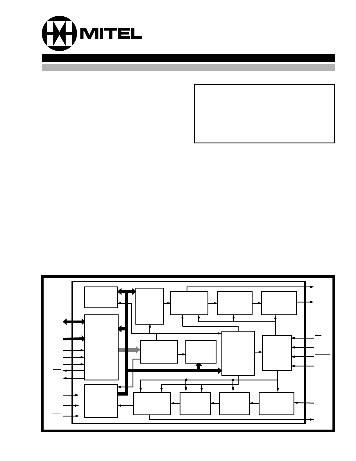
D0-D7
A0-A3
R/
CS
IRQ
WD
V
DD
V
SS
RST
TEOP
C-Channel
Interface
Micro
Processor
W
E
Interface
Receive
FIFO
Transmit
FIFO
Address
Decoder
Receive Logic
Transmit
Logic
Interrupt
Registers
Address
Detection
Zero
Insertion
Control
and Status
Register
Zero
Deletion
Flag/Abort
Generator
Timing
Logic
Flag/Abort/
Idle
Detection
CDSTo
F0i
CKi
RxCEN
TxCEN
CDSTi
REOP
Figure 1 - Functional Block Diagram
3-61
Page 2
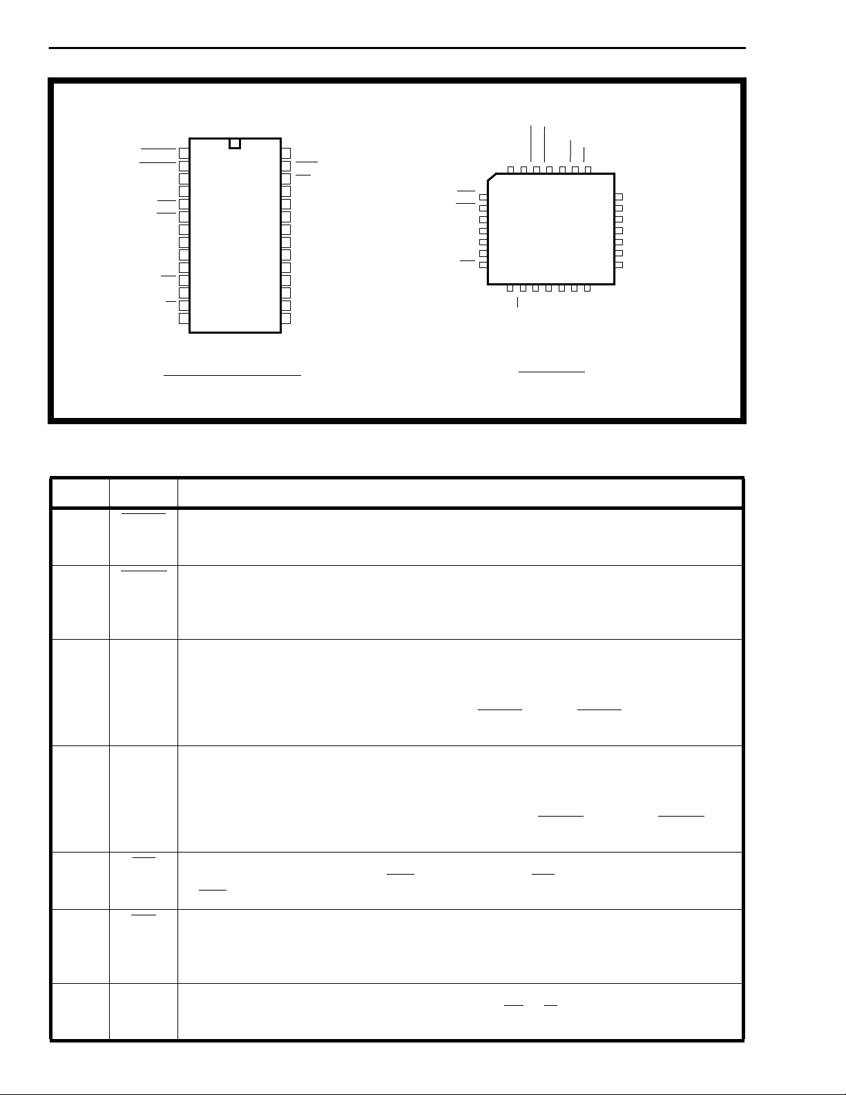
MT8952B ISO-CMOS
TxCEN
RxCEN
CDSTo
CDSTi
R/
VSS
1
2
3
4
5
WD
6
IRQ
7
A0
8
A1
9
A2
10
A3
11
CS
12
E
13
W
14
28 PIN PDIP/CERDIP/SOIC
28
27
26
25
24
23
22
21
20
19
18
17
16
15
VDD
RST
F0i
CKi
TEOP
REOP
D7
D6
D5
D4
D3
D2
D1
D0
WD
IRQ
A0
A1
A2
A3
CS
CDSTi
4
5
6
7
8
9
10
11
12
E
28 PIN PLCC
CDSTo
RxCEN
3
2
•
13
14
W
R/
VSS
TxCEN
VDD
1
28
15
16
D1
D0
RST
27
17
D2
F0i
26
18
D3
25
24
23
22
21
20
19
CKi
TEOP
REOP
D7
D6
D5
D4
Figure 2 - Pin Connections
Pin Description
Pin No. Name Description
1 TxCEN T ransmit Cloc k Enable -This active LOW input enab les the transmit section in the External
Timing Mode. When LOW, CDSTo is enabled and when HIGH, CDSTo is in high impedance
state. If the Protocol Controller is in the Internal Timing Mode, this input is ignored.
2 RxCEN Receive Clock Enable - This active LOW input enables the receive section in the External
Timing Mode. When LOW, CDSTi is enabled and when HIGH, the clock to the receive
section is inhibited. If the Protocol Controller is in the Internal Timing Mode, this input is
ignored.
3 CDSTo C and D channel Output in ST-BUS format - This is the serial formatted data output from
the transmitter in NRZ form. It is in ST-BUS format if the Protocol Controller is in Internal
Timing Mode with the data in selected timeslots (0,2,3 and 4) and the C-channel information
in timeslot No. 1. If the Protocol Controller is in External Timing Mode, the formatted data is
output on the rising edge of the clock (CKi) when TxCEN LOW . IfTxCEN is HIGH, CDSTo is
in high impedance state.
4 CDSTi C and D channel Input in ST-BUS format - This is the serial formatted data input to the
receiver in NRZ form. It must be in ST-BUS format if the Protocol Controller is in Internal
Timing Mode with the input data in selected timeslots (0,2,3 and 4) and the C-channel
information in timeslot No.1. If the Controller is in External Timing Mode, the serial input
data is sampled on the falling edge of the clock CKi when RxCEN is LOW. If RxCEN is
HIGH, the clock to receive section is inhibited.
5 WD Watch-Dog Timer output - Normally a HIGH lev el output, going LO W if the Watchdog timer
times out or if the external reset (RST) is held LOW. The WD output remains LOW as long
as RST is held LOW.
6 IRQ Interrupt Request Output (Open Drain) - This active LOW output notifies the controlling
microprocessor of an interrupt request. It goes LOW only when the bits in the Interrupt
Enable Register are programmed to acknowledge the source of the interrupt as defined in
the Interrupt Flag Register.
7-10 A0-A3 Address Bus Inputs - These bits address the various registers in the Protocol Controller.
They select the internal registers in conjunction with CS, R/W inputs and E Clock. (Refer to
Table 1.)
3-62
Page 3

ISO-CMOS MT8952B
Pin Description (continued)
Pin No. Name Description
11 CS Chip Select Input - This is an active LOW input enabling the Read or Write operation to
various registers in the Protocol Controller.
12 E Enable Clock Input - This input activates the Address Bus and R/W input and enables
data transfers on the Data Bus.
13 R/W Read/Write Control - This input controls the direction of data flow on the data bus. When
HIGH, the I/O buffer acts as an output driver and as an input buffer when LOW.
14 V
15-22 D0-D7 Bidirectional Data Bus - These Data Bus I/O ports allow the data transfer between the
23 REOP Receive End Of Packet (Output) - This is a HIGH going pulse that occurs for one bit
24 TEOP Transmit End Of Packet (Output) - This is a HIGH going pulse that occurs for one bit
25 CKi Clock Input (Bit rate clock or 2 x bit rate clock in ST-BUS format while in the Internal
26 F0i Frame Pulse Input - This is the frame pulse input in ST-BUS format to establish the
27 RST RESET Input - This is an active LOW Schmitt Trigger input, resetting all the registers
28 V
Ground (0 Volt).
SS
HDLC Protocol Controller and the microprocessor.
duration when a closing flag is detected on the incoming packets, or the incoming packet is
aborted, or when an invalid packet of 24 or more bits is received.
duration when a packet is transmitted correctly or aborted.
Timing Mode and bit rate Clock in the External Timing Mode) - This is the clock input
used for shifting in/out the formatted packets. It can be at bit rate (C2i) or twice the bit rate
(C4i) in ST-BUS format while the Protocol Controller is in the Internal Timing Mode.
Whether the clock should be C2i (typically 2.048 MHz) or C4i (typically 4.096 MHz) is
decided by the BRCK bit in the Timing Control Register. If the Protocol Controller is in the
External Timing Mode, it is at the bit rate.
beginning of the frame in the Internal Timing Mode. This is also the signal clocking the
watchdog timer.
including the transmit and receive FIFOs and the watchdog timer.
Supply (5 Volts).
DD
Address Bits Registers
A3 A2 A1 A0 Read Write
0 0 0 0 FIFO Status 0 0 0 1 Receive Data Transmit Data 0 0 1 0 Control Control 0 0 1 1 Receive Address Receive Address 0 1 0 0 C-Channel Control (Transmit) C-Channel Control (Transmit) 0 1 0 1 Timing Control Timing Control 0 1 1 0 Interrupt Flag Watchdog Timer 0 1 1 1 Interrupt Enable Interrupt Enable 1 0 0 0 General Status 1 0 0 1 C-Channel Status (Receive) -
Table 1. Register Addresses
3-63
Page 4

MT8952B ISO-CMOS
Introduction
The MT8952B HDLC Protocol Controller handles bit
oriented protocol structure and formats the data as
per the packet switching protocol defined in the X.25
(Level 2) recommendations of the CCITT. It
transmits and receives the packeted data
(information or control) serially in a format shown in
Figure 3 , while providing the data transparency by
zero insertion and deletion. It generates and detects
the flags, various link channel states and the abort
sequence. Further, it provides a cyclic redundancy
check on the data packets using the CCITT defined
polynomial. In addition, it can generate and detect a
Go Ahead sequence and recognize a single byte
address in the received frame. There is also a
provision to disable the protocol functions and
provide transparent access to the serial bus through
the parallel port.
Frame Format
All frames start with an opening flag and end with a
closing flag as shown in Figure 3. Between these
two flags, a frame contains the data and the frame
check sequence (FCS).
FLAG DATA FIELD FCS FLAG
One Byte
n Bytes
(n ≥ 2)
Figure 3. Frame Format
Two
Bytes
One
Byte
address detection can be limited only to the upper
six bits by setting HIGH both RA6/7 and RxAD bits in
the Control Register.
Frame Check Sequence (FCS):
The 16 bits following the data field are the frame
check sequence bits. The generator polynomial is:
G(x)=x16+x12+x5+1
The transmitter calculates the FCS on all bits of the
data field and transmits after the data field and
before the end flag. The receiver performs a similar
computation on all bits of the received data and FCS
fields and the result is compared with FOB8
matches, the received data is assumed error free.
The error status of the received packet is indicated
by D7 and D6 bits in the FIFO Status Register.
Zero Insertion and Deletion:
The Protocol Controller, while sending either data
from the FIFO or the 16 bits FCS, checks the
transmission on a bit-by-bit basis and inserts a
ZERO after every sequence of five contiguous ONEs
(including the last five bits of FCS) to ensure that the
flag sequence is not simulated. Similarly the
receiver examines the incoming frame content and
discards any ZERO directly following the five
contiguous ONEs.
Abort:
Hex
. If it
Flag:
The flag is a unique pattern of 8 bits (01111110)
defining the frame boundary. The transmit section
generates the flags and appends them automatically
to the frame to be transmitted. The receive section
searches the incoming packets for flags on a bit-bybit basis and establishes frame synchronization. The
flags are used only to identify and synchronize the
received frame and are not transferred to the FIFO.
Data:
The data field refers to the Address, Control and
Information fields defined in the CCITT
recommendations. A valid frame should have a data
field of at least 16 bits. The first byte in the data field
is the address of the frame. If RxAD bit in the
Control Register is HIGH, the incoming packet is
recognized only if the address byte matches the byte
stored in the Receive Address Register or the
address byte is the All-Call Address (all ONEs). The
LSB of the Receive Address Register is set LOW
permanently and the comparison is done only on
upper seven bits of the received address byte. The
The transmitter aborts a frame by sending eight
consecutive ONEs. The FA bit in the Control
Register along with a write operation to the Transmit
Data Register enables the transmission of abort
sequence instead of the byte written to the register.
On the receive side, the ABRT bit in the General
Status Register is set whenever an abort sequence
(7 or more continuous 1’s) is received. The abort
sequence causes the receiver to abandon whatever
it was doing and start searching for a start flag. The
FA bit in the Interrupt Status Register is set when an
abort sequence is received following a start flag and
at least four data bytes (minimum for a valid frame).
Interframe Time Fill and Link Channel States
When the HDLC Protocol Controller is not sending
packets, the transmitter can be in any of three states
mentioned below depending on the status of the
IFTF0 and IFTF1 bits in the Control Register. These
bits are also used to disable the protocol function to
provide the transparent parallel access to the serial
bus through the microprocessor port.
3-64
Page 5

ISO-CMOS MT8952B
Idle state:
The Idle state is defined as 15 or more contiguous
ONEs. When the HDLC Protocol Controller is
observing this condition on the receiving channel,
the Idle bit in the General Status Register is set
HIGH. On the transmit side, the Protocol Controller
ends the Idle state when data is loaded into the
transmit FIFO.
Interframe time fill state:
The Protocol Controller transmits continuous flags
(7E
) in Interframe time fill state and ends this
Hex
state when data is loaded into the transmit FIFO.
Go Ahead state:
Go Ahead is defined by the 9 bit sequence
011111110 (7F
contiguous 7F’s appear as Go Aheads. Once the
transmitter is in ‘Go Ahead’ state, it will continue to
remain so even after the data is loaded into the
FIFO. This state can only be changed by setting the
IFTF bits in the Control Register to something other
than ‘GO Ahead’. The reception of this sequence is
indicated by GA bit in the General Status Register
and the Protocol Controller can generate an interrupt
if enabled to do so by the GA bit in the Interrupt
Enable Register.
followed by a ZERO), and hence
Hex
The serial port can be configured to operate in two
modes depending on the IC bit in the Timing Control
Register. It can transmit/receive the packets on
selected timeslots in ST- BUS format or it can,
using the enable signals (TxCEN and RxCEN),
transmit/receive the packets at a bit rate equal to CKi
clock input.
The microprocessor port allows parallel data
transfers between the Protocol Controller and a
6800/6809 system bus. This interface consists of
Data Bus (D0-D7), Address Bus (A0-A3), E Clock,
Chip Select (CS) and R/W control. The microprocessor can read and write to the various registers
in the Protocol Controller. The addresses of these
registers are given in Table 2. The IRQ is an open
drain, active LOW output indicating an interrupt
request to CPU. Control and monitoring of many
different interrupts that may originate from the
protocol controller is implemented by the Interrupt
Flag Register (IFR) and the Interrupt Enable
Register (IER). Specific events have been described
that set a bit HIGH in the Interrupt Flag Register.
Such an event does not necessarily interrupt the
CPU. To assert an interrupt (pull IRQ output LOW)
the bit in IER that coincides with the Interrupt Flag
Register must be set HIGH. The IRQ bit in the
General Status Register is the complement of IRQ
pin status. If an interrupt is asserted, this bit will be
set HIGH otherwise it will be LOW.
Transparent Data Transfer State:
The Protocol Controller, in this state, disables the
protocol functions defined earlier and provides bidirectional access to the serial bit streams through
the parallel port. Like other states, the transparent
data transfer can be selected in both timing modes.
Invalid Frames
Any frame shorter than 32 bits between the opening
and closing flags (corresponding to 16 bits of data
and 16 bits FCS) is considered invalid. The Protocol
Controller ignores the frame only if the frame length
is less than 24 bits between the flags. For frames of
length 24 to 32 bits, it transfers the data field to FIFO
and tags it as having bad FCS in the FIFO Status
Register.
Functional Description
The functional block diagram of the HDLC Protocol
Controller is shown in Figure 1. It has two ports.
The serial port transmits and receives formatted data
packets and the parallel port provides a
microprocessor interface for access to various
registers in the Protocol Controller.
TEOP and REOP Outputs:
The HDLC Protocol Controller provides two separate
signals TEOP & REOP indicating the end of packet
transmitted and received respectively. TEOP is a
HIGH going pulse for one bit duration asserted
during the last bit of the closing flag or Abort
sequence of the transmit packet. REOP is also a
HIGH going pulse occurring for one bit period when
a closing flag is received or an incoming packet is
aborted or an invalid packet of 24 or more bits is
detected. However, REOP is not generated for
invalid packets of length less than 24 bits. These
‘end of packet’ signals are useful in multiplexing
several data links on to a single HDLC Protocol
Controller.
Timing Modes
There are two timing modes the Protocol Controller
can be run in. These timing modes refer only to the
configuration of the serial port and are not related to
the microprocessor port.
Internal Timing Mode
The Internal Timing Mode is intended for an easy
interface to various products using ST-BUS
3-65
Page 6

MT8952B ISO-CMOS
architecture, particularly MITEL’s Digital Network
Interface Circuit (DNIC - MT8972). The data/packets
are shifted in/out serially in ST-BUS format using the
timing signals F0i and C2i/C4i. In addition to framing
the data, the Protocol Controller reserves one
channel (channel-1) on the ST-BUS for carrying
control information (C-channel) and this timeslot can
not be used for the packetized data. While the
Protocol Controller is in the Internal Timing Mode,
the clock input CKi can be either at the bit rate or at
2bit rate depending on the BRCK bit in the Timing
Control Register as shown in Table 2.
BRCK Bit CKi Input
0 4.096 MHz/C4i 2.048 Mbps 1 2.048 MHz/C2i 2.048 Mbps
Table 2. Output Bit Rate In Internal Timing Mode
The Protocol Controller uses the ST-BUS timing
signals F0i and C2i/C4i, and enables the transmitter
and receiver sections in the appropriate timeslots
as determined by TC0-TC3 bits in the Timing
Control Register.
The TxCEN and RxCEN inputs are ignored in this
mode.
C-Channel Interface
This is a separate control channel (C-channel)
interface relevant only in the Internal Timing Mode.
The data stored in the C-Channel Control Register is
shifted out during the channel-1 timeslot of the
outgoing ST-BUS (CDSTo) and the C1EN bit in the
Timing Control Register enables the transmission.
The transmission of C-Channel is independent of
packet/data transmission. The data received on
channel-1 of the incoming ST-BUS (CDSTi) is shifted
into the C-Channel Status Register independently
and it is updated continuously.
Both the C-channel registers are accessible by the
accompanying CPU through the parallel port.
External Timing Mode
In the External Timing Mode, the transmit and
receive sections are enabled independently by
TxCEN and RxCEN control inputs and the formatted
data packets are shifted in/out serially at a rate equal
to the clock frequency on CKi. The output is
transmitted on the rising edge and the receiver
samples the input on the falling edge of the clock.
The TxCEN and RxCEN controls are independent
Output Data
Rate
and asynchronous and have effect only after the
current bit in the packet is transmitted/received.
Although the protocol controller provides the
packetized data on a limited number of channels on
the ST-BUS while operating in the Internal Timing
Mode, it can packetize the data on any or all the
channels of the ST-BUS if it is operated in the
External Timing Mode with appropriate enable
signals on TxCEN and RxCEN.
Transparent Data Transfer
By setting the IFTF bits in the Control Register
appropriately, the protocol functions can be disabled.
This provides a bidirectional access to the serial port
through the microprocessor interface, with 19 byte
deep FIFO in each direction. The transparent data
transfer facility functions in bytewide format and is
available in both timing modes except when the
timing control bits are set for one bit/frame during the
Internal Timing Mode.
The transmit data is shifted out serially on CDSTo
and the operation being bytewide, only the least
significant bits of each byte loaded are transmitted, if
the timing control bits are set to select 2, 6 or 7 bits/
frame. When the transmit FIFO is empty, the last
byte or the portion the last byte, written to the FIFO
is transmitted repeatedly. Similarly the serial data on
CDSTi is shifted in and converted to bytewide
format. In case the timeslot selected is 2, 6 or 7 bits/
frame, the reception involves only the most
significant bits of each byte.
It should be noted that none of the protocol related
status or interrupt bits are applicable in transparent
data transfer state. However, the FIFO related status
and interrupt bits are pertinent and carr y the same
meaning as they do while performing the protocol
functions.
Watchdog Timer
This is a fixed eleven stage binary counter with F0i
as the input and WD as the output from the last
stage. This counter can be reset either by the
external input (RST) or by w riting XXX0 1010 to the
Watchdog Timer Register. The WD output is
normally HIGH and if the Watchdog Timer Register
is not written within 210cycles of F0i input after it is
reset, the WD output will go LOW for a period of 2
cycles of F0i. Even though the F0i input is not
required for formatting data in the External Timing
Mode, it is necessary for the operation of the
watchdog timer.
10
3-66
Page 7

ISO-CMOS MT8952B
Order of Bit Transmission/Reception
The Least Significant Bit (LSB) corresponding to D0
on the data bus is transmitted first on the serial
output (CDSTo). On the receiving side, the first bit
received on the serial input (CDSTi) is considered as
the LSB and placed on D0 of the data bus.
Registers
There are several registers in the HDLC Protocol
Controller accessible to the associated microprocessor via the data bus. The addresses of these
registers are given in Table 1 and their functional
details are given below.
FIFO Status Register (Read):
This register (Figure 4) indicates the status of
transmit and receive FIFOs and the received byte as
described below.
D7 D6 D5 D4 D3 D2 D1 D0
Rx Byte
Status
Rx Byte Status: These two bits (D7 and D6) indicate
the status of the received byte ready to be read from
the receive FIFO. The status is encoded as shown in
Table 3.
Rx Byte
Status Bits
D7 D6
0 0 Packet Byte
0 1 First Byte
1 0 Last Byte (Good FCS)
1 1 Last Byte (Bad FCS)
Rx FIFO Status: These bits (D5 and D4) indicate the
status of receive FIFO as given by Table 4. The Rx
FIFO status bits are not updated immediately after
an access of the Rx FIFO (a read from the
microprocessor port, or a write from the ser ial port),
to avoid the existence of unrecoverable error
conditions.
Rx FIFO
Status
Figure 4 - FIFO Status Register
Table 3. Received Byte Status
Tx FIFO
Status
Status
LOW LOW
Rx FIFO
Status Bits
D5 D4
0 0 Rx FIFO Empty
0 1 Less than or equal to 14 bytes
1 0 Rx FIFO Full
1 1 Greater than or equal to 15 bytes
Table 4. Receive FIFO Status
updated. When in internal 4.096 MHz timing mode,
the MT8952B must receive four falling edges of the
C4i clock before the Rx FIFO status bit will be
updated (see the section on Receive Operation Normal Packets).
Tx FIFO Status: These two bits (D3 and D2) indicate
the status of transmit FIFO as shown in Table 5.
Tx FIFO
Status Bits
D3 D2
0 0 Tx FIFO Full
0 1 Greater than or equal to 5 bytes
1 0 Tx FIFO Empty
1 1 Less than or equal to 4 bytes
Table 5. Transmit FIFO Status
The Tx FIFO status bits are updated in the same
manner as the Rx FIFO bits, except that in external
timing mode, and in internal 2.048 Mbps timing
mode, the Tx FIFO status bits are updated after two
falling edges of the CKi or the C2i signal (see the
section on Transmit Operation - Normal Packets).
Receive Data Register (Read):
Reading the Receive Data Register (Figure 5) puts
the first byte from the receive FIFO on the data bus.
The first bit of the data received on the serial input
(CDSTi) is considered to be the LSB and is available
on D0 of the data bus.
D7 D6 D5 D4 D3 D2 D1 D0
RD7 RD6 RD5 RD4 RD3 RD2 RD1 RD0
Figure 5 - Receive Data Register
Status
Status
When in external timing mode, the MT8952B must
receive two falling edges of the clock signal at the
CKi input before the Rx FIFO status bits will be
updated. When in internal 2.048 MHz timing mode,
the MT8952B must receive two falling edges of the
C2i clock before the Rx FIFO status bits will be
Transmit Data Register (Write):
Writing to Transmit Data Register (Figure 6) puts the
data present on the data bus into the transmit FIFO.
The LSB (D0) is transmitted first.
3-67
Page 8

MT8952B ISO-CMOS
D7 D6 D5 D4 D3 D2 D1 D0
TD7 TD6 TD5 TD4 TD3 TD2 TD1 TD0
Figure 6 - Transmit Data Register
Control Register (Read/Write):
The Control Register (Figure 7) is used for general
purpose control of the HDLC Protocol Controller. The
bits contained in this register and their functions are
described below.
D7 D6 D5 D4 D3 D2 D1 D0
RA6/7 - Receive Address Six/Seven bits: This bit,
when set HIGH, limits the address detection only to
the upper six bits of the received address byte (last 6
bits of received address field) and when LOW, allows
the address comparison on seven bits. An "all call",
in this case is defined as all ONEs in the upper six
bits only. RA6/7 is ignored if the address detection is
disabled (RxAD=0).
IFTF0 and IFTF1 - Interframe Time Fill: Setting
these bits according to the table below (Table 6)
causes the transmitter to be in one of the active or
idle states or allows the Protocol Controller to be in
the transparent data transfer state.
TxEN RxEN RxAD RA6/7 IFTF1 IFTF0 FA EOP
Figure 7 - Control Register
TxEN -Transmit Enable: When set HIGH, this bit
enables the transmitter and when LOW, disables it
setting the serial output (CDSTo) to high impedance
state. If the transmitter is disabled during the
transmission of a packet using this bit, the Protocol
Controller will wait until the completion of the packet
and closing flag is transmitted or the packet is
aborted before setting the output (CDSTo) to high
impedance state. Thus TxEN bit controls the
transmission packet by packet unlike TxCEN input
(pin 1) which controls it bit-by-bit. However, if the
Protocol Controller is in transparent data transfer
state, the transmission will be stopped within two bit
periods (maximum) and set the output to high
impedance state.
RxEN - Receive Enable: This bit enables the
receiver when set HIGH and disables it when LOW. If
this bit goes LOW during the reception of the packet,
the receiver can only be disabled after the current
packet and its closing flag are received or an abort is
detected. Thus RxEN bit controls the receiver
section packet by packet unlike RxCEN input (pin 2)
which controls it bit-by-bit. However, if the Protocol
Controller is in transparent data transfer state, the
receiver will be disabled immediately.
RxAD - Receive Address Detect: This bit when set
HIGH, enables the address detection for the receiv ed
packets. This causes the receiver to recognize only
those packets having a unique address as
programmed in the Receive Address Register or if
the address byte is the All-Call address (all ONEs).
The address comparison is done only on seven bits
(compatible to the first byte of the address field
defined in LAPD-CCITT) and an All-Call is defined as
all ONEs in upper seven bits of the received address
field. If RxAD is LOW, the address detection is
disabled and every valid packet is recognized.
IFTF Bits
IFTF1 IFTF0
Result
0 0 Idle State (All ONEs)
0 1 Interframe Time Fill state
(Continuous Flags)
1 0 Transparent Data Transfer
1 1 Go Ahead state (Continuous
7F
)
HEX
Table 6. Interframe Time Fill Bits
FA - Frame Abort: When set HIGH, this bit’tags’ the
next byte written to the transmit FIFO and causes an
abort sequence (eight ONEs) to be transmitted when
it reaches the bottom of the FIFO. The abort
sequence will be transmitted instead of the byte that
was tagged. The FA bit is cleared to ZERO upon
writing the data to the transmit FIFO. As a result, a
‘read’ of this register bit will not reflect the last data
written to it.
EOP - End Of Packet: Writing a ONE to this bit
‘tags’ the next byte written to the transmit FIFO to
indicate that it is the last data byte of the packet. This
bit is cleared to ZERO upon writing the data to the
transmit FIFO. As a result, a read of this register bit
will not indicate the last data written to it.
Receive Address Register (Read/Write):
D7 D6 D5 D4 D3 D2 D1 D0
RA7 RA6 RA5 RA4 RA3 RA2 RA1 RA0
Figure 8 - Receive Address Register
The data in this register (Figure 8) defines the
unique address for the HDLC Protocol Controller. If
address recognition is enabled using the RxAD and
RA6/7 bits in the Control Register, an incoming
packet is recognized only if its address byte (seven
or six most significant bits) matches the
corresponding bits in this register or if the address is
3-68
Page 9

ISO-CMOS MT8952B
an "all-call". The LSB of the Receiver Address
Register is set LOW permanently and the address
comparison is done only on remaining bits of the
register.
C-Channel Control Register (Read/Write):
D7 D6 D5 D4 D3 D2 D1 D0
CT7 CT6 CT5 CT4 CT3 CT2 CT1 CT0
Figure 9 - C-Channel Control Register
The data written to this register (Figure 9) is
transmitted on channel-1 slot of the outgoing STBUS (CDSTo), when enabled by C1EN bit in the
Timing Control Register. This feature can only be
used when the HDLC Protocol Controller is in the
Internal Timing Mode.
Timing Control Register (Read/Write):
The Timing Control Register (Figure 10) controls the
timing mode and other related operations and
provides a software reset to the Protocol Controller.
The various bits in this register are described below:
state during that period. However, the C-channel
information is received independently and the Cchannel Status Register is updated continuously.
Note that C1EN has relevance only during the
Internal Timing Mode.
BRCK- Bit Rate Clock: This bit is used during the
Internal Timing Mode to select the clock rate and
ignored if the Protocol Controller is in the External
Timing Mode. It should be set HIGH if the input clock
(CKi) is at the bit rate (C2i) and should be LOW for
the clock input at 2 x bit rate (C4i). In both cases,
the clock should be properly phase related to F0i as
shown in Figure 25.
TC0-TC3 - Timing Control Bits: In the Internal
Timing Mode the transmitter and the receiver
sections are enabled during the times defined by the
Timing Control Bits TC0-TC3 (Table 7). This applies
only to the ST-BUS channels 0, 2, 3 and 4 carr ying
the packets or transparent data (channel-1 pertains
to C-channel information). The output CDSTo is put
during the remaining time intervals not enabled by
these bits.
D7 D6 D5 D4 D3 D2 D1 D0
RST IC C1EN BRCK TC3 TC2 TC1 TC0
Figure 10. Timing Control Register
RST - Reset: When this bit is set HIGH, all the
registers in the HDLC Protocol Controller are reset
and the data in the FIFOs is lost. This is equivalent to
the external reset with the exception that the RST bit
does not affect itself or the Watchdog Timer Register
and WD output. The RST bit must be “cleared”
(written as a logic “0”) twice before the MT8952B will
be removed from its reset state (see section on
RESET operation).
IC - Internal Control: When this bit is cleared to
ZERO, the Protocol Controller is in the External
Timing Mode. The transmit and receive sections are
enabled by the inputs TxCEN and RxCEN
respectively, and F0i is used only for the watchdog
timer operation. When this bit is a ONE, the Protocol
Controller is in the Internal Timing Mode. The
transmit and receive sections are enabled by the
internally generated timings derived from the inputs
CKi and F0i. The F0i input defines the beginning of a
frame (Figure 24) and the transmitter and receiver
sections are enabled in the timeslots as determined
by the bits TCO-TC3. The inputs TxCEN and RxCEN
are ignored in this mode.
Timing Control Bits ST-BUS
TC3 TC2 TC1 TC0
Channel
Number
Bits
/Frame
X000 0 1
X001 0 2
0010 0 6
1010 0 7 X011 2 8 X100 3 8 X101 4 8 X 1 1 0 2 and 3 16 X 1 1 1 2, 3 and 4 24
X : Don’t Care Table 7. Timing Control Bits
Interrupt Flag Register (Read):
Reading the Interrupt Flag Register puts the interrupt
status bits on the data bus. This register is reset
when it is read and a particular bit will not be set until
its particular condition occurs again. The functional
details of each bit are provided in Figure 11.
D7 D6 D5 D4 D3 D2 D1 D0
GA EOPD Tx
DONE
FA Tx
4/19
FULL
Tx
URUNRx15/19
FULL
Rx
OFLW
Figure 11. Interrupt Flag Register
C1EN - Channel-1 Enable: When HIGH, it enables
the transmission of C-channel information on
channel-1 time-slot of the outgoing ST-BUS (CDSTo)
and when LOW, puts CDSTo into high impedance
GA - Go Ahead: This bit when set HIGH, indicates
the detection of ‘go ahead’ sequence on the
incoming data stream (CDSTi).
3-69
Page 10

MT8952B ISO-CMOS
EOPD - End of Packet Detect: A HIGH on this bit
confirms the reception of an ‘end of packet’ flag, an
abort sequence or an invalid packet of 24 or more
bits on the incoming data stream (CDSTi).
Tx DONE - Transmitter Done: This bit, when HIGH,
indicates that the packet transmission is complete
and the Transmit FIFO is empty. The falling edge of
TEOP output causes this interrupt status bit to be set
HIGH if the FIFO is empty.
FA - Frame Abort: This bit is set HIGH to indicate
that a frame abort has been detected on the
incoming data stream.
Tx 4/19 FULL - Transmit FIFO 4/19 full: This bit if
set HIGH, indicates that the transmit FIFO has only 4
bytes remaining in it and another 15 bytes could be
loaded. This bit has significance only when the
transmit FIFO is being depleted and not when it is
getting loaded.
Tx URUN - Transmit FIFO underrun: This bit when
HIGH, identifies that the transmit FIFO is empty
without the Protocol Controller being given the ‘end
of packet’ indication. This indicates that the transmit
FIFO has underrun and the Protocol Controller will
transmit an abort sequence automatically. Tx DONE
will be set 8 bit times after Tx URUN is set.
enables the associated interrupt source. However,
the masked bits in the IFR are still valid but they do
not cause the IRQ output to go LOW. The description
of the bits enabling the various interrupts is identical
to those of the Interrupt Flag Register.
General Status Register (Read):
This register (Figure 12) contains the general status
information on the Protocol Controller.
D7 D6 D5 D4 D3 D2 D1 D0
Rx
OFLWTxURUN
GA ABRT IRQ IDLE LOW HIGH
Figure 12 - General Status Register
Rx OFLW - Receive FIFO overflow: This bit, if set
HIGH, indicates that the receive FIFO has
overflowed. The byte causing this and all the
subsequent bytes written while the FIFO is in this
state are lost. Note that this bit is the same as the Rx
OFLW bit in Interrupt Flag Register (IFR) and can
only be cleared by reading the IFR.
Tx URUN - Transmit FIFO Underrun: When HIGH,
this bit indicates that the transmit FIFO has
underrun. Under this condition the packet being
transmitted is aborted. This bit is the same as the Tx
URUN bit in the Interrupt Flag Register (IFR) and can
only be cleared when the IFR is read.
Rx15/19 FULL - Receive FIFO 15/19 full: This bit
when HIGH, confirms that the receive FIFO has 15
bytes in it and it can receive four more bytes.
Rx OFLW - Receive FIFO overflow: This bit when
set HIGH, indicates that the receive FIFO is full and
a ‘write’ occurred indicating an overflow. The byte
causing this and all the subsequent bytes written
while the FIFO is in this state are lost. The receiver
begins to search for a new start flag.
Watchdog Timer Register (Write):
The Watchdog Timer Register operates in
conjunction with the Watchdog Timer and the WD
output. Writing the code of XXX0 1010 in the register
resets the WD timer. If the register is not re-written
within 210cycles of F0i after resetting the timer, the
WD output goes LOW. This register ser ves the sole
purpose of resetting the timer and hence relevant
only if it is written with the above data.
Interrupt Enable Register (Read/Write):
This register enables/disables the interrupts as
specified in the Interrupt Flag Register (IFR). Setting
HIGH the appropriate bits in this register (IER)
GA - Go Ahead: This bit is set HIGH if a ‘go ahead’
is received on the incoming data stream and is
cleared when the Interrupt Flag Register is read.
This bit is the same as the GA bit in the IFR.
ABRT - Abort: The reception of contiguous seven
ONEs on incoming data, sets this bit HIGH and
reading the General Status Register, clears it.
IRQ - Interrupt Request: This bit refers to the status
of the interrupt request output from the Protocol
Controller. If HIGH, it indicates that the IRQ (pin 6)
output is LOW and vice versa.
IDLE - Idle Channel: This bit, if set HIGH, identifies
that the receiver is detecting an idle channel at its
input (minimum 15 ONEs).
C-Channel Status Register (Read):
D7 D6 D5 D4 D3 D2 D1 D0
CR7 CR6 CR5 CR4 CR3 CR2 CR1 CR0
Figure 13. C-Channel Status Register
The C-Channel Register (Figure 13) continuously
stores the data received during the channel-1
3-70
Page 11

ISO-CMOS MT8952B
timeslot of the incoming ST-BUS (CDSTi) during the
Internal Timing Mode of the Protocol Controller.
RESET
When the MT8952B is reset by a low going pulse on
the RST pin or by setting (logic high) the RST bit in
the Timing Control Register, the device is put into the
following state:
a) All bits in the Timing Control Register are cleared
(logic 0) by an external reset. An internal reset
clears all bits except the RST bit.
b) All bits in the Interrupt Enable Register are
cleared (logic 0).
c) All bits in the Control Register are cleared (logic
0).
d) All bits in the Interrupt Register are cleared (logic
0).
When the data is detected in the transmit FIFO, the
protocol controller will proceed in one of the following
ways:
If the transmitter is in idle state, the present byte of
eight ONEs being transmitted is completed and
then followed by a start flag and subsequently
the data in the transmit FIFO is transmitted.
If the transmitter is in the interframe time fill state,
the flag presently being transmitted is finished
and then another start flag is transmitted before
transmitting the data from the transmit FIFO.
If the transmitter is in go ahead state, it continues to
be in that state even after the data is loaded into
the FIFO. Only when the IFTF bits are set to
choose something other than go ahead will the
data be transmitted.
If the transmitter is in transparent data transfer state,
the protocol functions are disabled and the data
in the transmit FIFO is transmitted on CDSTo.
e) All bits in the General Status Register are cleared
(logic 0) except for the two least significant bits.
f) Receive and Transmit Registers are cleared and
the FIFO Status Register reflects their state
accordingly.
g) The WD output is reset low by an external reset
but is not affected by an internal reset.
h) The Transmitter and the Receiver are disabled.
Transmit Operation
After a reset, which the external circuitry should
provide upon power up, the transmit section is
disabled. Before enabling this section, the timing
should be set up. On reset, the serial port is set to
External Timing Mode. In case this is not desired, the
Timing Control Register should be written to with the
appropriate data. Once in the correct timing mode,
the Transmit Enable (TxEN) bit in the Control
Register can be set. Now that the transmitter is
enabled it will be in the Idle channel state. If any
other channel state or the transparent data transfer
facility is required, the IFTF bits in the Control
Register should be set accordingly.
Normal Packets:
To indicate that the particular byte is the last byte of
the packet, the EOP bit in the Control Register must
be set before the last byte is written into the transmit
FIFO. The EOP bit is cleared automatically when the
data byte is written to the FIFO. After the
transmission of the last byte in the packet, the frame
check sequence (16 bits) is sent followed by a
closing flag. If there is any more data in the transmit
FIFO, another flag is transmitted followed by the new
data. In case of no data in the FIFO, the transmitter
assumes the selected link channel state. During the
transmission of either the data or the frame check
sequence, the Protocol Controller checks the
transmitted information on a bit by bit basis and
inserts a ZERO after every sequence of five
consecutive ONEs.
Transmit FIFO Full:
When the Transmit FIFO is full, this state is indicated
by the Transmit FIFO status bits in the FIFO Status
Register. These bits do not change state for two bit
periods after an access of the FIFO from either the
serial port or the microprocessor por t. The bit per iod
is determined by the CKi signal frequency. If the bus
cycle of the controlling microprocessor is much
shorter than the bit period, the Transmit FIFO status
bits may not be updated in time for the next
microprocessor read of the FIFO Status Register.
To start a packet, the data is written into the transmit
FIFO starting with the address field. All the data
must be written to the FIFO in a bytewide manner.
To make sure that the microprocessor does not
overwrite the Tx FIFO, if over four bytes of
information have been written to the Tx FIFO, the
3-71
Page 12

MT8952B ISO-CMOS
microprocessor should wait for a 4/19 FULL interrupt
before writing to the Tx FIFO again. When a 4/19
FULL interrupt has been received, a maximum of 15
bytes should be written to the Tx FIFO, then transfer
of information to the Tx FIFO should stop and the 4/
19 FULL interrupt should be waited for once more.
The FIFO may be allowed to empty if no more
information is to be sent at the moment. This
procedure should keep software independent of the
frequency of the CKi signal.
Transmit Underrun:
A transmit underrun occurs when the last byte
loaded into the transmit FIFO was not ‘flagged’ with
the ‘end of packet’ (EOP) bit and there are no more
bytes in the FIFO. In such a situation, the Protocol
Controller transmits the abort sequence (eight
ONEs) and moves to the selected link channel state.
Abort Transmission:
If it is desired to abort the packet currently being
loaded into the transmit FIFO, the next byte written to
the FIFO should be ‘flagged’ to cause this to happen.
The FA bit of the Control Register must be set HIGH,
before writing the next byte into the FIFO. This bit is
cleared automatically once the byte is written to the
FIFO. When the ‘flagged’ byte reaches the bottom of
the FIFO, a frame abort sequence is sent instead of
the byte and the transmitter operation returns to
normal.
Go Ahead Transmission:
By setting the IFTF bits in the Control Register
appropriately the transmitter can be made to send
the Go Ahead sequences when the Protocol
Controller is not sending the packets. Since the go
ahead is defined as 011111110, contiguous 7F
appear as go aheads. As long as the IFTF bits are
set to choose go aheads, the transmitter will send
them even if data is subsequently loaded into the
FIFO. Only when the IFTF bits are set to select
something other than go aheads, will the data be
transmitted.
C-Channel Transmission:
By setting the C1EN bit in the Timing Control
Register HIGH, the information loaded in the CChannel Control Register can be transmitted over
channel-1 timeslot of the outgoing ST-BUS (CDSTo).
This is available only during the Internal Timing
Mode of the Protocol Controller.
Hex
’s
Transparent Data Transfer:
The IFTF bits in the Control Register can be set to
provide transparent data transfer disabling the
protocol functions. The transmitter no longer
generates the Flag, GA, Abort and Idle sequences
nor does it insert the zeros and calculate the FCS .
It operates in both timing modes in bytewide manner
and transmits data serially on CDSTo. If the Protocol
Controller is in the Internal Timing Mode and the
Timing Control bits are set to select 2, 6 or 7 bits/
frame, the corresponding least significant bits of
every byte loaded into the transmit FIFO are only
transmitted. The transparent data transfer facility is
not available when the Timing Control bits are set for
1 bit/frame. In case the FIFO is empty, the last byte
or the portion of the last byte, written to the FIFO is
transmitted repeatedly. Note that the transparent
data transfer can be disabled immediately in
software (unlike during the transmission of packets)
using TxEN bit in the Control Register.
The operation of the transmitter is similar in the
External Timing Mode.
Receive Operation
After a reset on power up, the receive section is
disabled. Timing set up considerations are similar to
that of the transmit section. Address detection is
also disabled when a reset occurs. If address
detection is required, the Receiver Address Register
is loaded with the desired address and the RxAD bit
in the Control Register is set HIGH. The receive
section can then be enabled by RxEN bit in the
Control Register.
Normal Packets:
After initialization as explained above, the serial data
starts to be clocked in and the receiver checks for
the idle channel and flags. If an idle channel is
detected, the ‘Idle’ bit in the General Status Register
is set HIGH. Once a flag is detected, the receiver
synchronizes itself in a bytewide manner to the
incoming data stream. The receiver keeps
resynchronizing to the flags until an incoming packet
appears. The incoming packet is examined on a bitby-bit basis, inserted zeros are deleted, the FCS is
calculated and the data bytes are written into the
receive FIFO. However, the FCS and other control
characters like the flag, abort etc., never appear in
the FIFO. If the address detection is enabled, the
first byte following the flag is compared to the byte in
the Receive Address Register and to All-Call
address. If a match is not found, the entire packet is
ignored and nothing is written to the FIFO. If the
incoming address byte is valid, the pac ket is received
in normal fashion. All the bytes written to the receive
3-72
Page 13

ISO-CMOS MT8952B
FIFO are flagged with two status bits. The status
bits are found in the FIFO status register and
indicate whether the byte to be read from the FIFO is
the first byte of the packet, the middle of the packet,
the last byte of the packet with good FCS or the last
byte of the packet with bad FCS. This status
indication is valid for the byte to be read from the
receive FIFO.
The incoming data is always written to the FIFO in a
bytewide manner. However, in the event of data sent
not being a multiple of eight bits, the software
associated with the receiver should be able to pick
the data bits from the MSB positions of the last byte
in the received data written to the FIFO. The
Protocol Controller does not provide any indication
as to how many bits this might be.
Receive FIFO Empty:
When the Receive FIFO is empty, this state is
indicated by the Receive FIFO status bits in the FIFO
Status Register. As with the Tx FIFO status bits (see
Transmit FIFO Full Section), these bits are not
updated for two bit periods after any access of the
Receive FIFO. If the controlling microprocessor’s
bus cycle is much shorter than a bit period on the
serial port, then the status bits may not be updated
to indicate there is no information left in the Rx FIFO
before the microprocessor has returned to read the
Rx FIFO again. The result is an underflow condition
that is only evident by redundant bytes in the
received message.
To avoid a Rx FIFO underflow, reading information
from the Rx FIFO should be approached in two
ways. The first approach is to be used when the
MT8952B indicates (via interrupt) that the Rx FIFO
is 15/19 FULL. The controlling microprocessor
should then immediately read 14 bytes from the Rx
FIFO. This will avoid emptying the FIFO. The
second approach is to be used when an End of
Packet interrupt is signalled by the MT8952B. The
controlling microprocessor should then empty the Rx
FIFO until the Rx Byte Status bits in the FIFO Status
Register indicate that the byte about to be read is the
last byte. These bits are “tag“ bits whose state was
determined before the End of Packet condition was
indicated, therefore their state is valid.
Invalid Packets:
If there are less than 24 data bits between the
opening and closing flags, the packet is considered
invalid and the data never enters the receive FIFO.
This is true even with data and the abort sequence,
the total of which is less than 24 bits. The data
packets that are at least 24 bits but less than 32 bits
long are also invalid, but not ignored. They are
clocked into the receive FIFO and tagged as having
bad FCS.
Frame Abort:
When a frame abort is received the appropriate bits
in the Interrupt Flag and Status Registers are set.
The last byte of the packet that was aborted is
written to the FIFO with a status of ‘packet byte’
tagged to it. The CPU determines which packet in
the FIFO was aborted, if there is more than one
packet in the FIFO, by the absence of ‘last byte’
status on any of the bytes.
Idle Channel:
While receiving the idle channel, the idle bit in the
general status register remains set.
Go Ahead:
The occurrence of this sequence can be used to
generate an interrupt as described earlier. The
receive circuitry will not recognize a frame abort
followed by a flag as go ahead.
C-Channel Reception:
The information contained in channel-1 of the
incoming ST-BUS (CDSTi) is shifted into the CChannel Status Register during the Internal Timing
Mode.
Transparent Data Transfer:
By setting the IFTF bits in the Control Register to
select the transparent data transfer, the receive
section can be made to disable the protocol
functions like Flag/Abort/GA/Idle detection, zero
deletion, CRC calculation and address comparison.
The received data is shifted in from CDSTi and
written to receive FIFO in bytewide format. If the
Protocol Controller is in the Internal Timing Mode
and the Timing Control bits are set to 2, 6 or 7 bits/
frame, the respective MSBs of each byte are only to
be read from the data bus. The transparent data
transfer facility is not available when the Timing
Control bits are set to one bit/frame. The receive
section can be disabled in software immediately
using the RxEN bit in the Control Register.
The operation of the receiver is similar in the
External Timing Mode.
Receive Overflow:
Receive overflow occurs when the receive section
attempts to load a byte to an already full receive
FIFO. This status can be used to generate the
interrupt as described earlier.
3-73
Page 14

MT8952B ISO-CMOS
Typical Connection
A typical connection to the HDLC Protocol Controller
is shown in Figure 14. The parallel port interfaces
with 6800/6809 type processors. The bits A0-A3 are
the addresses of various registers in the Protocol
Controller. The microprocessor can read and write
to these registers treating them as memory
locations.
The serial port transmits/receives the packetized
data. It can be connected to a digital transmission
medium or to a digital network interface circuit. The
TEOP and REOP are the ‘end of packet’ signals on
transmit and receive direction respectively. F0i
and CKi are the timing signals with CKi accepting
either the bit rate clock or 2 x bit rate clock in the
internal timing mode. TxCEN and RxCEN are the
enable inputs in the External Timing Mode.
WD is the output of the watchdog timer. It goes LOW
when the timer times out or if the RST input is held
LOW. This output can be used to reset the
associated microprocessor. The RST is an active
LOW input which resets the entire circuitry.
Applications
The block schematic of one such application is
shown in Figures 15 and 16. They refer to the
primary and secondary ends of a voice/data
communication link using the Digital Network
Interface Circuits (DNIC). Each end is associated
with one DNIC which interfaces twisted wire pair to
the digital data rate up to 160kbps (2B+D, framing
signal and housekeeping information).
Primary End of the Link:
The MT8952B is operating in the internal timing
mode with the C-channel transceiver action enabled.
The processor loads the data or control information
(D Channel) in the transmit FIFO which is packetized
in HDLC format and shifted out serially during the
selected channels of the outgoing ST-BUS
(CDSTo). The channels and the number of bits per
frame (frame period=125µsec) can be selected by
TC0-TC3 bits in the Timing Control Register. Since
channel 1 is reserved for the C-channel information
and channels 2 and 3 carry B-channels (64 kbps
each), the D-channel information can only be sent on
channel-0. Similarly the incoming packets on CDSTi
are loaded into receive FIFO after the removal of all
overhead bits and checked for any errors. The
microprocessor will then read the data from the
receive FIFO.
The MT8952B has a number of applications for
transferring data or control information over a digital
channel while providing built-in error detection
capability. In combination with the MT8972 (the
Digital Network Interface Circuit), it can be used to
transmit digital data over a twisted wire pair.
TIMING AND CONTROL
F0i CKi RST
D0-D7
R/
CS
A0-A3
WD
IRQ
W
MT8952B
E
HDLC Protocol
Controller
PARALLEL
INTERFACING
WITH 6809
TYPE
PROCESSORS
The DNIC (MT8972) is selected to operate in single
port, master mode with the digital network (DN)
option enabled. The B-channels, B1 and B2, are
shown connected directly to the DNIC. Hence, these
should be in ST-BUS format enabled at the
appropriate timeslot (channels 2 and 3). It can be
CDSTo
TEOP
TxCEN
CDSTi
REOP
RxCEN
SERIAL PORT
WITH
FORMATTED
DAT A
3-74
V
DD
V
SS
Figure 14 - Typical Connection Diagram
Page 15

ISO-CMOS MT8952B
D0-D7
W
M
I
C
R
O
P
R
O
C
E
S
S
O
R
R/
CS
E
A0-A3
WD
RST
IRQ
MT8952B
HDLC PROTOCOL
CONTROLLER
CDSTo
CDSTi
DSTi
DSTo
C4
F0
MT8972
DIGITAL
NETWORK
INTERFACE
CIRCUIT
TO
TWISTED
WIRE PAIR
(160 kbits/sec)
F0i
B-CHANNELS (2 X 64 kbits/sec Max)
Primary Terminal End
CKi
MS00MS10MS2
Network Interface
0
Network
Figure 15 - HDLC Protocol Controller at the Primary End of the Link
D0-D7
W
M
I
C
R
O
P
R
O
C
E
S
S
O
R
R/
CS
E
A0-A3
WD
RST
IRQ
MT8952B
HDLC PROTOCOL
CONTROLLER
CDSTo
CDSTi
DSTi
DSTo
C4
F0
MT8972
DIGITAL
NETWORK
INTERFACE
CIRCUIT
TO
TWISTED
WIRE PAIR
(160 kbits/sec)
F0i
B-CHANNELS (2 X 64 kbits/sec Max)
Secondary Terminal End
CKi
Figure 16 - HDLC Protocol Controller at the Secondary End of the Link
the outputs of voice codecs (MT896X) providing
voice communication or data codecs (MT8950) for
communication between RS232-C type terminals. It
is possible to use the HDLC protocol on B1 and B2
channels to provide the error detection.
MS00MS10MS2
Network Interface
1
Network
This can be done by using a separate MT8952B
enabled appropriately to shift out the formatted data
during channels 2 and 3 or by multiplexing the same
MT8952B between B- and D- channels.
3-75
Page 16

MT8952B ISO-CMOS
Secondary End of the Link:
At the secondary end of the communication link, a
similar procedure is adopted to transmit/receive the
data and control information.
The MT8952B operates in the Internal Timing Mode
as at the primary end, but the DNIC (MT8972) is
selected to operate in single port, slave mode with
the digital network capability enabled.
The other functions and procedures are similar to
those at the primary end.
The timing signals like CKi (C2i or C4i) and F0i
are provided externally at the primary end and at the
secondary end, they are derived from the received
data.
Although this application describes the
communication between two stations over a
dedicated link, it can be modified to serve a switched
communication path by additional control functions
and a call set-up procedure many of which can be
achieved in software.
3-76
Page 17

Absolute Maximum Ratings*
Parameter Symbol Min Max Units
ISO-CMOS MT8952B
1 Supply voltage V
2 Voltage on any pin (other than supply pins) V
3 Current on any pin (other than supply pins) II/ I
4 DC Supply or ground current IDD/ I
5 Storage temperature T
6 Package power dissipation Cerdip P
Plastic P
* Exceeding these values may cause permanent damage. Functional operation under these conditions is not implied.
DD
I
O
SS
ST
D
D
Recommended Operating Conditions - Voltages are with respect to ground (V
Characteristics Sym Min Typ
1 Supply Voltage V
2 Input HIGH voltage V
DD
IH
4.75 5.0 5.25 V
2.4 V
‡
Max Units Test Conditions
DD
-0.3 7.0 V
VSS-0.3 VDD+0.3 V
-65 150 °C
) unless otherwise stated.
SS
V For a Noise Margin of 400
mV
3 Input LOW voltage V
V
IL
SS
0.4 V For a Noise Margin of 400
mV
4 Frequency of operation f
CL
5.0 MHz When clock input is at twice
the bit rate.
5 Operating temperature T
‡ Typical figures are at 25°C and are for design aid only: not guaranteed and not subject to production testing.
A
-40 25 85 °C
±25 mA
±50 mA
1.0 W
0.6 W
DC Electrical Characteristics - Voltages are with respect to ground (VSS) unless otherwise stated.
V
=5V±5%, VSS=0V, TA=-40 to 85°C.
DD
Characteristics Sym Min Typ
1 Supply Current (Quiescent) I
2 Supply current (Operational) I
3
Input HIGH voltage V
4 Input LOW voltage V
5 Input leakage current I
I
6 Input capacitance C
N
7 HIGH switching point for
P
Schmitt Trigger (RST) input
U
T
8 LOW switching point for
V
V
DD
DD
IZ
T+
2.0 V
IH
IL
in
T-
Schmitt Trigger (RST) input
9 Hysteresis on Schmitt Trigger
V
H
(RST) input
10 O
11 Output LOW current (on all
12 Output capacitance C
‡ Typical figures are at 25°C and are for design aid only: not guaranteed and not subject to production testing.
* Outputs unloaded. Input pins 12 and 25 clocked at 2048 kHz. All other inputs at VSS.
Output HIGH current (on all
U
the outputs except IRQ)
T
P
the outputs including IRQ)
U
T
I
I
OH
OL
-5 -16 mA VOH=2.4 V
510 mAVOL=0.4 V
o
‡
Max Units Test Conditions
110µA Outputs unloaded and
clock input (CKi) grounded
0.4 1.0 mA *See below
0.8 V
10 µA
10 pF
4.0 V
1.0 V
0.5 V
15 pF
3-77
Page 18

MT8952B ISO-CMOS
AC Electrical Characteristics† - Microprocessor Interface - (Figures 17 and 18)
Voltages are with respect to ground (VSS) unless otherwise stated.
Characteristics Sym Min Typ‡Max Units Test Conditions
1 Delay between CS and E clock t
2 Cycle time t
3 E Clock pulse width HIGH t
4 E Clock pulse width LOW t
5 Read/Write setup time t
6 Read/Write hold time t
7 Address setup time t
8 Address hold time t
9 Data setup time (write) t
10 Data hold time (write) t
11 E clock to valid data delay t
12 Data hold time (read) t
† Timing is over recommended temperature & power supply voltages (VDD=5V±5%, VSS=0V, TA=–40 to 85°C).
‡ Typical figures are at 25°C and are for design aid only: not guaranteed and not subject to production testing.
CS
t
CSE
CSE
CYC
EWH
EWL
RWS
RWH
AS
AH
DSW
DHW
DZL
t
DZH
DLZ
t
DHZ
0ns
205 ns
145 ns
60 ns
20 ns
10 ns
20 ns
60 ns
35 ns
10 ns
10 60
t
EWH
145
ns
ns Test load circuit 3 (Fig. 26)
Test load circuit 1 (Fig. 26)
CL=200pF
E clock initiates and
terminates the write cycle
E
t
r
CS
t
CSE
E
t
RWS
R/W
t
AS
A0-A3
D0-D7
NOTE: The write cycle can be initiated either by the falling edge of
the cycle can be terminated by
referenced from the active edge initiating or terminating the cycle
CS (rising edge) or E clock (falling edge) whichever occurs first. The timing relations are to be
t
AH
t
EWL
t
f
t
DSW
CS or the rising edge of E clock whichever occurs last. Similarly
t
RWH
t
DHW
t
CYC
CS initiates and
terminates the write cycle
3-78
Figure 17 - Timing Information for MPU Write
Page 19

ISO-CMOS MT8952B
CS
E
CS
E
R/
A0-A3
E clock initiates and
terminates the read cycle
t
EWL
CS initiates and
terminates the read cycle
t
CSE
t
CSE
t
EWH
t
r
t
RWS
t
f
t
CYC
t
RWH
W
t
AS
t
AH
t
DZL
t
DZH
t
DLZ
t
DHZ
D0-D7
High Impedance
VALID DATA
High Impedance
NOTE: The read cycle cn be initiated either by the falling edge of CS or the rising edge of E clock whichever occurs last. Similarly
the cycle can be terminated by
CS (rising edge) or E clock (falling edge) whichever occurs first. The timing relations are to be
referenced from the active edge initiating or terminating the cycle.
Figure 18 - Timing Information for MPU Read
E
t
IRQR
IRQ
Figure 19 - Interrupt Request Release Time
F0i
t
WDLH
WD
t
WDHL
Figure 20 - Watchdog Timer Input and Output
3-79
Page 20

MT8952B ISO-CMOS
AC Electrical Characteristics† - Serial Port, RESET, WD Timer and IRQ Release Time
(Figures 19, 20, 21 and 22). Voltages are with respect to ground (V
Characteristics Sym Min Typ‡Max Units Test Conditions
) unless otherwise stated.
SS
1 Interrupt request release time t
2 WD output delay HIGH to LOW t
3 WD output delay LOW to HIGH t
4 TEOP/REOP output delay t
5 TEOP/REOP output hold time t
6 CDSTo delay from CKi t
7 CDSTi setup time t
8 CDSTi hold time t
9 RESET pulse width t
† Timing is over recommended temperature & power supply voltages (VDD=5V±5%, VSS=0V, TA=–40 to 85°C).
‡ Typical figures are at 25°C and are for design aid only: not guaranteed and not subject to production testing.
RST
IRQR
WDHL
WDLH
EOPD
EOPH
STOD
STiS
STiH
RST
20 ns
65 ns
100 ns
t
RST
120 ns Test load circuit 2 (Fig.26)
135 ns Test load circuit 1 (Fig.26)
135 ns Test load circuit 1 (Fig.26)
110 ns Test load circuit 1 (Fig.26)
110 ns Test load circuit 1 (Fig.26)
125 ns Test load circuit 1 (Fig.26)
CKi
CDSTo
TEOP
CDSTi
REOP
End Flag or Abort Sequence
t
STiS
t
STiH
Figure 21 - RESET Timing
t
STOD
t
EOPD
t
EOPD
Flag or Idle Sequence
t
EOPH
t
EOPH
Figure 22 - Serial Port Input and REOP, Output and TEOP
Note: The frequency of the clock input CKi is assumed to be at the output bit rate. However, it can be at twice the bit rate in the Internal
Timing Mode.
3-80
Page 21

ISO-CMOS MT8952B
AC Electrical Characteristics† - Serial Port in External Timing Mode - (Figure 23 )
Voltages are with respect to ground (VSS) unless otherwise stated.
Characteristics Sym Min Typ
‡
Max Units Test Conditions
1 Clock period on CKi pin t
2 CKi transition time t
3 TxCEN/RxCEN setup time t
4 TxCEN/RxCEN hold time t
5 CDSTi setup time t
6 CDSTi hold time t
7
CDSTo delay
8
CDSTo disable time
† Timing is over recommended temperature & power supply voltages (VDD=5V±5%, VSS=0V, TA=–40 to 85°C).
‡ Typical figures are at 25°C and are for design aid only: not guaranteed and not subject to production testing.
CKi
TxCEN/
RxCEN
t
T
t
CENS
CEX
T
CENS
CENH
STiS
STiH
t
SToZL
t
SToZH
t
SToLZ
t
SToHZ
t
CENH
400 ns
20 ns
60 ns
40 ns
20 ns
65 ns
t
STiS
t
CEX
t
STiH
125
85
ns
ns Test load circuit 3 (Fig. 26)
Test load circuit 1 (Fig. 26)
CL=150pF
CDSTi
CDSTo
HIGH IMPEDANCE
t
SToZL
t
SToZH
VALID DATA
Figure 23 - Serial Port Inputs and Outputs in External Timing Mode
Note: The frequency of the clock input (CKi) should be at the output bit rate in the External Timing Mode.
F0i
125 µsec
ST-BUS
Channel
31
Channel0Channel1Channel
Significant
(D0 on the Data
Least
Bit
Bus)
2
Bit 7 Bit 6 Bit 5 Bit 4 Bit 3 Bit 2 Bit 1 Bit 0
• • • • • • • •
Channel
29
3.9 µsec
Channel30Channel31Channel
t
SToHZ
t
SToLZ
HIGH
IMPEDANCE
0
Most
Significant
Bit
(D7 on the Data
Bus)
Figure 24 - ST-BUS Format
3-81
Page 22

MT8952B ISO-CMOS
AC Electrical Characteristics† - Serial Port in Internal Timing Mode - (Figure 25)
Voltages are with respect to ground (VSS) unless otherwise stated .
Characteristics Sym Min Typ‡Max Units Test Conditions
1 Frame Pulse (F0i) width t
2 Frame Pulse (F0i) setup time t
3 Frame Pulse (F0i) hold time t
4
CDSTo delay from clock input
5 CDSTi setup time t
6 CDSTi hold time t
7 C2i clock period t
8 C4i clock period t
† Timing is over recommended temperature & power supply voltages (VDD=5V±5%, VSS=0V, TA=–40 to 85°C).
‡ Typical figures are at 25°C and are for design aid only: not guaranteed and not subject to production testing.
F0i
CKi
(
C4i)
t
t
SToZL
t
SToZH
F0iS
CKi
(C2i)
CDSTo
HIGH IMPEDANCE
t
F0iW
F0iW
F0iS
F0iH
t
SToZL
t
SToZH
STiS
STiH
C2i
C4i
t
F0iH
50 ns
30 ns See note 3.
20 ns See note 3.
125 ns Test load circuit 1 (Fig. 26)
20 ns
65 ns
400 ns
200 ns
t
C4i
t
C2i
Ch. 0
Bit 7
Ch. 0
Bit 6
Ch. 0
Bit 5
t
CDSTi
Ch. 31
Bit 0
t
STiS
Ch. 0
Bit 7
STiH
Figure 25 - Serial Port Input and Output in ST-BUS Format (Internal Timing Mode)
Note: 1. Channels 0 to 4 can only be active on CDSTi and CDSTo in the Inter nal Timing Mode.
2. Clock input CKi can be either of the ST-BUS clocks C2i (2.048MHz) or
3. The Frame Pulse set up and hold time measurements are to be referenced from the falling edge of
the clock selected.
V
DD
From
output
under test
C
L
Test load circuit- 1
Test
point
=
C
200 pF for
L
measurements
on Data Bus
150 pF for
measurements
on CDSTo
50 pF for
others
From
output
under test
Test load circuit- 2 Test load circuit - 3
RL=1kΩ
Test
point
C
L
C4i (4.096 MHz) in the Internal Timing Mode.
Test
From
output
under test
point
C
L
Figure 26 - Test Load Circuits
Note: Active Low to High impedance times are measured from the disabling signal edge to the time when V
High impedance times are measured from the disabling signal edge to the time when V
has decreased by 0.5 volts.
out
Ch. 0
Bit 6
C4i or the rising edge of C2i depending on
RL=1kΩ
Note: S
when measuring t
and in position B when
measuring t
note below.
has increased by 0.5 volts. Active High to
out
Ch. 0
Bit 5
A
S
1
B
is in position A
1
. See
PHZ
V
V
PLZ
DD
SS
3-82
 Loading...