

Page 1
CMOS ST-BUS FAMILY
MT8941
Advanced T1/CEPT Digital Trunk PLL
Features
• Provides T1 clock a t 1 .544 MHz locked to an 8
kHz reference clock (frame pulse)
• Provides CEPT clo ck at 2.04 8 MHz and S TBUS clock and tim ing si gnal s lock ed to a n
internal or external 8 kHz reference clock
• Typical inherent ou tput jitt er (unfil tered )= 0.07
UI peak-to-p eak
•Typical j itter attenu atio n at: 10 Hz=2 3 dB ,100
Hz=43 dB, 5 to 40 kH z ≥ 64 dB
• Jitter-free “FRE E-RUN” mode
• Uncommitted two-input NAND gate
• Low power CM OS tech nolog y
Applications
• Synchronization and timing control for T1
and CEPT digi tal trun k tran smissi on lin ks
• ST- BUS clock and f rame pulse s ourc e
ISSUE 5 July 1993
Ordering Information
MT8941AE 24 Pin Plastic DIP
MT8941AP 28 Pin PLCC
-40°C to + 85°C
Descript io n
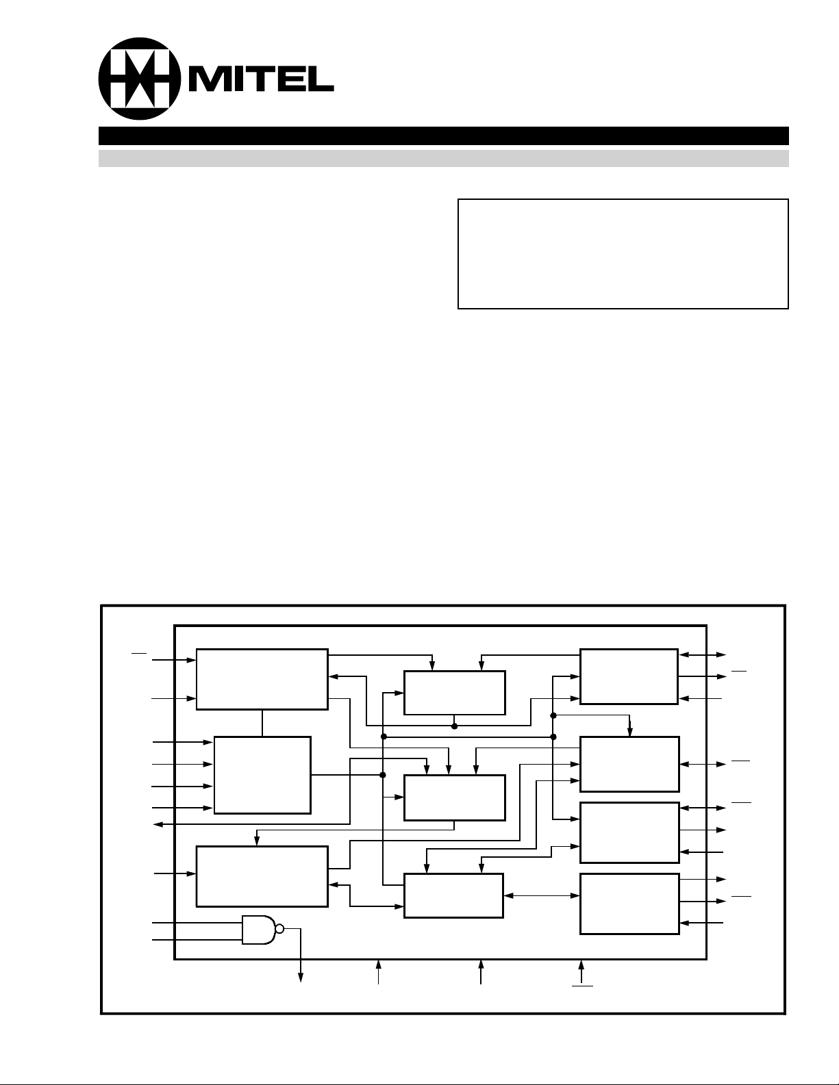
The MT8941 is a dual digital phase-locked loop
providing the timing and synchronization signals for
the T1 or CEPT transmission links and the ST-BUS.
The first PLL provides the T1 clock (1.544 MHz)
synchronized to the input frame pulse at 8 kHz. The
timing sign a l s fo r the CEPT transmi ss i on l i nk and th e
ST-BUS are provided by the second PLL locked to
an internal or an external 8 kHz frame pulse signal.
The MT8941 offers improved jitter performance over
the MT8940.
functional differences, which are listed in the section
on “Differences between MT8941 and MT8940”.
The two devices also have some
F0i
C12i
MS0
MS1
MS2
MS3
C8Kb
C16i
DPLL #1
2:1 MUX
Mode
Selection
Logic
DPLL #2
Ai
Bi
Yo V
DD
Input
Selector
Clock
Generator
V
SS
RST
Variable
Clock
Control
Frame Pulse
Control
4.096 MHz
Clock
Control
2.048 MHz
Clock
Control
CVb
CV
ENCV
F0b
C4b
C4o
ENC4o
C2o
C2o
ENC2o
Figure 1 - Functional Block Diagram
3-43
Page 2
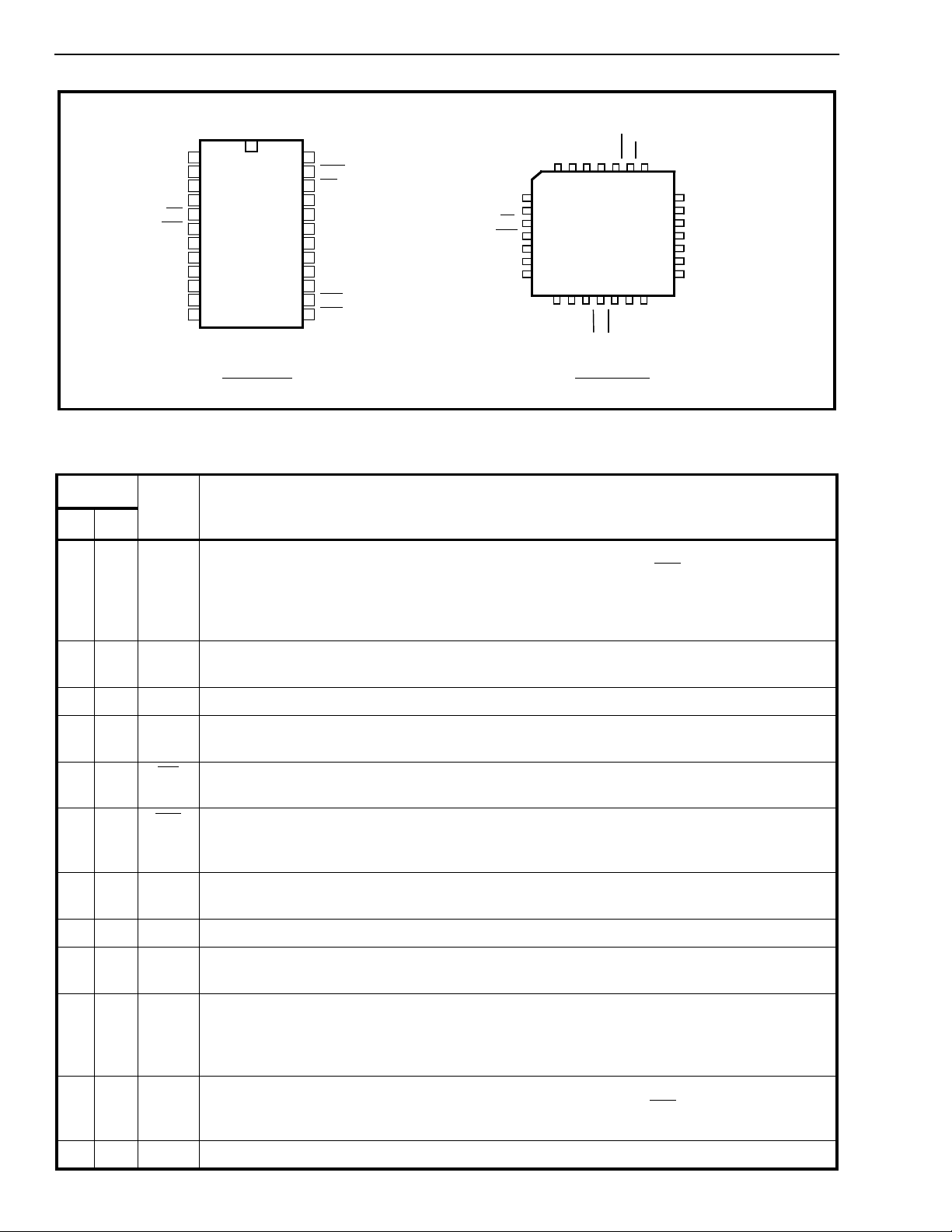
MT8941 CMOS
F0i
F0b
1
2
3
4
5
6
7
8
9
10
11
12
ENVC
MS0
C12i
MS1
MS2
C16i
ENC4o
C8Kb
C4o
VSS
Pin Description
24
23
22
21
20
19
18
17
16
15
14
13
VDD
RST
CV
CVb
Yo
Bi
Ai
MS3
ENC2o
C2o
C2o
C4b
Figure 2 - Pin Connections
NC
MS1
F0
F0b
MS2
C16i
ENC4o
V
i
0
C
D
2
C
1
N
C
4
3
5
6
i
7
8
9
10
11
2
3
1
1
o
b
4
K
8
C
C
28 PIN PLCC24 PIN PDIP
T
S
M
2
•
4
1
S
S
V
V
S
N
D
C
E
R
V
1
8
7
6
2
2
2
NC
25
CVb
24
Yo
23
22
Bi
21
Ai
20
MS3
19
5
7
6
1
1
1
b
o
o
4
2
2
C
C
C
ENC2o
8
1
C
N
Pin #
Name Description
DIP PLCC
11ENCVVariable clock enable (TTL compatible input) - This input directly controls the three states
of CV (pin 22) under all modes of operation. When HIGH, enables CV
and when LOW, puts
it in high impedance condition. It also controls the three states of CV b signal (pin 21) if MS1
is LOW. When ENCV is HIGH, the pin CVb is an output and when LOW, it is in high
impedance state. However, if MS1 is HIGH, CVb is always an input.
22MS0Mode sel ect ‘0’ input (TTL compatible) - This input in conjunction with MS1 (pin 4) selects
the major mode of operati on for bot h DPLLs. (Refer to Tabl es 1 and 2.)
33C12i12.352 MHz Clock input (TTL com pa tible) - Master clock input for DPLL #1.
46MS1Mode select-1 input (TTL compatible) - This input in conjunction with MS0 (pin 2) selects
the major mode of operati on for bot h DPLLs. (Refer to Tabl es 1 and 2.)
57 F0i
Frame pu lse inp ut (TTL com pati ble) - This is the frame pulse input at 8 kHz. DPLL #1
locks to the falling edge of this input to generate T1 (1.544 MHz) cloc k.
68F0b
Frame pu lse Bi directi on al (TT L comp atib le inp ut and Totem-pole outp ut) - Depending
on the minor mode selected for DPLL #2, it provides the 8 kHz frame pulse output or acts as
an input to an external frame pulse.
79MS2Mode se l ec t -2 input (TTL compatible) - This input in conjunction with MS3 (pin 17) selects
the minor mode of operati on for DP LL #2. (Refer to Table 3.)
810C16i16.384 MHz Clock input (TTL compa tibl e) - Master clock input for DPLL #2.
911EN
Enable 4.096 MHz clock (TTL comp atib le input) - This active high input enables C4o (pin
C4o
11) output. When LOW, the output C4o is in high impedance condition .
10 12 C8K b Clock 8 kHz Bidirectional (TTL com pati ble input and Totem-pole output) - This is the 8
kHz input signal on the falling edge of which the DPLL #2 locks during its NORMAL mo de.
When DPLL #2 is in SINGLE CLO CK mode, this pin output s an 8 kHz internal signal
provided by DPLL #1 which is also connected internally to DPLL #2.
11 13 C4o Clock 4.096 MH z (Three state outp ut) - This is the inverse of the signal appearing on pin
13 (C4b) at 4.096 MHz and has a rising edge in the frame pulse (F0b
) window. The high
impedance state of this out put is cont rolled by ENC 4o (pi n 9).
12 14 V
3-44
Ground (0 Volt)
SS
Page 3
Pin Description (continued)
CMOS MT8941
Pin #
Name Description
DIP PLCC
13 15 C4b Clock 4.096 M Hz - Bidirecti ona l (TTL comp atib le inpu t and Totem-pole outpu t) - When
the mode select bit MS3 (pin 17) is HIGH, it provides the 4.096 MHz clock output with the
falling edge in the frame pulse (F0b
) window. When pin 17 is LOW, C4b is an input to an
external clock at 4.096 MHz.
14 16 C2o
15 17 C2o Clock 2.048 MHz (Three state output) - This is the divide by two output of C4b
16 19 EN
Clock 2.048 MHz (Three state output) - This is the divide by two output of C4b (pin 13) and
has a falling edge in the frame pulse (F0b
is controlled by EN
C2o
(pin 16).
) window. The high impedance state of this output
(pin 13) and
has a rising edge in the frame pulse (F0b
controlled by EN
Enable 2.048 MHz clock (TTL compatible input) - This active high inp ut enables both C2o
C2o
C2o
(pin 16).
) window. The high impedance state of this output is
and C2o outputs (pins 14 and 15). When LOW, these outputs are in high impedance
condition.
17 20 MS3 Mode select 3 inpu t (TTL com pati ble) - This input in conjunction with MS2 (pin 7) selects
the minor mode of operation for DP LL #2. (Ref er to Table 3.)
18,1921,22Ai, Bi Inputs A and B (TTL compa tib le) -These are the two inputs of the uncomm itted NAND
gate
.
20 23 Y
Output Y (Totem pole output) - Output of the uncommitted NAND gate.
o
21 24 CVb Variable clock Bidirecti on al (TTL comp atib l e input and Totem-pole output) - When
acting as an output (MS1-LOW) during the NORMAL mode of DPLL #1, this pin provides the
1.544 MHz clock locked to the input frame pulse F0i
(pin 5). When MS1 is HIGH, it is an
input to an external clock at 1.544 MHz or 2.048 MHz to provide the internal signal at 8 kHz
to DPLL #2.
22 26 CV
23 27 RST
24 28 V
4,
DDVDD
NC No Connection.
5,
18,
25
Variable clock (Three state output) - This is the inverse output of the signal appearing on
pin 21, the high impedance state of which is control led by EN
CV
(pin 1).
Reset (S chmitt trigger input) - This input (active LOW) puts the MT8941 in its reset state.
To guarantee proper operation , the device must be reset afte r power-up. The time constant
for a power-up reset circuit (see Figures 9-13) must be a minimum of five times the rise time
of the power supply. In normal operation , the RST
pin must be held low for a minimum of
60nsec to reset the device.
(+5V) Power supply .
3-45
Page 4
MT8941 CMOS
Functional Description
The MT8941 is a dual digital phase-locked loop
providing the timing and synchronization signals to
the interface circuits for T1 and CEPT (30+2)
Primary Multiplex Digital Transmission links. As
shown in the functional block diagram (see Figure 1),
the MT8941 has two digital phase-locked loops
(DPLLs), associated output controls and the mode
selection logic circuits. The two DPLLs, although
similar in principle, operate independently to provide
T1 (1.544 MHz) and CEPT (2.048 MHz) transmission
clocks and ST-BUS timing signals.
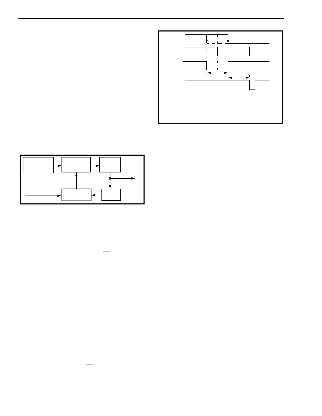
The principle of operation behind the two DPLLs is
shown in Figure 3. A master clock is divided down to
8 kHz where it is compared with the 8 kHz input, and
depending on the output of the phase comparison,
the master clock frequency is corrected.
Master clock
(12.352 MHz /
16.384 MHz)
Input (8 kHz)
The MT8941 achieves the frequency correction in
both directions by using three methods; speed-up,
slow-down and no-correction.
As shown in Figure 4, the falling edge of the 8 kHz
input signal (C8Kb for DPLL #2 or F0i
is used to sample the internally generated 8 kHz
clock and the correction signal (CS) once in every
frame (125 µs). If the sampled CS is “1”, then the
DPLL makes a speed-up or slow-down correction
depending upon the sampled value of the internal 8
kHz signal. A sampled ”0” or “1” causes the
frequency correction circuit to respectively stretch or
shrink the master clock by half a period at one
instant in the frame. If the sampled CS is “0”, then
the DPLL makes no correction on the master clock
input. Note that since the internal 8 kHz signal and
the CS signal are derived from the master clock, a
correction will cause both clocks to stretch or shrink
simultaneously by an amount equal to half the period
of the master clock.
Once in synchronization, the falling edge of the
reference signal (C8Kb or F0i) will be aligned with
either the falling or the rising edge of CS. It is aligned
with the rising edge of CS when the reference signal
is slower than the int ernal 8 kHz signal. On the other
hand, the falling edge of the
Frequency
Correction
Phase
Comparison
÷ 8
÷ 193 /
÷ 256
Figure 3 - DPLL Principle
for DPLL # 1)
Output
(1.544 MHz /
2.048 MHz)
C8Kb (DPLL #2)
(DPLL #1)
or F0i
l
Interna
8 kHz
correction
CS
F0b
(DPLL #2)
DPLL #1:
DPLL #2:
where, T
for DPLL #1 and T
for DPLL #2.
speed-up
region
t
= 4 × T
CS
tCS = 512 × T
t
CSF
is the 12.352 MHz master clock oscillator period
P12
t
CS
no-correction
± 0.5 × T
P12
± 0.5 × T
= 766 × T
P16
P16
is the 16.384 MHz master clock period
P16
sampling edge
correction
t
CSF
P12
P16
slow-down
region
Figure 4 - Phas e Com par ison
reference signal will be aligned with the falling edge
of CS if the reference signal is faster than the
internal 8 kHz signal.
Input-to-Ou tput Ph ase Re lationsh ip
The no-correction window size is 324 ns for DPLL #1
and 32 µs for DPLL #2. It is possib le for the relative
phase of the reference signal to swing inside the nocorrection window depending on its jitter and the
relative drift of the master clock. As a result, the
phase relationship between the input signal and the
output clocks (and frame pulse in case of DPLL #2)
may vary up to a maximum of window size. This
situation is illustrated in Figure 4. The maximum
phase variation for DPLL #1 is 324 ns and for DPLL
#2 it is 32µs. However, this phase difference can be
absorbed by the input jitter buffer of Mitel’s T1/CEPT
devices.
The no-correction window acts as a filter for low
frequency jitter and wander s ince the DPLL does not
track the reference signal inside it. The size of the
no-correction window is less than or equal to the size
of the input jitter buffer on the T1 and CEPT devices
to guarantee that no slip will occur in the received
T1/CEPT fra m e .
The circuit will remain in synchronization as long as
the input frequency is wit hin the lock-in range of the
DPLLs (refer to the section on “Jitter Performance
and Lock-in Range” for further details). The lock-in
range is wide enough to meet the CCITT line rate
specification (1.544 MHz ±32 ppm and 2.048 MHz
±50 ppm) for the High Capacity Terrestrial Digital
Service.
The phase sampling is done once in a frame (8 kHz)
for each DPLL. The divisions are set at 8 and 193 for
DPLL #1, which locks to the falling edge of the input
3-46
Page 5
CMOS MT8941
at 8 kHz to generate T1 (1.544 MHz) clock. For
DPLL #2, the divisions are set at 8 and 256 to
provide the CEPT/ST-BUS clock at 2.048 MHz
synchronized t o the falling edge of the input signal (8
kHz). The master clock source is specified to be
12.352 MHz for DPLL #1 and 16.384 MHz for DPLL
#2 over the entire temperature range of operation.
The inputs MS0 to MS3 are used to select the
operating mode of the MT8941, see Tables 1 to 4.
All the outputs are controlled to the high impedance
condition by their respective enable controls. The
uncommitted NAND gate is available for use in
applications involving Mitel’s M T8976/ MH89760 (T1
Interfaces) and MT8979/MH89790 (CEPT
Interfaces).
Modes of Operat ion
The operation of the MT8941 is categorized into
major modes and minor modes. The major modes
are defined for both DPLLs by the mode select pins
MS0 and MS1. The minor modes are selected by
pins MS2 and MS3 and are applicable only to DPLL
#2. There are no minor m odes for DPLL #1.
Major modes of DPLL #1
DPLL #1 can be operated in three major modes as
selected by MS0 and MS1 (Table 1). When MS1 is
LOW, it is in NORMAL mode, which provides a T1
(1.544 MHz) clock signal locked to the falling edge
of the input frame pulse F0i
requires a master clock input of 12.352 MHz (C12i).
In the second and third major modes (MS1 is HIGH),
DPLL #1 is set to DIVIDE an external 1.544 MHz or
2.048 MHz signal applied at CVb (pin 21). The
division can be set by MS0 to be either 193 (LOW) or
256 (HIGH). In these modes, the 8 kHz output at
C8Kb is connected internally to DPLL #2, which
operates in SINGLE CLOCK mode.
Major modes of DPLL #2
There are four major modes for DPLL #2 selectable
by MS0 and M S1, as s hown in Table 2. In all these
modes DPLL #2 provides the CEPT PCM30 timing,
and the ST-BUS clock and framing signals.
In NORMAL mode, DPLL #2 provides the CEPT/STBUS compatible timing signals loc ked to the falling
edge of the 8 kHz input signal (C8Kb). These
signals are 4.096 MHz (C4o and C4b
MHz (C2o and C2o
pulse (F0b
) derived from the 16.384 MHz master
) clocks, and the 8 kHz frame
clock. This mode can be the same as the FREERUN mode if the C8Kb pin is tied to V
(8 kHz). DPLL #1
) and 2.048
or VSS.
DD
M
M
S
1
Mode of
Operation
Provides the T1 (1.544 MHz) clock
synchronized to the falling edge of
the input frame pulse (F0i).
DPLL #1 divides the CVb input by
193. The divided output is
connected to DPLL #2.
DPLL #1 divides the CVb input by
256. The divided output is
connected to DPLL #2.
S
0
X 0 NORMAL
0 1 DIVIDE-1
1 1 DIVIDE-2
Note: X: indicates don’t care
Function
Table 1. Major Modes of DPLL # 1
M
M
S
1
Mode of
Operation
SINGLE
CLOCK-1
SINGLE
CLOCK-2
S
0
0 0 NORMAL
1 0 FREE-RUN
01
11
Provides CEPT/ST-BUS timing
signals locked to the falling edge of
the 8 kHz input signal at C8Kb.
Provides CEPT/ST-BUS timing and
framing signals with no external
inputs, except the master clock.
Provides CEPT/ST-BUS timing
signals locked to the falling edge of
the 8 kHz internal signal provided by
DPLL #1.
Provides CEPT/ST-BUS timing
signals locked to the falling edge of
the 8 kHz internal signal provided by
DPLL #1.
Function
Table 2. M ajor M odes of DP LL #2
M
M
S
S
2
3
11
01
00
10
Provides CEPT/ST-BUS 4.096 MHz and 2.048
MHz clocks and 8kHz frame pulse dependi n g on
the major mode selected.
Provides CEPT/ST-BUS 4.096 MHz & 2.048 MHz
clocks depending on the major mode selected
while F0b
F0b
has no effect on the operation of DPLL #2
unless it is in FREE-RUN mode.
Overrides the major mode selected and accepts
properly phase related external 4.096 MHz clock
and 8 kHz frame pulse to provide the ST-BUS
compatible clock at 2.048 MHz.
Overrides the major mode selected a nd acc epts a
4.096 MHz external clock to provide the ST-BUS
clock and frame pulse at 2.048 MHz and 8 kHz,
respectively.
Functional Description
acts as an input. However, the input on
Table 3. Minor Modes of DPLL #2
In FREE-RUN mode, DPLL #2 generates the standalone CEPT and ST-BUS timing and framing signals
with no external inputs except the master clock set at
16.384 MHz. The DPLL makes no correction in this
configurat ion and provides the t iming signals without
any jitte r.
3-47
Page 6
MT8941 CMOS
The operation of DPLL #2 in SINGLE CLOCK-1
mode is identical to SINGLE CLOCK-2 mode,
providing the CEPT and ST-BUS compatible timing
signals synchro-nized to the internal 8 kHz signal
obtained from DPLL#1 in DIVIDE mode. When
10) and DPLL #2 locks to the falling edge to provide
the CEPT and ST-BUS compatible timing signals.
This is in contrast to the Normal mode where these
timing signals are synchronized with the fallin g edge
of the 8 kHz signal on C8Kb.
SINGLE CLOCK-1 mode is selected for DPLL #2, it
automatically selects the DIVIDE-1 mode for DPLL
#1, and thus, an external 1.544 MHz clock signal
Minor modes of DPLL #2
applied at CVb (pin 21) is divided by DPLL #1 to
generate the internal signal at 8 kHz on to which
DPLL #2 locks. Similarly when SINGLE CLOCK-2
mode is selected, DPLL #1 is in DIVIDE-2 mode,
The minor modes for DPLL #2 depends upon the
status of the mode select bits MS2 and MS3 (pins 7
and 17).
with an external signal of 2.048 MHz providing the
internal 8 kHz signal to DPLL #2. In both these
modes, this internal signal is available on C8Kb (pin
M
M
M
Mode
S
#
0 0000
1 0 0 0 1 NORMAL MODE
2 0010
3 0011
4 0 1 0 0 DIVIDE-1 MODE Same as mode ‘0’.
5 0 1 0 1 DIVIDE-1 MODE
6 0 1 1 0 DIVIDE-1 MODE Same as mode 2.
7 0111
8 1 0 0 0 NORMAL MODE Same as mode ‘0’.
9 1001
10 1 0 1 0 NORMAL MODE Same as mode 2.
11 1011
12 1 1 0 0 DIVIDE-2 MODE Same as mode ‘0’.
13 1101
14 1 1 1 0 DIVIDE-2 MODE Same as mode 2.
15 1111
S
0
1
M
S
S
2
3
NORMAL MODE:
Provides the T1 (1.544 MHz) clock
synchronized to the falling edge of the input
frame pulse (F0i
NORMAL MODE
NORMAL MODE NORMAL MODE:
DIVIDE-1 MODE:
Divides the CVb input by 193. The divided
output is connected to DPLL #2.
NORMAL MODE F0b
NORMAL MODE
DIVIDE-2 MODE SINGLE CLOCK-2 MODE:
DIVIDE-2 MODE:
Divides the CVb input by 256. The divided
output is connected to DPLL# 2.
DPLL #1 DPLL #2
).
Operating Modes
Properly phase related External 4.096 MHz
clock and 8 kHz frame pulse provide the STBUS clock at 2.048 MHz.
NORMAL MODE:
is an input but has no function in this mode.
F0b
External 4.096 MHz provides the ST-BUS clock
and Frame Pulse at 2.048 MHz and 8 kHz,
respectively.
Provides the CEPT/ST-BUS compatible timing
signals locked to t h e 8 kHz input signal (C8Kb).
SINGLE CLOCK-1 MODE
F0b
is an input but has no function in this mode.
SINGLE CLOCK-1 MODE:
Provides the CEPT/ST-BUS compatible timing
signals locked to the 8 kHz internal signal
provided by DPLL #1.
is an input and DPLL #2 locks on to
it only if it is at 16 kHz to provide the ST-BUS
control signals.
FREE-RUN MODE:
Provides the ST-BUS timing signals with no
external inputs except the master clock.
F0b
is an input but has no function in this mode.
SINGLE CLOCK-2 MODE:
Provides the CEPT/ST-BUS compatible timing
signals locked to the 8 kHz internal signal
provided by DPLL #1.
Table 4. Sum mary o f Mo des o f Op eratio n - DP LL #1 and #2
3-48
Page 7
CMOS MT8941
When MS3 is HIGH, DPLL #2 operates in any of the
major modes selected by MS 0 and MS1. When MS3
is LOW, it overrides the major mode selected and
DPLL#2 accepts an external clock of 4.096 MHz on
(pin 13) to provide the 2.048 MHz clocks (C2o
C4b
and C2o
) and the 8 kHz frame pulse (F0b)
compatible with the S T-BUS format. The m ode select
bit MS2 controls the direction of the signal on F0b
(pin 6).
When MS2 is LOW, the F0b
pin is an 8 kHz frame
pulse input. This input is effective only when MS3 is
also LOW and pin C4b
is fed by a 4.096 MHz clock,
which has a proper phase relationship with the
signal on F0b
on pin F0b
(refer Figure 18). Otherwise, the input
will have no bearing on the operation of
DPLL #2, unless it is in FREE-RUN mode as
selected by MS0 and MS1. In FREE-RUN mode,
the input on F0b
is treated the same way as the
C8Kb input is in NORMAL mode. The frequency of
the signal on F0b
should be 16 kHz for DPLL #2 to
lock and generate the ST-BUS compatible clocks at
4.096 MHz and 2.048 MHz.
When MS2 is HIGH , the F0b
pin provides the frame
pulse output compatible with the ST-B US format and
locked to the internal or external input signal as
determined by the other mode select pins.
Table 4 summarizes the modes of the two DPLL. It
should be noted that each of the major modes
selected for DPLL #2 can have any of the minor
modes, although some of the combinations are
Mode
#
0 i:8 i:4.096 i:X o:1.544
1 i :X o:4.096 i:8 o:1.544
2 o:8 i:4.096 i:X o:1.544
3 o:8 o:4.096 i:8 o:1.544
4 i:8 i:4.096 i:X i:1.544
5 i :X o:4.096 o:8 i:1.544
6 o:8 i:4.096 i:X i:1.544
7 o:8 o:4.096 o:8 i:1.544
8 i:8 i:4.096 i:X o:1.544
9 i:16 o:4.096 i:X o:1.544
10 o:8 i:4.096 i:X o:1.544
11 o:8 o:4.096 i:X o:1.544
12 i:8 i:4.096 i:X i:2.408
13 i :X o:4.096 o:8 i:2.408
14 o:8 i:4.096 i:X i:2.408
15 o:8 o:4.096 o:8 i:2.408
F0b
(kHz)
C4b
(MHz)
C8Kb
(kHz)
CVb
(MHz)
Table 5. Functions of the Bidirectional Signals
in Each Mode
Notes: i : Input
o : Outp ut
X : “don’ t c are ” i np ut. Connect to V
DD
or V
SS.
functionally similar. The required operation of both
DPLL #1 and DPLL #2 must be considered when
determining MS0-MS3.
The direction and frequency of each of the
bidirectional s ignals are listed in Table 5 for each of
the given m odes in Table 4.
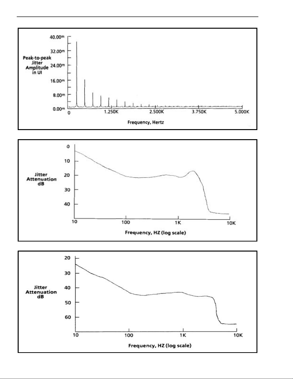
Jitter Performance and Loc k-in Range
The output jitter of a DPLL is composed of the
intrinsic jitter, measured when no jitter is present at
the input, and the output jitter resulting from jitter on
the input signal. The spectrum of the intr insic jitter
for both DPLLs of the MT8941 is shown in Figure 5.
The typical peak-to-peak value for this jitter is
0.07UI. The transfer function, which is the ratio of
the output jitter to the input jitter (both measured at a
particular frequency), is shown in Figure 6 for DPLL
#1 and Figure 7 for DPLL #2. The transfer function
is measured when the peak-to-peak amplitude of the
sinusoidal i n p ut ji tte r c o nf or ms to the fol low i n g :
10 Hz - 100 Hz : 13.6 µs
100 Hz - 10 kHz : 20 dB / decade roll-off
> 10 kHz : 97.2 ns
The ability of a DPLL to phase-lock the input signal
to the reference signal and to remain locked
depends upon its lock-in range. The lock-in range of
the DPLL is specified in terms of the maximum
frequency variation in the 8 kHz reference signal. It
is also directly affected by the oscillator frequency
tolerance. Table 6 lists different values for the lock-in
range and the corresponding oscillator frequency
tolerance for DPLL #1 and DPLL #2. The smaller
the tolerance value, the larger the lock-in range.
The T1 and CEPT standards specify that, for free
running equipment, the output clock tolerance must
be less than or equal to ±32ppm and ±50ppm
respectively. This require ment restr i cts the
Oscillator Clock*
Tolerance (±ppm)
5 2.55 1.91
10 2.51 1.87
20 2.43 1.79
32 2.33 1.69
50 2.19 1.55
100 1.79 1.15
150 1.39 .75
175 1.19 .55
Table 6. Lock -in Range vs. Osci llator Frequenc y
* Please refer to the section on “Jitter Performance and Lock-in
Range” for recommended oscillator tolerances for DPLL #1 & #2.
Lock-in Range (±Hz)
DPLL #1 DPLL #2
Tolerance
3-49
Page 8
MT8941 CMOS
Fig. 5- The Spectrum of the Inherent Jitter for either PLL
3-50
Fig. 6 - The Ji tter Transfer Fu nction for PL L1
Fig. 7 - The Ji tter Transfer Fu nction for PL L2
Page 9

CMOS MT8941
oscillators of DPLL #1 and DPLL #2 to have
maximum tolerances of ±32ppm and ±50ppm
respectively.
However, if DPLL #1 and DPLL #2 are daisy-chained
as shown in Figures 9 and 10, the output clock
tolerance of DPLL #1 will be equal to that of the
DPLL #2 oscillator when DPLL #2 is free-running. In
this case, the oscillator tolerance of DPLL #1 has no
impact on its output clock tolerance. For this reason,
a) Distributed Timing
Data Bus
8 kHz Reference Signal
M
U
X
it is recommended to use a ±32 ppm oscillator for
DPLL #2 and a ±100 ppm oscillator for DPLL #1.
Differences betwe en MT8941 and MT8940
The MT8941 and MT8940 are pin and mode
compatible for most applications. However, the user
should take note of the following differences between
the two parts.
Line Card 1
MT8940
Clocks
8 kHz Reference Signal
b) Centralized Timing
8 kHz Reference Signal
M
U
X
MT8941
Clocks
Data Bus
MT8940
Line Card n
Clocks
Line Card 1
Line Card n
8 kHz Reference Signal
Figure 8 - Application Differences between the MT8940 and MT8941
3-51
Page 10

MT8941 CMOS
Besides the improved jitter performance, the
MT8941 differs from the MT8940 in three other
areas:
1. Input pins on the MT8941 do not incorporate
internal pull-up or pull-down resistors. In
addition, the output configuration of the
bidirectional C8Kb pin has been converted from
an open drain output to a Totem-pole output.
2. The MT8941 includes a no-correction window to
filter out low frequency jitter and wander as
illustrated in Figure 4. Consequently, there is no
constant phase relationship between reference
signal F0i
of DPLL # 1 or C8Kb of DPLL #2 and
the output clocks of DPLL #1 or DPLL #2.
Figure 4 shows the new phase relationship
between C8Kb and the DPLL #2 output clocks.
Figure 8 illustrates an application where the
MT8941 cannot replace the MT8940 and
suggests an alternat ive solution.
3. The MT8941 must be reset after power-up in
order to guarantee proper operation, which is not
the case for the MT8940.
4. For the MT8941, DPLL #2 locks to the falling
edge of the C8Kb reference signal. DPLL#2 of
the MT8940 locks on to the rising edge of C8Kb.
5. While the MT8940 is available only in a 24 pin
plastic DIP, the MT8941 has an additional 28 pin
PLCC package option.
Applications
The following figures illust rates how the MT8941 can
be used in a minim um component count approach in
providing the timing and synchro-nization signals for
the Mitel T1 or CEPT interfaces, and the ST-BUS.
The hardware selectable modes and the
independent control over each PLL adds flexibility to
the interface circuits. It can be easily reconfigured to
provide the timing and control signals for both the
master and slave ends of the link.
Synchronization and Timing Signals for the T1
Transmission L ink
Figures 9 and 10 show examples of how to generate
the timing signals for the master and slave ends of a
T1 link. At the master end of the link (Figure 9),
DPLL #2 is the source of the S T-BUS signals deriv ed
from the crystal clock. The frame pulse output is
looped back to DPLL #1 (in NORMAL mode), which
locks to it to generate the T1 line clock. The timing
relationship between the 1.544 MHz T1 clock and
the 2.048 MHz ST-BUS clock meets the
requirements of the MH89760/760B. The crystal
clock at 12.352 MHz is used by DPLL #1 to generate
the 1.544 MHz clock, while DPLL #2 (in FREE-RUN
mode) uses the 16.384 MHz crystal oscillator to
generate the ST-BUS clocks for system timing. The
generated ST-BUS signals can be used to
synchronize the system and the switching equipment
at the master end.
Crystal Clock
(12.352 MHz)
Crystal Cloc k
(16.384 MHz)
3-52
MT8980/81
ST-BUS
SWITCH
(1.544 Mbps)
MS0
MS1
MS2
MS3
F0i
C12i
EN
CV
C8Kb
C16i
EN
C4o
EN
C2o
V
SS
MT8941
C
RST
V
DD
CVb
C4b
C2o
F0b
MH89760B
C1.5i
C2i
F0i
V
DD
R
DPLL #1 - NORMAL (MS0 = X; MS1 = 0)
DPLL #2 - FREE-RUN (MS0=1; MS2=1; MS3=1)
DSTi
DSTo
CSTi
CSTo
TxT
TRANSMIT
TxR
RxT
RxR
Mode of Operation for the MT8941
RECEIVE
Figure 9 - Synchronization at the Master End of the T1 Transmission Link
T1
LINK
Page 11

CMOS MT8941
Crystal Clock
(12.352 MHz)
Crystal Clock
(16.384 MHz)
Crystal Clock
(16.384 MHz)
MT8980/81
SWITCH
(1.544 Mbps)
MS0
MS1
MS2
MS3
F0i
C12i
EN
CV
C8Kb
C16i
EN
C4o
EN
C2o
V
SS
MT8941
C
RST
V
DD
CVb
C4b
C2o
F0b
MH89760B
C1.5i
C2i
F0i
E8Ko
R
V
DD
DPLL #1 - NORMAL ( MS1=0)
DPLL #2 - NORMAL (MS0=0; MS1=0; MS2=1; MS3=1)
DSTi
DSTo
CSTi
CSTo
TxT
TxR
RxT
RxR
Mode of Operation for the MT8941
TRANSMIT
RECEIVE
Figure 10 - Synchronization at the Slave End of the T1 Transmission Link
MS0
MS1
MS2
MS3
F0i
C12i
EN
CV
C8Kb
C16i
EN
C4o
EN
C2o
V
SS
MT8941
RST
V
DD
C4b
C2o
F0b
Y
MH89790B
DSTi
C2i
F0i
o
DSTo
CSTi0
CSTi1
CSTo
OUTA
OUTB
RxT
RxR
TRANSMIT
RECEIVE
MT8980/81
ST-BUS
SWITCH
CEPT
PRIMARY
MULTIPLEX
DIGITAL
ST-BUS
T1
LINK
LINK
V
DD
C
R
Figure 11 - Synchronization at the Master End of the CEPT Digital Transmission Link
At the slave end of the link (Figure 10) both the
DPLLs are in NORMAL mode, with DPLL #2
providing the ST-BUS timing signals locked to the 8
kHz frame pulse (E8Ko) extracted from the received
signal on the T1 line. The regenerat ed frame pulse
is looped back to DPLL #1 to provide the T1 line
clock, which is t he same as the master end.
The 12.352 MHz and 16.384 MHz crystal clock
sources are necessary for DPLL #1 and #2,
respectively.
Mode of Operation for the MT8941
DPLL #1 - NOT USED
DPLL #2 - FREE-RUN (MS0=1; MS1=0; MS2=1; MS3=1)
Synchronization and Timing Signals for the
CEPT Transmissi o n L i n k
The MT8941 can be used to provide the timing and
synchronization signals for the MH89790/790B,
Mitel’s CEPT (30+2) Digital Trunk Interface Hybrid.
Since the operational frequencies of the ST-BUS and
the CEPT primary multiplex digital trunk are the
same, only DPLL #2 is required.
3-53
Page 12

MT8941 CMOS
MT8941
V
DD
C4b
C2o
F0b
Y
o
V
DD
R
Crystal Cloc k
(16.384 MHz)
MS0
MS1
MS2
MS3
F0i
C12i
EN
CV
C8Kb
C16i
EN
C4o
EN
C2o
V
SS
RST
C
Figure 12 - Synchronization at the Slave End of the CEPT Digital Transmission Link
Figures 11 and 12 show how the MT8941 can be
used to synchronize the ST-BUS to the CEPT
transmission link at the master and slave ends.
Genera ti on o f S T-BUS Timi ng S ig nal s
The MT8941 can source the properly formatted STBUS timing and control signals with no external
inputs except the crystal clock. This can be used as
the standard timing source for ST-BUS systems or
any other system with similar clock requirements.
MT8980/81
MH89790B
DSTi
C2i
F0i
E8Ko
DPLL #1 - NOT USED
DPLL #2 - NORMAL (MS0=1; MS1=0; MS2=1; MS3=1)
DSTo
CSTi0
CSTi1
CSTo
OUTA
OUTB
RxT
RxR
Mode of Operation for the MT8941
TRANSMIT
RECEIVE
ST-BUS
SWITCH
CEPT
PRIMARY
MULTIPLEX
DIGITAL
LINK
Figure 13 shows two such applications using DPLL
#2. In one case, the MT8941 is in FREE-RUN
mode with an oscillator input of 16.384 MHz. In the
other case, it is in NORMAL mode with the C8Kb
input tied to V
. For these applications, DPLL #2
DD
does not make any corrections and therefore, the
output signals are free from jitter. DPLL #1 is
completel y free.
For prototyping purposes, Mitel offers the MT8941
Crystal Kit (MB6022) which contains 16.384 MHz
and 12.352 MHz clock oscillators.
Crystal Clock
(16.384 MHz)
3-54
DPLL #1 - NOT USED
DPLL #2 - FREE-RUN MODE
(MS0=0; MS1=0;MS2=1;
MS0
MS1
MS2
MS3
F0i
C12i
EN
CV
C8Kb
C16i
EN
C4o
EN
C2o
Ai
Bi
V
SS
MT8941
V
C4o
C4b
C2o
C2o
F0b
RST
C
DD
R
MS3=1)
ST-BUS
TIMING
SIGNALS
DPLL #1 - NOT USED
DPLL #2 - NORMAL MODE
(MS0=0; MS1=0;
MS2=1; MS3=1)
V
DD
Crystal Clock
(16.384 MHz)
Figure 13 - Generation of the ST-BUS Timing Signals
MS0
MS1
MS2
MS3
F0i
C12i
EN
CV
C8Kb
C16i
EN
C4o
EN
C2o
Ai
Bi
V
SS
MT8941
RST
C
V
C4o
C4b
C2o
C2o
F0b
DD
R
ST-BUS
TIMING
SIGNALS
V
DD
Page 13

CMOS MT8941
Absolute Maximum Ratings*- Voltages are with respect to ground (V
) unless otherwise stated.
SS
Parameter Symbol Min Max Units
1 Supply Voltage V
2 Voltage on any pin V
3 Input/Outp ut Diode Current I
4 Outpu t Source or Sink Current I
5 DC Supply or Ground Current I
6 Storage Temperature T
7 Package Power Dis sipatio n Plasti c DIP
PLCC
* Exceeding these values ma y cause perm an ent dama ge. Functi onal operati on under these cond ition s is not implied.
DD
I
IK/OK
O
DD/ISS
ST
P
D
P
D
Recommended Operating Conditions - Voltages are with respect to ground (V
Characteristics Sym M in Typ
1 Supply Voltage V
2 I nput HIGH Voltage V
3 Input LOW Voltage V
4 O perat ing Temperature T
‡ Typical figures are at 25°C and are for design aid only: not guaranteed and not subject to producti on testing.
DD
IH
IL
A
4.5 5.0 5.5 V
2.0 V
V
SS
-40 25 85
‡
Max Units Test Conditions
DD
0.8 V
-0.3 7.0 V
VSS-0.3 VDD+0.3 V
-55 125
) unless otherwise stated .
SS
V
o
C
±10 mA
±25 mA
±50 mA
o
1200
600
mW
mW
C
DC Electrical Characteristics - Voltages are with respect to gro un d (V
V
=5.0V±5%; VSS=0V; TA=-40 to 85°C.
DD
Characteristics Sym Min Typ‡Max Units Test Conditions
S
U
1
2
Supply Current
P
Input HIGH voltage (For all the
inputs except pin 23)
3 Positive-going threshold
voltage (For pin 23)
I
N
4 Input LOW voltage (For all the
inputs except pin 23)
5 Neg ati ve -going th re sh old
voltage (For pin 23)
O
6
7 Outp ut current LOW I
Output current HIGH I
U
T
8 Leakage cu rrent on bidirect-
ional pins and all inputs ex cept
C12i, C16i, RST
, MS1, MS0
I
V
V
V
DD
2.0 V
IH
+
IL
V
OH
OL
I
1.0 1.5 V
-
-4 mA VOH=2.4 V
4mAV
-100 -30 -8 µA
IL
815mA
3.0 4.0 V
) unless otherwise stated.
SS
Under clocked condition, with the
inputs tied to the same supply
rail as the corresponding pull-up
/down resistors.
0.8 V
VIN=VSS
OL
=0.4 V
9 Leakage cu rren t on pins MS1,
I
IL
10 35 120 µAVIN=V
MS0
10 Leakage current on all three-
I
-10 ±1 +10 µAV
IL
state outputs and C12i, C16i,
RST
inputs
‡ Typical figures are at 25°C and are for design aid only: not guaranteed and not subject to producti on testing.
DD
I/O=VSS
or V
DD
3-55
Page 14

MT8941 CMOS
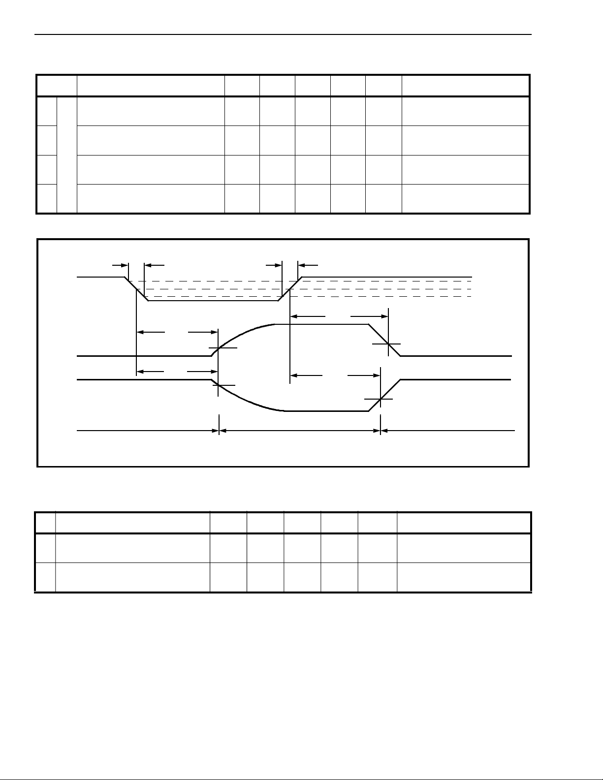
AC Electrical Characteristics†- Voltages are with respect to ground (V
Characteristics Sym Min Typ
1
2 CVb output (1.544 MHz) fall
3 CVb output (1.544 MHz) clock
4 CVb output (1.544 MHz) clock
5 CVb output (1.544 MHz) clock
6CV
7CV
† Timing is over recommended temperature & power supply voltages.
‡ Typical figures are at 25°C and are for design aid only: not guaranteed and not subject to producti on testing.
CVb output (1. 544 MHz) rise
time
time
D
P
period
L
L
width (HIGH)
#1
width (LOW)
delay (HIGH to LOW) t
delay (LOW to HIG H) t
t
r1.5
t
f1.5
t
P15
t
W15H
t
W15L
15HL
15LH
6ns
6 ns 85 pF Load
607 648 689 ns
318 324 ns
277 363 ns
010ns
-7 3 ns
) unless otherwise stated. (Refer to Figure 14)
SS
‡
Max Units Test Conditions
85 pF Load
t
P15
t
W15H
V
CVb
CV
OH
V
OL
t
15HL
V
OH
V
OL
t
15LH
Figur e 14 - Tim ing Info r mat io n fo r DP LL #1 in NO RM A L Mo de
AC Electrical Charac teristic s†- Voltages are with respect to ground (V
Characteristics Sym Min Typ
1
2 C8Kb output (8 kHz) delay
3 C8Kb out put duty cycle 66
C8Kb output (8kHz) delay
(HIGH to HIGH)
D
(LOW to LOW )
P
L
t
C8HH
t
C8LL
0 10 25 ns 85 pF Load
2 13 34 ns 85 pF Load
L
‡
50
t
f1.5
t
W15L
t
r1.5
) unless otherwise stated. (Refer to Figure 15)
SS
Max Units Test Conditions
%
In Divide -1 Mode
%
In Divide - 2 Mode
4 Inverted clock output delay
#1
(HIGH to LOW )
5 Inverted clock output delay
(LOW to HIGH)
† Timing is over recommended temperature & power supply voltages.
‡ Typical figures are at 25°C and are for design aid only: not guaranteed and not subject to producti on testing.
3-56
t
ICHL
t
ICLH
01025ns
0 7 18 ns
Page 15

CVb
CMOS MT8941
V
IH
V
IL
CV
C8Kb
F0b
C4b
t
ICHL
V
OH
V
OL
t
C8HH
V
OH
V
OL
t
ICLH
t
C8LL
Figure 15 - DPLL #1 in DIVIDE Mode
t
WFP
V
OH
V
OL
t
FPL
t
W4oH
V
OH
V
OL
t
W4oL
t
FPH
t
4oLH
t
4oHL
t
fC4
t
P4o
t
rC4
C4o
C2o
C2o
V
OH
V
OL
t
V
OH
V
OL
V
OH
V
OL
42HL
t
W2oL
t
42LH
t
W2oH
t
2oLH
t
P2o
t
t
fC2
rC2
t
2oHL
Figure 16 - Timing Information on DPLL #2 Outputs
3-57
Page 16

MT8941 CMOS
AC Electrical Characteristics
†
-Voltages are with respe ct to groun d (V
Characteristics Sym Min Typ
1
2C4b
3C4b
4C4b
5C4b
output clock period t
C4b
output clock width (HI G H) t
output clock width (LOW) t
output clock rise tim e t
clock output fall time t
6 Fram e pulse out put delay
(HIGH to LOW) from C4b
7 Fram e pulse out put delay
(LOW to HIGH) from C4b
8 Fram e pulse (F0b
D
9 C4o dela y - LOW to HIGH t
P
L
10 C4o dela y - HIGH to LOW t
L
11 C4b
#2
12 C4b
to C2o delay (LOW to
HIGH)
to C2o delay (HIGH to
) width t
LOW)
P4o
W4oH
W4oL
rC4
fC4
t
FPL
t
FPH
WFP
4oLH
4oHL
t
42LH
t
42HL
) unless otherwise stated.(Refer to Figure 16)
SS
‡
Max Units Test Conditions
213 244 2 75 ns 85 pF Load
85 159 ns
116 122 ns
6 ns 85 pF L oad
6 ns 85 pF L oad
013ns
08ns
85 pF Load
85 pF Load
225 245 ns
015ns
020ns
03ns
06ns
13 C2o clock period t
14 C2o clock width ( HIGH ) t
15 C2o clock width ( LOW ) t
16 C2o clock rise time t
17 C2o clock fall tim e t
18 C2o
19 C2o
† Timing is over recommended temperature & power supply voltages.
‡ Typical figures are at 25°C and are for design aid only: not guaranteed and not subject to producti on testing.
delay - LOW to HIGH t
delay - HIGH to LOW t
P2o
W2oH
W2oL
rC2
fC2
2oLH
2oHL
457 488 5 19 ns 85 pF Load
207 280 ns
238 244 ns
6 ns 85 pF L oad
6 ns 85 pF L oad
-5 2 ns
057ns
3-58
Page 17

CMOS MT8941
AC Electrical Characte rist ics† - Voltages are with respect to ground (V
Characteristi cs Sym Mi n Typ
1
Master clocks input rise time t
2 Master clocks input fall time t
3 Master clock period
C
(12.352MHz)*
L
O
4
Master clock period
C
(16.384MHz)*
K
S
5 Duty Cycle of master clocks 45 50 55 %
6 Lock-in Range DPLL #1
DPLL #2
† Timing is over recommended temperature & power supply voltages.
‡ Typical figures are at 25°C and are for design aid only: not guaranteed and not subject to producti on testing.
* Please revie w the sect ion on "Jitter Perfor ma nce and Lock-in Range".
t
r
Master clock
inputs
2.4 V
1.5 V
0.4 V
t
P12
t
P16
t
r
f
80.943 80.958 80.974 ns
61.023 61.035 61.046 ns
-2.33
-1.69
or t
P12
P16
‡
) unless otherwise stated. (Refer to Figure 14)
SS
Max Units Test Con ditio ns
10 ns
10 ns
For DPLL #1, while operating to
provide the T1 clock signal.
For DPLL #2, while operating to
provide the CEPT and ST-BUS
timing signals.
+2.33
+1.69
Hz
With the Master frequency
tol erance at ±32 ppm.
t
f
Figure 17 - Master Clock Inputs
AC Electrical Charact eristics
Characteristics Sym Min Typ
1F0b
2C4b
3 Frame pulse (F0b
4 Frame pulse (F0b
† Timing is over recommended temperature & power supply voltages.
‡ Typical figures are at 25°C and are for design aid only: not guaranteed and not subject to producti on testing.
F0b
C4b
input pulse width (LOW ) t
input clock period t
) setup time t
) hold time t
V
IH
V
IL
V
IH
V
IL
t
FS
†
Voltages are with respect to ground (V
‡
WFP
P4o
FS
FH
t
WFP
t
FH
244 ns
244 ns
50 ns
25 ns
t
P4o
) unless otherwise stated. (Refer to Figure 18)
SS
Max Units Test Conditions
Figure 18 - Ex terna l Inputs on C4b and F0b fo r the DPL L #2
3-59
Page 18
MT8941 CMOS
AC Electrical Characte rist ics
Characteristics Sym Min Typ
1
Delay from Enable to Outpu t
(HIGH to THREE STATE)
†
Voltages are with respect to ground (V
-
t
PHZ
) unless otherwise stated. (Refer to Figure 19)
SS
‡
Max Units Test Conditions
16 ns 85 pF Load
O
2 Delay from Ena ble to Outpu t
U
(LOW to THREE STATE)
T
P
3 Delay from Ena ble to Outpu t
U
(THREE STATE to HIGH)
t
PLZ
t
PZH
12 ns 85 pF Load
11 ns 85 pF Load
T
4 Delay from Ena ble to Outpu t
(THREE STATE to LOW)
† Timing is over recommended temperature & power supply voltages.
‡ Typical figures are at 25°C and are for design aid only: not guaranteed and not subject to producti on testing.
Enable
Input
Output
LOW to
OFF
Output
HIGH
to OFF
t
f
Outputs
Enabled
6 ns t
t
PLZ
t
PHZ
t
PZL
r
10%
90%
50 16 ns 85 pF Load
6 ns
t
PZL
t
PZH
1.3 V
Outputs
Disabled
1.3 V
Outputs
Enabled
3.0 V
2.7 V
1.3 V
0.3 V
Figure 19 - Three State Outputs and Enable Timings
AC Electrical Characteristics† - Uncommitted NAND Gate
Voltages are with respect to ground (VSS) unless otherwise stated.
Characteristics Sym Min Typ
1 Propagation delay (LOW to
HIGH), input Ai or Bi to output
2 Propagation delay (HIGH to
LOW), input Ai or Bi to output
† Timing is over recommended temperature & power supply voltages.
‡ Typical figures are at 25°C and are for design aid only: not guaranteed and not subject to producti on testing.
t
PLH
t
PHL
‡
Max Units Test Conditions
11 ns 85 pF Load
15 ns 85 pF Loa d
3-60
 Loading...