

Page 1
MT8924
PCM Conference Circuit (PCC)
Preliminary Information
Features
• Supports up to 10 indepen dent confere nces for
up to 32 PCM Voice Channels
• ST-BUS compatibl e 2.048 M b/s PCM Se rial
Interface (al so su pports 1.536 M b/s an d 1.5 44
Mb/s data rates)
• Per channel digita l gain contro l (0/-3/ -6 dB)
• Parallel microprocessor port for device control
• Programmab le noi se su ppres sion
• External Tone Input
• Pin select able A/µ -Law format
• Low power CM OS t echnol ogy
• Available in 24 P in PD IP an d SO IC pa ckage s
Applications
• Digital PBX / KTS
• Conference b rid ges
• Digit al C .O . s witc h es
ISSUE 1 April 1994
Ordering Information
MT8924AE 24 Pin Plastic DIP
MT8924A S 24 Pin SOIC
°
C to +70°C
0
Description
The MT8924 is designed to provide conference call
capability in digital switching systems. It allows up to
10 independent conferences to be set for up to 32
PCM voice channels.
A/µ-Law companded data from the PCM input port is
converted to linear format, processed by a dedicated
arithmetic unit, re-converted to companded format
and then sent to the PCM output port.The PCM
output signal contains all the information of each
channel connected in conference except its own.
Programmable attenuation and noise suppression
are provided for channels connected in conference
or transparent mode. Additionally, an input for an
external tone is featured that can be used as a signal
to indicate to connected parties that they are on a
conference call.
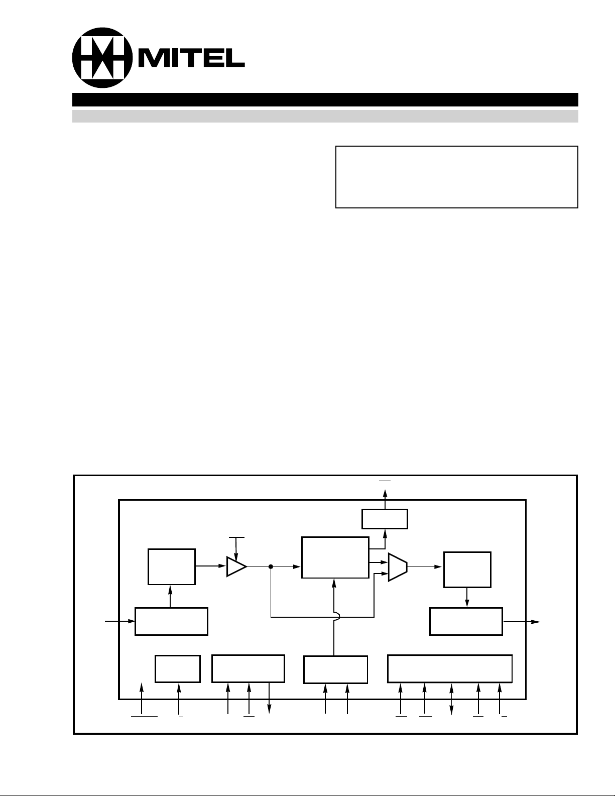
DSTi
OS
Overflow
Attenuation/Noise Suppression
Channel RAM
µ/A-Law
to
Linear
Serial-to -Parallel
Conversion
PCM Mode
Control
RESET WRRD CS C/ D
A/µ
Timebase
Cki F0i
Cko D0-D7TDTF
and
Adder
PCM Tone
Generator
Linear
MUX
to
µ/A-Law
Parallel-to-Serial
Conversion
Control
Figure 1 - Functional Block Diagram
DSTo
8-3
Page 2
MT8924 Preliminary Information
TD
TF
RESET
OS
DSTo
D7
D6
D5
D4
D3
D2
D1
10
11
12
1
2
3
4
5
6
7
8
9
24
23
22
21
20
19
18
17
16
15
14
13
VSS
A/µ
DSTi
Cko
Cki
F0i
WR
RD
CS
C/D
VDD
D0
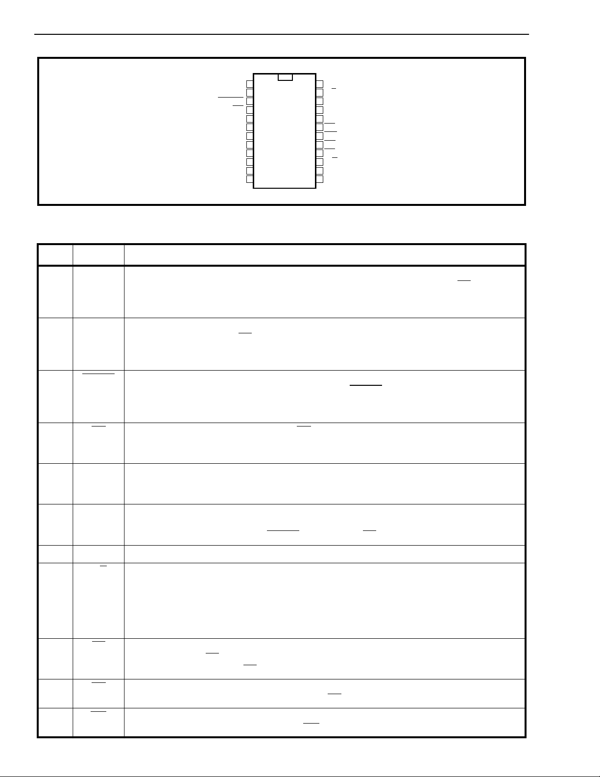
Figure 2 - Pin Connections
Pin Description
Pin # Name Description
1TDTone Duration (Input). When TD is High, a PCM-coded tone is sent out to all channels of
the enabled conferences instead of PCM dat a. TD is latched by frame pulse F0i
channels have the same tone during the same frame numb er. When TD is Low, normal
operation is enabled.
2TFTone Frequency (In put). This input is connected to an external squarewave generator. TF
is strobed by frame pulse F0i
so that all channels have the same tone frequency during the
same number of frames. Th e PCM-coded ton e level corresponds to 1/10th of the full scale
value, and is activated when TD is High.
so that all
3 RESET
Master RESET (Input). This input is used for system initializat ion after power up, or when
the companding law format has been changed. The RESET
pin is strobed by the rising edge
of clock Cki. Complete circuit initialization takes two frame periods. Initialization disables the
output drivers of the microprocessor interfa ce and DSTo.
4OS
Overflow Signalling (Output). When OS is Low, a conference is in the overflow condition.
This signal is delayed by half of a timeslot relative to the beginning of the output channe l of
the conference in overflow (se e Figure 9).
5DST
ST-BUS Seria l O u t p u t. This pin is the output for the PCM signal. It is enabled upon
o
channel selection, otherwise it is placed in a high impedance state. Maximu m bit rate is
2.048 Mb/s.
6-13 D7 to D0 Data Bus I/O Port. These are bidirectional data pins over which data and instructions are
transferred to and from the microprocessor (where D0 is the least significant bit). The bus is
14 V
DD
15 C/D
in a high impedance state when RESET
Positive Supply Voltage. Nominally 5 volts.
Control/Data Select (Input). The signal on this input defines whether the information on the
is Low and/or CS is High.
data bus should be interpreted as opcode or data. During a write operation a Low signal
defines the bus content as data, while a High signal def ines it as opcode. During a read
operatio n this input differen tiat es overflo w statu s between the first eig ht channels for C/D
being LOW, and the last two channels for C/D being HIGH (see Instruction 4). This input also
allows status monitoring (see Inst ructio n 6) during a read operation.
16 CS
Chip Select (Input). This active low input selects the device for microprocessor read/write
operations. When CS
microprocessor, and when CS
is Low, data and instructions can be transferred to or from the
is High, the data bus is in a high impedance state.
17 RD
18 WR
8-4
Read (Input). This active low input is for the read signal on the microprocessor interface.
The data bus is updated on the falling edge of RD
.
Write Input. This active low input is for the write signal on the microprocessor interface. The
data bus is strobed on the rising edge of WR
.
Page 3
Preliminary Information MT8924
Pin Description (continued)
Pin # Name Description
19 F0i Frame Pulse (Input). This is an 8 kHz active low input used for frame synchronization of the
PCM bit stream. The first falling edge of Cki followin g the falling edge of frame pulse F0i
determines the start of a new frame and mu st correspond to the first bit of the first channel.
When PCM frames o f 1544 kbit/s are used, the rising edge of F0i
must correspond to the
Extra (193rd) bit.
20 Cki Clock (Input). This signal is the timing reference used for all int ernal operat ion s. The PCM
bit cell boundaries lie on the alternate fall ing edges of this clock. The maxim um all owable
clock frequency is 4096 kHz.
21 Cko Clock (Output). This pin provides the master clock for a digital crosspo int switch (e.g. ,
MT898x series, or the MT9080, MT9085 co mbi nat ion). Normall y the signal on this pin is
identical to Cki. Wh en Extra bit operating m ode is selected (see Inst ructio n 5), the first two
cycles of the master clock are suppressed (see Figure 10). This feature allows the MT8924
to operate in 1544 kbit/s systems.
22 DST
ST-BUS Serial Input. This pin accepts the serial PCM input stream at a maximum allowable
i
bit rate of 2048 kbit/s. In normal operation the first bit of the first channel is defi ned by the
rising edge of Cki following the falling edge of fram e pulse F0i
mode is selected, the first bit of the first channel defines the extra bit.
23 A/µ
A/µ - Law Select Input. When A/µ is High, A-Law is selected, and when A/µ is Low, µ -Law is
selected. The companding law selection m ust be done before init iali zing the device using
pin.
24 V
the RESE T
Negative Power Supply Voltage. Nominally 0 Volts.
SS
Functional Description
The MT8924 is a device designed to provide
conferencing in a digital switching system in any
combination for up to all 32 channels of a 2048 kbit/s
ST-BUS stream (see Figure 3).
The information of channel N, frame M is first
converted to Linear PCM and then added to the
signal from other conferencees during the first half of
Microcontroller
STi0
.
.
.
.
STix-1
STix
MT8980/81/82
Digital Switch
MT8924
PCM Conference
Circuit (PCC)
STo0
.
.
.
.
STox-1
STox
. When Extra bit opera tin g
channel N+1, frame M and subtracted during the
second half of channel N-1, frame M+1. After Linearto-PCM conversion the subtraction result goes to the
parallel-to-serial converter, and appears at the
output on the N+1 channel, M+1 frame with respect
to the corresponding sending party information (see
Figure 4).
To a microprocessor the MT8924 appears as a
memory mapped peripheral device that can be
controlled by a set of six instructions. These
commands can be used to establish or cancel
conferences between the PCM channels and also to
transmit control messages on specific operating
modes. The microprocessor can initiate and receive
status messages or check conference connections
that are currently in operation.
Output
Information
B+C A+C A+B
DSTo
N+2 N+3N+1
Output Channels
Frame M+1
DSTi
Input
Information
B
A
Input Channels
Frame M
C
N+2N+1N
MT8924
Figure 3 -Typical Conference Connec tion
Figure 4 - Input/ Outp ut Chan nel Relati on shi p
8-5
Page 4
MT8924 Preliminary Information
Noise
Threshold
A-Law 1/4096 1000 0000 0000 0000
9/4096 1000 0100 0000 0100
16/4096 1000 1000 0 000 1000
32/4096 1000 1111 0000 1111
µ-Law 1 /8159 1111 1111 011 1 11 11
9/8159 1111 1011 0111 1011
16/8159 1111 0111 0111 0111
32/8159 1111 0000 0111 0000
Table 1 - PCM Noise Suppression Threshold Levels
Overflow Detection / Input Channel Attenuation
If the sum of the channels involved in one
conference exceeds the full scale value of the
accumulator, an overflow condition is generated
which can be monitored specifically by reading the
status of the overflow register. If an overflow
condition occurs, then each channel in a conference
can be independently attenuated if desired.
PCM Byt e
+ve input -ve input
B7 - B0 B7 - B0
Alternatively, a conference in the overflow condition
can be detected using the OS
with frame pulse F0i
second half of a general output channel slot time N,
if channel N belongs to a conference in overflow (see
Figure 11). This information can be used to control
input channel attenuation through software control.
. OS will be low during the
signal in conjunction
F1 F0 B7 B6 B5 B4 B3 B2 B1 B0 Comments
00+ Full Scale11111111No Inversion
+ 0 Level 10000000
- 0 Level 00000000
- Full Scale01111111
01+ Full Scale10101010Even Bit Inversion
+ 0 Level 11010101
- 0 Level 01010101
- Full Scale00101010
10+ Full Scale11010101Odd Bit Inversion
+ 0 Level 10101010
- 0 Level 00101010
- Full Scale01010101
11+ Full Scale10000000Bit Inversion
+ 0 Level 11111111
- 0 Level 01111111
- Full Scale00000000
B7 (sign bit) is the MSB and B0 is the LSB
F1-F0 corresponds to the D5-D4 bits of the control byte of Operating Mode Instruction 5
Table 2 - PCM Byte Format
8-6
Page 5

Preliminary Information MT8924
Noise Suppression
When noise suppression is enabled for a specific
input channel then the PCM bytes for this channel,
when below the selected threshold level, are
converted to PCM bytes corresponding to the
minimum PCM code level before being added to the
conference sum.
The four threshold levels available correspond to the
first, fifth, ninth and sixteenth step of the first
segment. These are 1/4096, 9/4096, 16/4096, and
32/4096 with respect to full scale A-Law, and 1/8159,
9/8159, 16/8159, and 32/8159 with respect to full
scale µ-Law (see Table 1).
PCM Form a t S e le ct ion
PCM digital code assignment is register
programmable and achieved through the use of
Instruction 5 (see Table 2). The available formats are
CCITT G.711 A-Law or µ-Law, with true-sign
Alternate Digit Inversion or true-sign/Inverted
Magnitude coding.
Output clock Cko provides a reference time base for
a digital time/space crosspoint switch. Normally this
signal is identical to the master clock input Cki.
When operating with the extra bit selection, through
Instruction 5, Cko is low for two clock periods, which
allows operation of the MT8924 with the 1.544 MHz
PCM frame format (see Figure 10).
Testing and Diagnostic Feature
For testing and diagnostic purposes, a status
instruction has been provided that indicates
conference location and attenuation level for each
channel requested. This data appears on the
databus upon status request.
Programmable Control
Instruction 1 : Conference Mode Connection
This function connects a PCM channel to a
conference. The control information from the
microproc esso r cons ists of two da ta by tes and one
control byt e. T he first byte cont ains the conf erence
number (bits D0-D3) and th e St a r t bi t S (D4). When
S is High, the accumul ator regi sters conn ecte d to a
conference are initialized. S set to High is only
required in Instruction 1 of the first channel
connecte d to a n ew con ference, otherwi se S i s set
LOW to bring other channels into the conference.
The second byte contains the number of the
channel to be connected (D0-D4), and the Insert
Tone Enable bit IT (D5). When IT and TD ar e both
High all the channels belonging to that conference
are enabled using the insert tone function. The
third byte c ontains a four bit opco de (D0-D3) plus
information about the attenuation level and noise
suppress ion to be app lied to the spe cific chan nel.
Transparent Mode
The MT8924 can operate in transparent mode. In
this case the PCM input (DSTi) is passed unmodified
through the MT8924 to the output (DSTo) with a
delay of one frame and one channel. This feature
allows attenuation of specific channels that are not
connected to a conference.
Tone Insertion
The MT8924 provides for tone insertion into PCM
output channels by using the two input pins TD and
TF. An externally generated square wave tone
applied to the TF input will generate a level
corresponding to 1/10 of the full scale accumulator
value when TD is High. Only channels connected in
a conference with the insertion tone bit (IT) active
will have the PCM coded tone at their output (see
Instruction 1).
Instructio n 2 : Transparent M ode Conn ection
This function sets up a PCM channel for
transparent mode operation. The control
information from the microprocessor consists of
one data by te and on e co ntrol byte.
The first byte contains the channel number, and
the second byte contains a four bit opcode (D0-D3)
and information about attenuation and noise
suppression levels to be applied to the specific
channel. P CM data o n this c hannel is not a dded to
any conference, but is transferred to the PCM
output after a full frame pulse plus one channel
delay. It is not affecte d by the tone contro l pins (TF,
TD).
Instructio n 3 : Disco nn ectio n
This function disconnects a PCM channel from a
conference. The control information from the
microproc essor consists of one data byt e and one
8-7
Page 6

MT8924 Preliminary Information
control byte. The data byte contains the number of
the channel to be disconnected. The second byte
contains the opcode (D0-D3). One frame pulse
must pass between disconnection and
reconnection of the same channel.
Instruction 4 : Overflow Status Monitoring
This function extracts overflow status information
on all existing conferences and transfers it to the
microprocessor data bus. This instruction consists
of two co ntrol by tes whic h are d ifferentiated by the
control signal. C/D set Low reads the status of
C/D
the first eight conferences, while C/D
reads the status of the remaining two conferences.
A conference is in overflow when the
correspond ing st atus bi t is high .
Instruction 5 : PCM Mode Select
This function is used to set the PCM format. The
control byte from the microprocessor consists of
one data byt e. It contains the Extra Bi t E (D6), the
Format Bits F1-F0 (D5, D4), and the opcode (D0D3). The E bit must be high when the PCM f rame
contains an extra bit (i.e. 1.544 Mb/s). Normally E
is Low. Bits F1-F0 are used to select the PCM byte
format, according to Table 2. After RESET
default valu es correspond to F1 at Low and F0 at
High if A-Law is s elected , and F1 a t High and F0 at
High if µ-Law is selected. All channels must be
disconnected when the PCM mode select
instruction is sent. They must rema in disconnected
for at lea st tw o frame pu lses a fte r the ins tructi on i s
sent. It is recommended that this instruction be
used immediately following a system reset (see
RESET
pin descrip tion).
set High
the
Instruction 6 : Status Monitoring
This function is a read operation which consists of
a data byte, a control byte, and a status byte. It
extracts information for test and diagnostic
purposes and transfers it to the microprocessor
bus. The first byte contains the channel number,
while the second byte contains the opcode (D0D3). The third byte contains the status information
about the operating mod e of the cha nnel (D4-D7);
the attenuation level (D2-D3); and the noise
suppressi on leve l (D0-D1 ).
8-8
Page 7

Preliminary Information MT8924
Instruction 1 : Channel Connection in Conference Mode
Control Signals Data Bus Comments
CS
RD C/D WR D7 D6 D5 D4 D3 D2 D1 D0
0100XXXSP3P2P1P0Conference Number
0100XXITC4C3C2C1C0PCM Channel Number and
Insertion Tone control
0110A1A0T1T00111Opcod e, Attenuation , and
Noise Suppression control
S: Conference Start Bit T1-T0: Channel Noise Suppression
P3-P0: Conference Number (1-10) T1/T0
IT: Insertion Tone Function Enable (IT=1) 00 no noise suppression
C4-C0: Channel Number (0-31) 01 9/4096 9/8159
A1-A0: Channel Attenuation 10 16/4096 16/8159
00 = -0dB 11 32/4096 32/8159
01 = -3dB
10 = -6dB
Instruction 2 : Channel Connection in Transparent Mode
A-Law µ-Law
Control Signals Data Bus Comments
CS
RD C/D WR D7 D6 D5 D4 D3 D2 D1 D0
0100XXXC4C3C2C1C0PCM Chann el Number
0110A1A0T1T00011Opcode and Attenuation
T1-T0: see noise suppression description given for Instruction 1
Instruction 3 : Channel Disconnection
Control Signals Data Bus Comments
RD C/D WR D7 D6 D5 D4 D3 D2 D1 D0
CS
0100XXXC4C3C2C1C0PCM Chann el Number
0110XXXX1111Opcode
Instruction 4: Overflow Status Monitoring
Control Signals Data Bus Comments
RD C/D WR D7 D6 D5 D4 D3 D2 D1 D0
CS
0001CF
8CF7
CF6CF5CF4CF3CF2CF1Conferences 1 to 8
0011XXXXXXCF10CF9Conferences 9 to 10
CF10 - CF1 : Conference is in overflow when bit is HIGH
Note : as long as RD
remains LOW, the overflow status of the conference selected by C/D can be monitored in real time
8-9
Page 8

MT8924 Preliminary Information
Instruction 5 : PCM Operating Mode Selection
Control Signals Data Bus Comments
CS
RD C/D WR D7 D6 D5 D4 D3 D2 D1 D0
0110XEF1F00101see Table 1
E: Extra bit insertion (active when E=1)
F1 - F0: PCM byte format selection (see Table 1)
Instruction 6 : Status Monitoring
CS
0100XXXC4C3C2C1C0
0110XXXX0110
00 = no bit inverted
01 = even bit (B0, B2, B4, B6) inverted
10 = odd bit (B1, B3, B5) inverted
11 = all bits (B0, B1, B2, B3, B4, B5, B6) inverted
Control Signals Data Bus Comments
RD C/D WR D7 D6 D5 D4 D3 D2 D1 D0
0011P3P2P1P0A1A0T1T0
P3 - P0: channel mode operation information A1 - A0: see channel attenuation description
Note: Instruction 6 enables the data bus to read the status until reset by C/D
0000 = no connection for Instruction 1
1111 = t ransparent m ode T 1 - T0: see noise suppression description
1010 - 0001 = conference mode for Instruction 1
P3 - P0 provides conference number
=0, WR=1, and CS=0
8-10
Page 9

Preliminary Information MT8924
Absolute Maximum Ratings*
Parameter Symbol Min Max Units
1 Supply Voltage V
DD
2 Voltage on any I/O pin V
3 Current on any I/O pin I
4 Storage Temperature T
5 Power Dissipation (plastic package) P
- V
I/O
I/O
ST
D
SS
- 0.3 7 V
VSS - 0.3 VDD + 0.3 V
± 10 mA
- 65 + 150 °C
500 m W
* Exceeding these figures may cause permanent damage. Functional operation under these conditions is not guaranteed.
Recommended Operating Conditions
Characteristics Sym Min Typ* Max Units Test Conditions
1 Supply Voltage V
2 Ambient Operating Temp. Range T
3 Input Voltage High V
4 Input Voltage Low V
DD
OP
IH
IL
* Typical figures are at 25°C and are for design aid only; not guaranteed and not subject to production testing.
DC Characteristics: Clocked operation (T
4.75 5 5.25 V
0+70°C
2.4 V
V
SS
=0 to 70 ° C; VDD=5V±5%)
OP
DD
0.8 V
V for 400mv noise
margin
Characteristics Sym M in Typ Max Units Test Conditions
1 Input Low Level
2 Input High Level
3 Output Low Level V
4 Output High Level V
5 Output Low Level V
6 Input Leakage Current I
7 Data Bus Leakage Current I
8 Supply Current I
All DC characterisitics are valid 250µs after V
V
IL
V
OH
OL
IL
OL
DD
and C4i have been applied.
DD
2.0 V Pins 1-3, 6-13, 15-20, 22-23
IH
OL
2.4 V Pins 4, 6-13; IOL=4 mA
AC Electrical Characteristics - Capacitances
Characteristics Sym Mi n Typ Max Units Test Conditions
1 Input Capacit a nce C
2 I/O Capacitance (Bidirectional) C
3 Outp ut Capacitance C
I
I/O
O
0.8 V Pins 1-3, 6-13, 15-20, 22-23
0.4 V Pins 4, 6-13; IOL=4 mA
0.4 V Pins 5, 21; IOL=8 mA
10 µA Pins 1-3, 6-13, 15-20, 22-23;
V
=0 to V
IN
DD
±10 µA Pins 6-13; VIN=0 to VDD;
CS
=V
DD
10 mA Pin 14; Cki=4.096 MHz
5 pF frequency=1MHz; TOP=0
15 pF
10 pF
to 70°C;
unused pins tied to V
V
=5V±5%
DD
SS
;
8-11
Page 10

MT8924 Preliminary Information
AC Electrical Characteristics - Clocked Timing* (T
Characteristics Sym Min Typ Max Units Test Conditions
1 Clock period t
2 Clock low level width t
3 Clock high level width t
4 Clock rise time t
5 Clock fall time t
6 Sync. low setup time t
7 Sync. low level hold time t
8 Sync. high setup time t
9 Sync. high width t
10 OS
propagation delay from rising
CK
WLCK
WHCK
RCK
FCK
SLSY
HLSY
SHSY
WHSY
t
PDOS
edge of Clock
11 Cko propagation delay to Clock
t
PDEC
edges
12 TD setup time t
13 TD hold time t
14 TD setup time t
15 TD hold time
* All AC characteristics are valid 250µs after V
resistor. With Extra Bit Insert operating mode these times are 80ns longer.
** With Extra Bit Insert operating mode this time becomes 3t
DD
STD
HTD
STF
t
HTD
and the clock have been applied. CL is the max. capacitive load and RL is the test pull up
230 ns
100 ns
100 ns
50 ns **
40 ns
80 ns
t
CK
80 ns
40 ns
80 ns
40 ns
.
CK
=0 to 70°C; VDD=5V±5%)
OP
25 ns
25 ns
ns
100 ns CL=50pF
80 ns CL=50pF
Cki
F0i
TD
TF
Cko
OS
t
WHCK
t
CK
t
WLCK
t
SLSY
t
t
HLSY
t
t
STD
t
STFtHTF
t
PDEC
RCK
HTD
t
SHSY
t
PDEC
t
PDOS
t
FCK
t
WHSY
8-12
Figur e 5 - C loc k Tim i ng
Page 11

Preliminary Information MT8924
AA
AA
AA
AA
AA
AAAA
AAAA
AAAA
AAAA
AAAA
AAAA
AAAA
AAAA
AAAA
AAAA
AAAA
AAAA
AAAA
AAAA
AAAA
AAAA
AAAA
AAAA
AAAA
AAAA
AAAA
AAAA
AAAA
AAAA
AAAA
AAA
AAA
AAA
AAA
AAA
AAAA
AAAA
AAAA
AAAA
AAAA
AAAA
AAAA
AAAA
AAAA
AAAA
AAAA
AAAA
AAAA
AAAA
AAAA
AAAA
AAAA
AAAA
AAAA
AAAA
AAAA
AAAA
AAAA
AAAA
AAAA
AAAA
AAAA
AAAA
AAAA
AAAA
AAAA
AAAA
AAAA
AAAA
AAAA
AAAA
AAAA
AAAA
AAAA
AAAA
AA
AA
AA
AA
AA
AAAA
AAAA
AAAA
AAAA
AAAA
AAAA
AAAA
AAAA
AAAA
AAAA
AAAA
AAAA
AAAA
AAAA
AAAA
AAAA
AAAA
AAAA
AAAA
AAAA
A
A
A
A
A
AC Electrical Characteristics - PCM Timing* (T
Characteristics Sym Min Typ Max Units Test Conditions
1 Input PCM setup time t
2 Input PCM hold time
3 O utput PCM propagation delay t
*All AC characteristics are valid 250µs after V
DD
SPCM
t
HPCM
PD
and the clock have been applied. CL is the max. capacitive load and R
resistor.
**With Extra Bit Insert operating mode these times are 80ns longer.
Cki
0
12
F0i
t
SPCMtHPCM
DSTi
t
PD
MSB
80 ns
35 ns
25 125 ns CL=150pF, RL=1KΩ
=0 to 70°C; VDD=5V±5%)
OP
in 2.048MHz mode **
is the test pull up
L
DSTo
MSB
Figur e 6 - PCM Tim in g
AC Electrical Characteristics - RESET Timing* (T
=0 to 70°C; VDD=5V±5%)
OP
Characteristics Sym Min Typ Max Units Test Conditions
1 RESET
2 RESET
3 RESET
4 RESET
low setup time t
low hold time t
high setup time t
high level width t
SLRES
HLRES
SHRES
WHRES
* All AC characteristics are valid 250µs after VDD and the clock have been applied. CL is the max. capacitive load and RL is the test pull up
resistor.
Cki
t
SLRES
t
RESET
100 ns
50 ns
90 ns
t
CK
HLRES
t
SHRES
t
WHRES
ns
Figur e 7 - Rese t Tim i ng
8-13
Page 12

MT8924 Preliminary Information
AC Electrical Characteristics - Write Timing (T
Characteristics Sym Min Typ M ax Units Test Conditions
1 Write Pulse low width t
2 Write Pul se high widt h t
3 Repetition Interval between active Write
Pulses
4 Read high setup time to active Write
Pulse
5 Read high hold time from active Write
Pulse
6 Write Pulse rise time t
7 Write Pulse fall time t
8CS
9CS
10 CS
11 CS
12 C/D
13 C/D
low setup time to WR falling edge t
low hold time from WR falling ed ge t
high setup time to WR rising edge t
high hold time from WR rising edge t
setup time to Write Pulse end t
hold time from Write Pulse end t
14 Input setup time to Write Pulse end t
15 Input hold time from Bus Write Pulse
end
WL WR
WHWR
t
REPWR
t
SHRD
t
HHRD
RWR
FWR
SLCSWR
HLCSWR
SHCSWR
HHCSWR
SC/DWR
HCDWR
SDWR
t
HDWR
=0 to 70°C; VDD=5V±5%)
OP
150 ns
200 ns
500 ns
0ns
20 ns
60 ns
60 ns
0 ns Active case
0 ns Active case
0ns
0ns
130 ns
25 ns
130 ns
25 ns
WR
RD
CS
C/D
DIN
t
SHRD
t
SLCSWR
t
HHRD
t
HCDWR
t
HDWR
t
WHWR
t
SHCSWR
t
HLCSWR
t
REPWR
t
FWR
t
WLWR
t
SCDWR
t
SDWR
Figure 8 - Write Timing Characteristics
t
RWR
t
HHCSWR
8-14
Page 13

Preliminary Information MT8924
AC Electrical Characteristics - Read Timing (T
Characteristics Sym Min Typ Max Un its Test Conditions
1 Read Pulse low width t
2 Read Pulse high widt h t
3 Repetition Interval between active Read
Pulses
4 Write high setup tim e to active Read
Pulse
5 Write high hold time from active Read
Pulse
6 Read Pulse rise tim e t
7 Read Pulse fall time t
8 Low setup time to RD
9 Low hold time from RD
10 High setup time to RD
11 High hold time from RD
12 C/D
setup time to RD Pulse start t
falling edge t
falling edge t
falling edge t
rising edge t
13 Hold time from Read Pulse end t
14 Propagat ion del ay from fallin g edge of
Read Pulse
15 Propagat ion delay from rising edge of
Read Pulse to high impedance state
WLRD
WHRD
t
REPRD
t
SHWR
t
HHWR
RRD
FRD
SLCSRD
HLCSRD
SHCSRD
HHCSRD
SCDRD
HCDRD
t
PDD
t
HZ
=0 to 70°C; VDD=5V±5%)
OP
180 ns
200 ns
500 ns
0ns
20 ns
60 ns
60 ns
0 n s Active case
0 n s Active case
0 n s Active case
0 n s Active case
20 ns
25 ns
120 ns Read; CL=200pF
80 ns Write; CL=200pF
RD
WR
CS
C/D
DOUT
t
SLCSRD
t
SHWR
t
SCDRD
t
HHWR
t
HCDRD
t
HZ
t
WHRD
t
SHCSRD
t
HLCSRD
t
REPRD
t
FRD
t
PDD
t
WLRD
Figure 9 - Read Timing Characteristics
t
RRD
t
HHCSRD
8-15
Page 14

MT8924 Preliminary Information
AAAA
AAAA
AAAA
AAAA
AAAA
AAAA
AAAA
AAAA
AAAA
AAAA
AAAA
AAAA
AAAA
AAAA
AAAA
AAAA
AAAA
AAAA
AAAA
AAAA
AAAA
AAAA
AAAA
AAAA
AAAA
AAAA
AAAA
AAAA
AAAA
AAAA
AAAA
AAAA
AAAA
AAAA
AAAA
AAAA
AAAA
AAAA
AAAA
AAAA
AAAA
AAAA
AAAA
AAAA
AAAA
AAAA
AAAA
AAAA
AAAA
AAAA
AAAA
AAAA
AAAA
AAAA
AAAA
AA
AA
AA
AA
AA
Cki
Cko
F0i
Cki
OS
Figur e 11 - OS
t
PDEC
Extra Bit
Bit 0 Channel 0
Bit 1 Channel 0
Figure 10 - CKo Timing with Extra Bit Insertion Mode
Channel N Channel N+1 Channel N-1
Timing with Output PCM Channel belonging to a Conference in Overflow
8-16
 Loading...