

Page 1
ISO-CMOS ST-BUS FAMILY
MT8920B
ST-BUS Parallel Access Circuit
Features
• High speed par allel acc ess to the se ria l
ST-BUS
• Parallel bus o ptimi zed for 68000 µP (m ode 1)
• Fast dual-port RAM ac cess (m ode 2)
Access time: 120 nsec
• Parallel bus c ontrol ler (m ode 3) - no exter nal
controller requ ired
• Flexible interru pt cap abilitie s - two
independen t/prog ram ma ble int errupt s ources
with auto-vectoring
• Selectab le 24 a nd 32 c hanne l oper atio n
• Programmable loop-a r ou nd modes
• Low power CM OS t echnol ogy
Applications
• Parallel cont rol/da ta acce ss t o T1/CE PT digi tal
trunk interfaces
• Digital signa l proces sor int erfac e to ST-BUS
• Computer to Digital PABX link
• Voice store and forward sys tems
• Interproce ssor co mm unicati ons
ISSUE 5 May 1995
Ordering Information
MT8920BE 28 Pin Plastic D IP
MT8920BC 28 Pin Ceram i c D IP
MT8920BP 28 Pin Plastic J-Lead
MT8920B S 28 Pin SOIC
-40°C to 85° C
Description
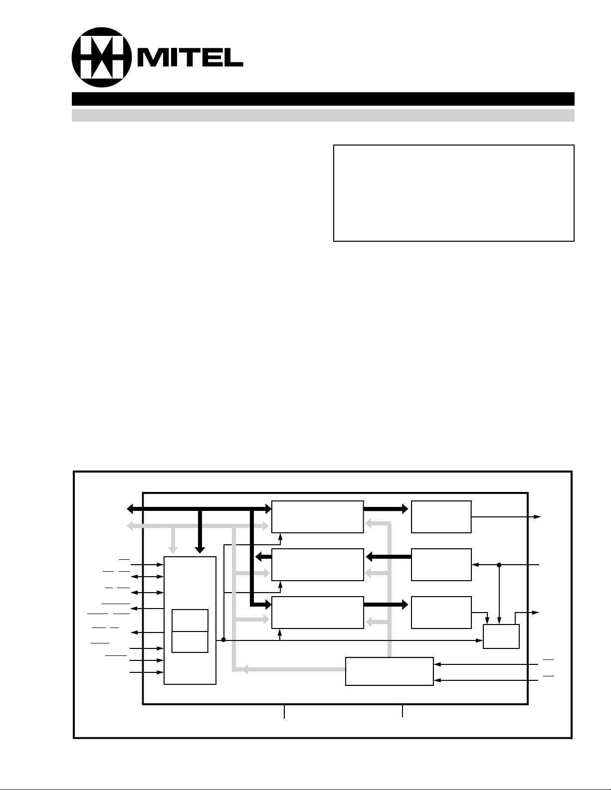
The ST-BUS Parallel Access Circuit (STPA) provides
a simple interface between Mitel’s ST-BUS and
parallel syst em environments.
D7-D0
A4-A0
CS
DS, OE
R/W, WE
DTACK,
BUSY, DCS
IRQ, 24/32
, MS1
IACK
A5, STCH
MMS
Parallel
Port
Interface
Interrupt
Registers
Control
Registers
Tx0
Dual Port Ram
32 X 8
Rx0
Dual Port Ram
32 X 8
Tx1
Dual Port Ram
32 X 8
Address
Generator
V
SS
V
DD
Figure 1 - Functional Block Diagram
Parallelto-serial
Converter
Serial-to-
Parallel
Converter
Parallelto-Serial
Converter
Comp/
MUX
STo0
STi0
STo1
F0i
C4i
3-3
3
Page 2
MT8920B CMOS
1
C4i
2
F0i
IACK, MS1
STi0
DS, OE
R/W, WE
A5, STCH
VSS
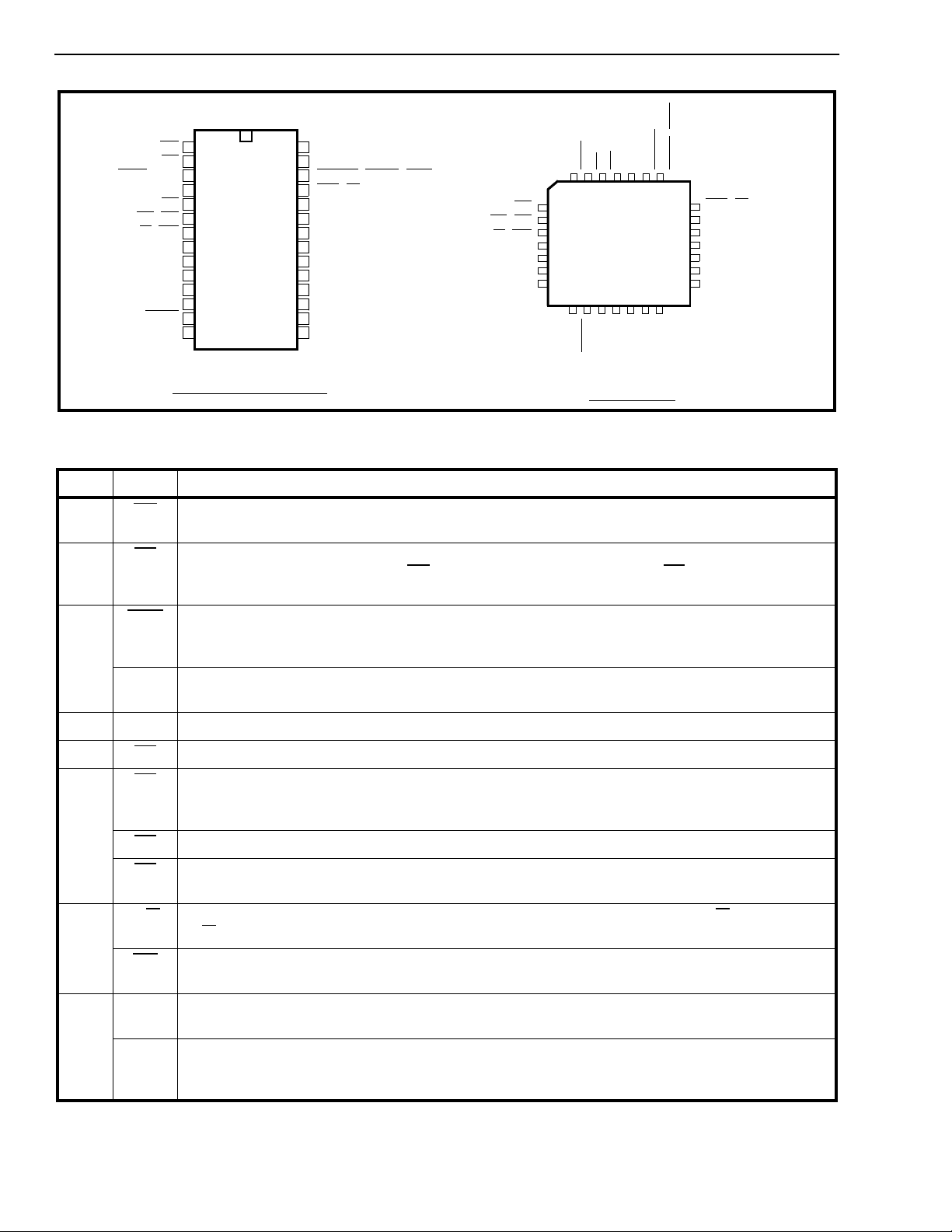
Pin Description
3
4
5
CS
6
7
A0
8
A1
9
A2
10
A3
11
A4
12
13
14
28 PIN PDIP/CERDIP/SOIC
28
27
26
25
24
23
22
21
20
19
18
17
16
15
VDD
MMS
, BUSY, DCS
DTACK
IRQ, 24/32
STo1
STo0
D7
D6
D5
D4
D3
D2
D1
D0
Figure 2 - Pin Connections
CS
DS, OE
R/W, WE
A0
A1
A2
A3
STi0
432
5
6
7
8
9
10
11
1213141516
A4
28 PIN J-LEAD
IACK, MS1
A5, STCH
F0i
C4i
1
•
D0D3D2
VSS
VDD
28
17
D1
MMS
27
,
DTACK
26
18
, DCS
BUSY
25
24
23
22
21
20
19
IRQ, 24/32
STo1
STo0
D7
D6
D5
D4
Pin # Name Description
‡
1C4i4.096 MHz Clock. The ST-BUS timing clock used to establish bit cell boundaries for the serial
bus.
2F0i
Framing P ul se. A low going pulse used to synchronize the STPA t o the 2048 kbit/s ST-BUS
stream. The first falling edge of C4i
subsequent to the falling edge of F0i identifies the start of
a frame.
3IACK
Interrupt Acknowledge (Mode 1). This active low input signals that the current bus cycle is
an interrupt vector fetch cycle. Upon receiving this acknowledgement, the STPA wi ll
output a user-programmed vector num ber on D
- D7 indicating the source of the interrupt.
0
MS1 Mode Select 1 (Mode 2,3). This input is used to select the device operating modes. A low
applied to this pin will select mode 3 while a high will select mode 2. (Refer to Table 1.)
4STi0ST -BUS Input 0. This is the input for the 2048 kbit/s ST-BUS serial data stream.
5CS
6DS
Chip Select. This active low input is used to select the STPA for a parallel access .
Data Strobe (Mode 1). This active low input indicates to the STPA that valid data is on the data
bus during a write operation or that the STPA must output valid data on the data bus during a
read operation.
OE
OE
Output Enable (Mode 2). This active low input enables the data bus driver outputs.
Output Enable (Mode 3). This active low output indicates that the selected device is to be
read and that the data bus is available for data transfer.
7 R/W
Read/Write (Mode 1,2). This input defines the data bus transfer as a read (R/W = 1) or a write
= 0) cycle.
(R/W
WE
Write Enable (Mod e 3). This active low output ind icate s the data on t he data bus is to be
written into the selected location of an external device.
8-12 A0-A4 Address Bus (Mode 1, 2). These inputs are used to select the internal registers and two-port
memories of the STPA.
A0-A4 Address Bus (Mode 3). These address outputs are generat ed by the ST PA and reflect the
position in internal RAM where the information will be fetched f rom or stored in. Addresses
generated in this mode are used to access external devices for direct memory t ransfer.
3-4
Page 3
Pin Description (continued)
CMOS MT8920B
Pin # Name Description
‡
13 A5 Address Bit A5 (Mode 1). This input is used to extend the address range of the STPA. A5
selects internal registers when high and Tx/Rx RAM’s when low.
A5 Address Bit A5 (Mode 2). This input is used to extend the address range of the STPA. A5
selects Tx0/Rx0 RAM’s when low and Tx1/Rx0 RAM’s when high.
STCH
Start of Channel (Mod e 3). This signal is a low going pulse which indicates the start of an
ST-BUS channel. The pulse is four bits wide and begins at the start of each valid channel.
14 V
SS
Ground .
15-22 D0-D7 Bidi recti onal Data Bus. This bus is used to transfer data to or from the STPA during a write
or read operation.
23 STo0 ST -BUS Output 0. This output supplies the output ST-BUS 2048 kbit/s serial data stream from
Tx0 two-port RAM.
24 STo1 ST-BUS Output 1. In modes 1 and 2 this output supplies the output ST-B US 2048 kbit/s serial
data stream from Tx1 two-port RAM. In mode 3, information arriving at STi0 is output here with
one frame delay.
25 IRQ
Interrupt Request (Mo de 1). This open drain output, when low, indicates when an interrupt
condition has been raised within the STPA.
24
/32 24 Channel/32 Chan ne l Select (Mode 2,3). This input is used to select the channel
configuration in modes 2 and 3. A low applied to this pin will select a 24 (T1) channel mode
while a high will select a 32 (CEPT) cha nnel m ode.
26 DTACK
Data Transfer Acknowledge (Mode 1). This open drain output is supplied by the STPA to
acknowledge the completion of data transfers back to the µP. On a read of the STPA, DTACK
low indicates that the STPA has put valid data on the data bus. On a write, DTACK
low
indicates that the STPA has completed latching the µP’s data from the data b us.
BUSY
BUSY (Mode 2). This open drain output signals that the controller and th e ST-BUS are
accessing the same location in the dual-port RAM’s. It is intended to delay the controller
access until after the ST-BUS completes its access.
DCS
Delayed Chip Se lect (Mo de 3). This low going pulse, which is four bit cells long, is active
during the last half of a valid channel. This signal is used to daisy-chain together two STPA’s in
mode 3 that are accessing devices on the same parallel data bus.
27 MMS Master M ode Select (Re set). This Schmitt trigger input selects bet ween either mode 1 (MMS
= 1), or modes 2and 3 (MMS = 0). I f MMS is pulsed low in Mode 1 operation the control and
interrupt registers will be reset. (Refer to Table 1.) During power-up, the time constant of the
reset circuit (see Fig. 8) must be a minimum of five times the rise time of the power supply.
28 V
‡ Pin Descriptions pertain to all modes unless otherwise stated.
Mode MMS MS1
1 1 N/A µP
2 0 1 Fast RAM
300 Bus
Power Supp ly Input. (+5V).
DD
Mode of
Operation
The STPA provides parallel-to-serial and serial-to-parallel conversions through a
Peripheral
Mode
Mode
Controller
Mode
68000-type interface. Two Tx RAMs and one Rx RAM are available along with full
interrupt capability . 32 channel or 24 channe l support is ava ilable. Control Register 1, bit
D
5
operation.
The STPA provides a fast access interface to Tx0, Tx1 and Rx0 RAMs. This mode is
intended for full parallel support of 24 channel T1/ESF trunks and 32 channel CEPT
trunks. Input 24
channel operation.
The STPA will synchronously drive the parallel bus using the address generator and
provide all data transfer signals. This mode is intended to support 24 or 32 channel
devices in the absence of a parallel bus controller. Input 24
operation, input 24
Function
(RAMCON) = 0 for 32 channel operation and D5 (RAMCON)= 1 for 24 channel
/32 (pin 25) = 0 for 24 channel operation, input 24/32 (pin 25) = 1 for 32
/32 (pin 25) = 0 for 24 channel
/32 (pin 25) = 1 for 32 channel operation.
Ta ble 1. STPA Modes of Op eratio n
3-5
Page 4
MT8920B CMOS
Functional Description
The STPA (ST-BUS Parallel Access) device provides
a simple interface between Mitel’s ST-BUS and
parallel system environments. The ST-BUS is a
synchronous, time division, multiplexed serial
bussing scheme with data streams operating at 2048
kbit/s. The ST-BUS is the primary means of access
for voice, data and control information to Mitel’s
family of digital telecommunications components,
including North American and European digital trunk
interfaces, ISDN U and S digital line interfaces, filter
codecs, rate adapters, etc. The STPA provides
several modes of operation optimized according to
the type of inform ation being handled.
For interfacing parallel data and control information
to the ST-BUS, such as signalling and link control for
digital trunks, the STPA provides a µP access mode
(Mode 1), and looks like a 68000 type peripheral. In
this mode, the device provides powerful interrupt
features, useful in monitoring digital trunk or line
status (i.e., synchronization, alarms, etc.) or for
setting up message communication links between
microprocessors.
To interface high speed data or multi-channel v oice/
data to the S T-BUS for switching or transmission, the
STPA has a high speed synchronous access mode
(Mode 2) and acts like a fast RAM. For voice
storage and forward, bulk data transfer, data
buffering and other similar applications, the STPA
has a controllerless mode (Mode 3) in which it
provides address and control signals to the parallel
bus This is useful for performing direct transfers to
the ST-BUS from external devices such as a RAM
buffer.
The STPA is a two port device as shown in the
functional block diagram in Figure 1. The parallel
port provid es direc t acces s to thr ee dual port RA M’s,
two transmit and one receive. The address, data
and control busses are used to communicate
between the RAM‘s and a parallel environment.
Two parallel-to-serial converters, and one
serial-to-parallel converter interface the dual port
RAM’s to the ST-BUS port of the STPA. This port
consists of two serial output streams and one serial
input stream operating at 2048 kbit/s. This
configuration of two outputs and one input was
designed to allow a single STPA to form a complete
control interface to Mitel’s digital trunk interfaces
(MT8976, MT8978 and MT8979) which have two
serial input and one s erial output control streams.
ST-BUS clocking circuitry, address generator and
various control and interrupt registers complete the
STPA’s functionality.
Modes o f Ope ratio n
The three basic modes of operat ion, µP Peripheral
Mode (Mode 1), Fast RAM Mode (Mode 2) and Bus
Controller Mode (Mode 3) are selected using two
external input pins. These inputs are M MS and MS1
and are decoded as shown in Table 1. Whenever
MMS=1 the device resides in Mode 1. In this mode,
MS1 pin is unavailable and is used for a different
function.
When MMS=0, Modes 2 or 3 are selected as
determined by input MS1. If MS1=1, Mode 2 is
selected and if MS1 =0, Mode 3 is selected.
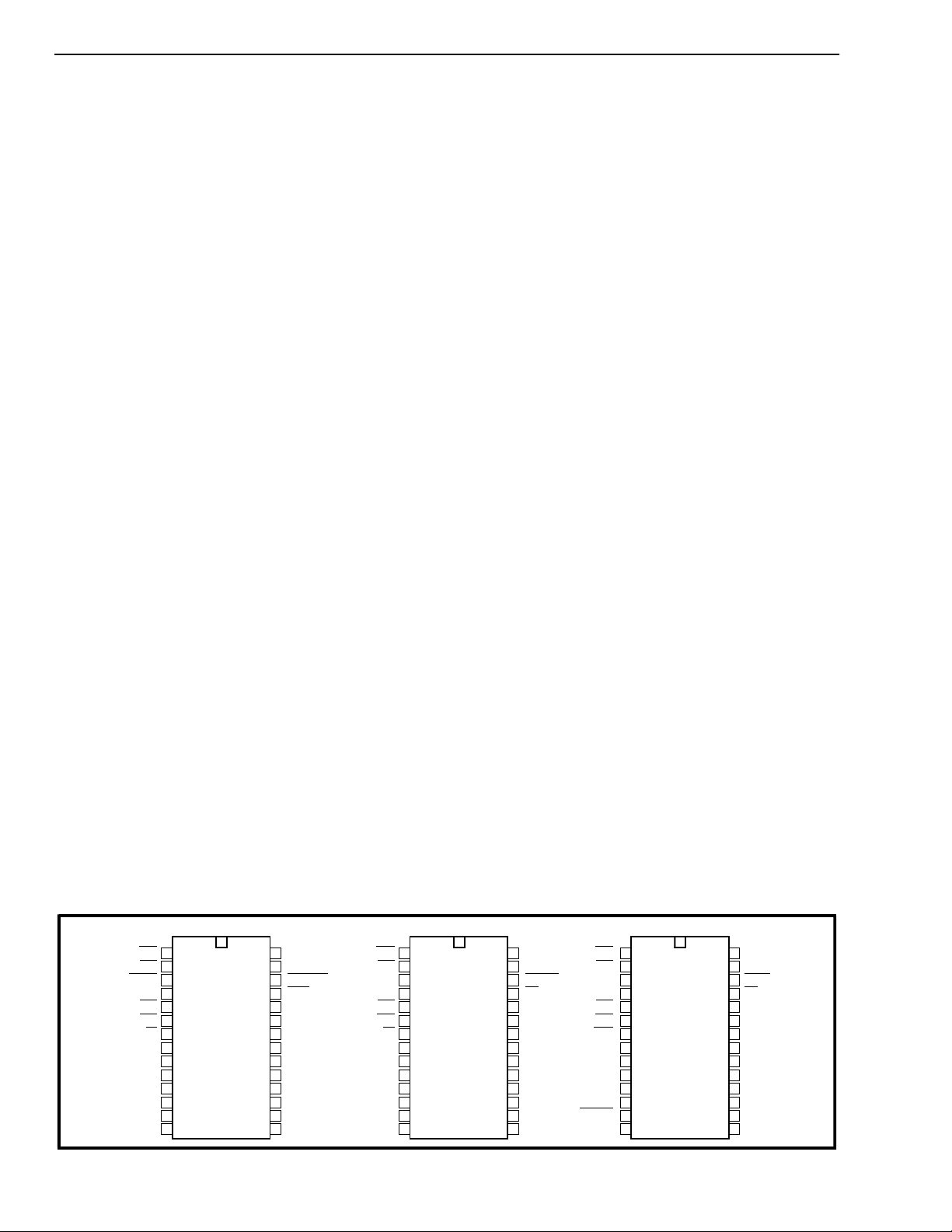
Each of the modes of the STPA provides a different
pinout to ease interfacing requirements of different
parallel environments. These are shown in Figure 3
below. In µP Peripheral Mode the device uses
interface signals consistent with a 68000-type µP
bus. Mode 2, Fast RAM Mode, uses signals typical
of standard RAM type interfaces. Mode 3 interface
signals are very similiar to Mode 2 signals except
that the address and control signals are supplied as
outputs by the STPA.
3-6
µP Peripheral Mode #1
1
C4i
2
F0i
CS
DS
A0
A1
A2
A3
A4
A5
10
11
12
13
14
3
4
5
6
7
8
9
IACK
STi0
R/W
VSS
28
27
26
25
24
23
22
21
20
19
18
17
16
15
Mode #2 Bus Controller Mode #3
1
2
3
4
5
6
7
8
9
28
27
26
25
24
23
22
21
20
19
18
17
16
15
VDD
MMS
BUSY
24/32
STo1
STo0
D7
D6
D5
D4
D3
D2
D1
D0
VDD
MMS
DTACK
IRQ
STo1
STo0
D7
D6
D5
D4
D3
D2
D1
D0
C4i
F0i
MS1
STi0
CS
OE
R/W
A0
A1
A2
A3
A4
A5
VSS
Fast RAM
10
11
12
13
14
Figure 3 - Modes 1, 2, 3 Pin Connections
C4i
F0i
MS1
STi0
CS
OE
WE
A0
A1
A2
A3
A4
STCH
VSS
10
11
12
13
14
1
2
3
4
5
6
7
8
9
28
27
26
25
24
23
22
21
20
19
18
17
16
15
VDD
MMS
DCS
24/32
STo1
STo0
D7
D6
D5
D4
D3
D2
D1
D0
Page 5

CMOS MT8920B
24/32 Chan nel O perat ion
The STPA may be configured to operate as a 32
channel or 24 channel device. This feature, which is
available in all three modes of operation, is
particularly useful in applications involving data
access to CEPT and T1 digital trunk interfaces.
When used as a data interface to Mitel‘s CEPT
digital trunks, the STPA maps the 32 consecutive
bytes of each dual port memory directly to ST-BUS
channels 0-31. This is performed by the address
generator shown in the functional block diagram (see
Figure 1). Figures 4 c & d show the relationship
between relative dual port RAM locations and
corresponding ST-BUS channels, for both input and
output serial streams, when the STPA is configured
as a 32 channel device.
When used as a data interface to Mitel’s T1 trunk
devices, however, only the first 24 consecutive RAM
locations are mapped to 24 of the 32 ST-BUS
channels. This mapping follows a specific pattern
which corresponds with the data streams used by
Mitel‘s T1 products. Instead of a direct correlation
(as in 32 channel operation), the 24 consecutive
RAM locations are mapped to the ST-BUS with every
fourth channel, beginning at channel 0, set to FF
16
(ie. channel 0, 4, 8, 12, 16, 20, 24 and 28). F igures
4 a & b show the relationship between RAM
locations and ST-BUS channel configuration. This
feature allows the STPA to be interfaced directly to
Mitel’s T1 trunk family.
When the STPA is operated in Mode 1, 24 and 32
channel configurations are selected using bit D
(RAMCON) in Control Register 1. D5 = 0 selects 32
channel operation and D
= 1 selects 24 channel
5
operation. When the STPA is operated in Modes 2
or 3, however, the channel configuration is done
using input 24
device uses all 32 channels and when 24
/32 (pin 25). When 24/32 = 1 th e
/32 = 0 it
uses 24.
lessened since ST-BUS accesses require only the
last half cycle of C4i
of every channel. When
contention do e s occur, priority is always given to th e
ST- BUS access.
The STPA indicates this contention situation in a
diff erent manner for Modes 1 and 2. In Mode 1, the
contention is masked by virtue of the
"handshaking" method used to transfer data on
this 68000-type interface. Data Strobe (DS
and Data Transfer Acknowledge (DTACK
the exchange. If contention should occur the
device will delay returning DTACK
and thus stretch
the bus cycle until the µP access can be completed.
In Mode 2, if access is attempted during a
"contention window" the STPA will supply the
BUSY
signal to delay the start of the bus cycle. This
“contention window” is defined as shown in Figure
16. The window exists during the last cycle of C4i
clock in each channel timeslot. Although ST-BUS
access is only required during the last half of this
clock period, the “contention window“ exists for the
entire clock period since a parallel access occurring
just prior to an ST-BUS access will not complete
before the ST-B US access begins. Figure 16 further
shows four possible situations that may occur when
parallel accesses are attempted in and around the
“contention window”. Condition 1 indicates that an
access occurring prior to the contention window but
lasting into the first half of it will complete normally
with no contention arbitration. If the access should
extend past the first half of the contention window
and into the ST-BUS access period, the BUSY
will be generated. Conditions 3 and 4 show accesses
occurring inside the contention window. These
5
accesses will result in BUSY
becoming active
immediately after the access is initiated and
remaining active as shown in Figure 16.
Access contention is non-existent in Mode 3 since
the parallel bus signals, driven by the STPA, are
synchron ize d to th e ST-BUS cl o c ks.
)
) control
signal
Dual Port RAMS
Each of the three serial ST-BUS streams is
interfaced to the parallel bus through a 32 byte dual
port RAM. This allows parallel bus accesses to be
performed asynchronously while accesses at the
ST-BUS port are synchronous with ST-BUS clock.
As with any dual port RAM interface between two
asynchronous systems, the possibility of access
contention exists. The STPA minimizes this
occurrence by recognizing contention only when
accesses are performed at the same time for the
same 8-bit cell within the dual port RAM’s.
Furthermore, the probability of contention is
Mode 1 - µP Peripheral Mode
In Mode 1, the STPA operates as an asynchronous
68000-type microprocessor peripheral. All three
dual-port RAMS (Tx0, Tx1, Rx0) are made available
and may be configured as 32 or 24 byte RA M’s. Also
available are the full complement of control and
inter rupt r egist ers. Th e addr ess ma p for M ode 1 is
shown in Table 2.
The STPA, in Mode 1, uses signals CS
, R/W, DS
(Data Strobe), DTACK (Data Acknowledge) IRQ, and
IACK
(Interrupt Acknowledge) at the parallel interface.
The pin out of the device is s h o w n in Figure 3.
3-7
Page 6

MT8920B CMOS
29 30 31
25 26 27 28
21 22 23 24
17 18 19 20
29 30 31
X
X
X
X
X
25 26 27 28
X
21 22 23 24
X
16
17 18 19 20
X
13 14 15 16
X
9 101112
X
5678
X
1234
0
X
0 1 2 3 4 5 6 7 8 9 10 11 12 13 14 15 16 17 18 19 20 21 22 23
Figure 4 a) RELATIVE Rx RA M ADDRESS vs. ST-BUS CHANNEL - 24 CHAN NEL MODE
13 14 15 16
X
9 101112
X
5678
X
1234
0
X
0 1 2 3 4 5 6 7 8 9 10 11 12 13 14 15 16 17 18 19 20 21 22 23
Figure 4 b) RELATIVE Tx RAM ADDRESS vs. ST-BUS CHANNEL - 24 CHANN EL MODE
0 1 2 3 4 5 6 7 8 9 10 11 12 13 14 15 16 17 18 19 20 21 22 2 3 24 25 26 27 28 29 3 0 31
0 1 2 3 4 5 6 7 8 9 10 11 12 13 14 15 16 17 18 19 20 21 22 2 3 24 25 26 27 28 29 3 0 31
X- unused channe ls m arked X tran smit F F
Figure 4 c) RELATIVE Rx RAM ADDRESS vs. ST-BUS CHANNEL - 32 CHANNEL MODE
0 1 2 3 4 5 6 7 8 9 10 11 12 13 14 15 16 17 18 19 20 21 22 2 3 24 25 26 27 28 29 3 0 31
Figure 4 d) RELATIVE Tx RAM ADDRESS vs. ST-BUS CHANNEL - 32 CHANN EL MODE
0 1 2 3 4 5 6 7 8 9 10 11 12 13 14 15 16 17 18 19 20 21 22 2 3 24 25 26 27 28 29 3 0 31
3-8
STi0
RAM
RELATIVE
LOCATION
STo0
STo1
RAM
RELATIVE
LOCATION
STi0
RAM
RELATIVE
LOCATION
STo0
STo1
RAM
RELATIVE
LOCATION
Page 7

CMOS MT8920B
ADDRESS BITS REGISTERS
A
A
A
A
A
A
6
5
4
3
2
0
0
0
0
0
•
•
•
•
•
•
•
•
•
•
•
•
•
•
•
0
0
1
1
1
A
1
0
0
0
•
•
•
•
•
•
1
1
X 1 0 0 0 0 0 Control Register 1 Control Register 1
X 1 0 0 0 0 1 Control Register 2 Control Register 2
X 1 0 0 0 1 0 Interrupt Vector Register Interrupt Vector Register
X 1 0 0 1 0 0 Interrupt Flag Register 1 X 1 0 0 1 0 1 Interrupt Flag Register 2 X 1 0 0 1 1 0 Image Register 1 X 1 0 0 1 1 1 Image Register 2 X 1 0 1 0 0 0 Interrupt Mask Register 1 Interrupt Mask Register 1
X 1 0 1 0 0 1 Interrupt Mask Register 2 Interrupt Mask Register 2
X 1 0 1 0 1 0 Match Byte Register 1 Match Byte Register 1
X 1 0 1 0 1 1 Match Byte Register 2 Match Byte Register 2
X 1 0 1 1 0 0 Interrupt Channel Address 1 In terrupt Channel Address 1
X 1 0 1 1 0 1 Interrupt Channel Address 2 In terrupt Channel Address 2
1
0
0
0
0
0
0
•
•
•
•
•
•
•
•
•
•
•
•
•
•
•
•
•
•
•
•
•
1
0
1
1
1
1
1
Table 2. Mode 1 Address Map
NOTES:
X is don’t care
A
is bit D4 of Control Register 1
6
READ WRITE
Rx0 - Channel 0
•
•
•
Rx0 - Channel 31
Rx0 - Channel 0
•
•
•
Rx0 - Channel 31
Tx0 - Channel 0
Tx0 - Channel 31
Tx1 - Channel 0
Tx1 - Channel 31
•
•
•
•
•
•
Bit Nam e Descri ptio n
7 (Unused)
6 IRQRST Interrupt Reset. This bit, when set high, automatically clears the Interrupt Flag Register
and the Interrupt Image Register without these registers being serviced. This bit
automatically resets to zero after the register clear is complete d.
5RAMCONRA M Configuration. This bit configures Tx0, Tx1 and Rx0 RAMS for 32 or 24 byte
operation. D
4A
6
Address Bit A6. This bit extends the addressing range for access to Tx1 memory.
= 0 for 32 channel; D5 = 1 for 24 channel.
5
3 IRQ2MODE Interrupt Source 2 Mode Se lec t. This bit configure s the source 2 interrupt generator.
D
= 0 selects “static” interrupt mode; D3 = 1 selects “dynamic” interrupt mode.
3
2 IRQ 1M O DE Interrupt Source 1 Mo de Se lec t. This bit configure s the source 1 interrupt generator.
D
= 0 selects “static” interrupt mode; D2 = 1 selects “dynamic” interrupt mode.
2
1 IRQ2EN Interrupt Sou rce 2 Enabl e. IRQ2EN = 1 enables interrupts to occur from source 2.
0 IRQ1EN Interrupt Sou rce 1 Enabl e. IRQ1EN = 1 enables interrupts to occur from source 1.
Table 3. Control Register 1 Bit Definitions
3-9
Page 8

MT8920B CMOS
Timing information for data transfers on this interface
is shown in Figure 14. The Mode 1 interface is
designed to operate directly with a 68000-type
asynchronous bus but can easily accommodate most
other popular microprocessors as well.
Control Registe rs
Two control registers allow control of Mode 1
features. Control Register 1 provides bits to select
the type of interrupt, to enable interrupts from two
different and independent sources and to reset the
interrupt registers. Also contained in Control
Register 1 are bits to configure the device for 24 or
32 channel operation and to expand the address
range for convenient access to the second transmit
RAM Tx1. A description of the bit functions in
Control Register 1 is shown in Table 3.
Mode 1 provides various loopback paths and output
configuration options which are controlled by bits in
Control Register 2. Bits D
, D1 of Control Register 2
0
configure loopbacks using input and output streams
STi0, STo0 as described in Table 4. The input
stream S Ti0 can be looped back to source the output
stream STo0 as well as receive RAM Rx0. The
transmit RAM Tx0 can be looped to source the
receive RAM Rx0, as well as STo0 and, the transm it
RAM Tx0 can be looped to the receive RAM Rx0
while STi0 sources STo0. The function of these
loopback configurat ions is shown in Figure 5.
In a similar way, the output STo1 can be reconfigured
for different functionality. Bits D
and D3 of Control
2
Register 2 allow STo1 to be sourced, with a one
frame delay via Tx1 from receive stream STi0. STo1
can also output the result of a comparison of the
contents of Tx1 ram wit h input stream STi0. These
output configurations of STo1 are shown in Figure 6
a and b. Figure 6 c shows the effect of combining
these two features.
Interrupt Registers
Interrupts can be generated in Mode 1 only. Two
channels of the ST-BUS input stream, S Ti0, can be
selected to provide an interrupt to the system.
Interrupts can be of two types: Static or Dynamic.
Static interrupts are caused when data within a
selected channel matches a given patte rn. Dynamic
interrupts occur when bits in a selected channel
change state (1 to 0, 0 to 1 or toggle). Interrupts are
controlled through two identical paths (1 and 2)
consisting of the following registers:
Interrupt Channel Address (1/2): The address
(0-31) of the channel which will generate the
interrupt is stored in this register.
Image Register (1/2): The contents of the
channel causing the interrupt is stored in this
register. R eading this register will clear its contents.
Match Byte Register (1/2): In static mode this
register is used to store the byte which will be
compared with the contents of the selected channel
causing the interrupt.
In dynamic mode, the bits in this register and the
corresponding bit in the Interrupt Mask Register
define the type of dynamic interrupt (i.e., 0 to 1, 1 to
0, toggle ). ( R ef er to Table 5.)
Bit Name Description
7-4 (Unused)
3-2 CONFIG STo1 Output Configuration Bits:
D
= 00- Normal operation. ST-BUS stream from Tx1 is output on STo1 pin.
3D2
01- S Ti0 stream is output on STo1 pin delayed one fram e (Figure 6 a).
10- S Ti0 is compared through XOR (exclusive OR) with ST-BUS stream
from Tx1 and output at STo1 (Figure 6 b).
11- STi0 stream, delayed one frame (via Tx1), is compared (XOR) w ith the
next frame arriving at STi0 and the result output at STo1 (Figure 6 c).
1-0 LOOPBACK Internal Loopback Con figuration Bits:
= 00- Normal operation. No internal loo ps.
D
1D0
01- L oo p STi0 to STo0 while still receiving STi0 in Rx0 (Figure 5 a).
10- L oo p Tx0 output ST-BUS stream to Rx0 input ST-BUS stream while
outputting Tx0 outpu t to STo0. STi0 is not received (Figure 5 b).
11- Loop Tx0 output ST-BUS stream to Rx0 input ST-B US stream. Loop
STi0 to STo0 (Figure 5 c).
Table 4. Control Register 2 Bit Definitions
3-10
Page 9

Control Register 2
= 0, D0 = 1
Bits D
1
µP
Control Register 2
Bits D
= 1, D0 = 0
1
µP
Tx0
Rx0
CMOS MT8920B
Control Register 2
= 0, D2 = 1
Bits D
3
µP
STo0
STi0Rx0
a)
Control Register 2
Bits D
= 1, D2 = 0
3
STo0
STi0
µP
Tx0
Rx0
Tx1
Tx0
Rx0
Tx1
1 Frame Delay
a)
STo0
STi0
STo1
STo0
STi0
STo1
b)
Control Register 2
= 1, D0 = 1
Bits D
1
Tx0
µP
Rx0
c)
STo0
STi0
Figure 5 - Loopback Configurations
Interrupt M ask Re g is t e r (1/ 2) : In st at ic m o de th e
contents of th i s reg ister masks bits in th e Ma tch By te
Register that are ’don’t care’ bits
1 - bit masked
0 - bit not masked
In dynamic mode, each bit in this register and the
corresponding bit in the Match Byte Register define
what type o f dynamic inte rrupt is selec ted. (Refer to
Table 5.)
Interrupt Flag Register (1/2): In static mode
the least significant bit in this register is set to 1 to
flag the corresponding path in which the interrupt
occurs.
b)
Control Register 2
= 1, D2 = 1
Bits D
3
µP
Tx0
Rx0
Tx1
1 Frame Delay
c)
STo0
STi0
STo1
Figure 6 - STo1 Configurations
Interrupt Vector Register
This register shown in Figure 7 is common to both
interrupt paths and stores an 8 bit vector number
which will be output on the data bus when
Interrupt Acknowledge (IACK
labelled V
- V7 are stored by the controlling µP.
2
) is asserted. Bits
Bits IRQ1 and IRQ 2 are s et by t he STPA to indica te
which path caused the interrupt. This creates unique
vectors which are used by the µP to vector to
interrupt service routines. This feature may be
bypassed by simply not asserting IACK
during
interrupt ac knowledged.
D7 D6 D5 D4 D3 D2 D1 D0
In dynamic mode this register sets the bits which
reflect the position of the bits in the corresponding
Interrupt Reg i ster which cau sed th e i nt erru pt.
V
V
V
V
7
6
5
V
4
3
Figure 7 - Interr upt Vector Registers
V2IRQ2 IRQ1
3-11
Page 10

MT8920B CMOS
Interrupt Modes and Servicing
Static Interrupt Mode
A static interrupt is caused when an incoming byte
matches a predefined byte. The incoming byte from
a selected channel is stored in Interrupt Image
Register (1 /2 ) w h e re it i s compared wi th th e con te n ts
of the corresponding Match Byte Register. The
result of the comparison of individual bits is masked
by the contents of the Mask Register (1/2) before it
is used t o generate an IRQ
. After a static interru pt
occurs, information in the Interrupt Image Register is
frozen until the µP performs a read operation on this
register.
When servicing static interrupts assertion of IACK
will cause the contents of the Vector Register, with
the IRQ1 o r IR Q 2 b i t set, to be ou tpu t o n th e d a ta
bus. The service routine can subsequently clear IRQ
by reading the Interrupt Image Register.
Alternatively, the IRQRST bit in Control Register 1
can be set to clear the associated interrupt regist ers.
Static Interrupts are selected using IRQ1MODE and
IRQ2MODE bits in Control Register 1. Interrupts are
then enabled to t h e IRQ
pin with IRQ1EN and
IRQ2EN bits of the same register.
Dynamic Interrupt Mode
A dynamic interrupt is generated by a change of
state of bits in a selected channel. A 0 to 1 transition
or a 1 to 0 transition or a simple change of state from
the previous state (toggle) can be detected. The
type of transition to be detected is selected using two
bits, one from the Match Byte Register (1/2) and one
from the Interrupt Mask Register (1/2), in the
corresponding bit positions. Table 5 shows how the
two registers are programmed.
Match
Byte
Register
bit D
X
Mask
Byte
Register
bit D
X
Transition Type Detected
on Incoming bit D
X
(x = 0 ....7)
D
7D6D5D4D3D2D1D0
Channel Address Register 1 =
(channel 4 of STi0 selected)
Match Byte Register 1 =
Interrupt Mask Register 1 =
(When bit D
00000100
00000000
00001000
toggles 0 to 1)
3
Dynamic interrupts from interrupt path 1 would then
be enabled using the Control Register 1.
Control Reg iste r 1 =
00000101
This would cause interrupt 1 path to be enabled
while interrupt 2 path is disabled.
As with sta tic i n terr up ts , u pon se rv ing a dyn am i c
interrupt, assertion of IACK
wil l c aus e the co nt ent s
of the Vector Register, with the appropriate path bit
set, to be output on the data bus. The inform at ion
contained in the channel is frozen in the Interrupt
Image Register. To clear a dynamic interrupt,
however, the µP must read the Interrupt Flag
Register of the path responsible for the interrupt to
determine which bit caused the interrupt. The bit in
the corresponding position will be set to 1 and
reading this register will clear its contents.
Alternatively, as with static interrupts, the IRQRST bit
in Control Register 1 can be set to clear the Image
Interrupt Register, Flag Register and path bits in the
Vector Register.
Dynamic Interrupts are selected using IRQ1MODE
and IRQ2MODE bits in Control Register 1 and are
enabled using IRQ1EN and IRQ2EN in the same
register.
MMS Pin Reset
The STPA can be RESET in Mode 1 using the MM S
pin (27). Applying a low pulse (0V) to MMS after
power is applied to the device will reset all control
and interrupt registers to 00
. This can be
16
accomplished on power up with a simple R-C circuit
as shown in Figure 8.
0
0
1
1
0
1
0
1
Mask Bit D
X
0 to 1 transition
1 to 0 transition
Toggle
Table 5 - Dynamic Interrupt Types
For example, the following steps are required to
generate an interrupt when bit D
of channel 4
3
changes state from 0 to 1 (all ot her bits are masked):
3-12
V
DD
R
MMS
C
STPA
27
Figure 8 - MMS Reset Function
Page 11

CMOS MT8920B
Mode 2 - Fast R AM Mode
Mode 2 operates as a high speed dual port RAM
interface to the ST-BUS. Only the two transmit
RAM’s, Tx0 and Tx1, and the receive RAM, Rx0 are
active in this mode (i.e., control registers and
interrupt registers are inactive).
The main feature of this mode is fast access to the
dual-port RAM’s. Fast access allows high-speed
controllers to use this device as a data interface to
T1 and CEPT digital links. Timing information is
shown i n Fi gu r e 15 .
Mode 2 can also support 24 channel and 32 channel
operation. The channel configuration is selected
using 24
in 24 channel mode and when 24
32 channel mode.
The physical interface in this mode resembles that of
a simple RAM device. The signals used to read
and write the device are CS
the STPA in this mode is shown in Figure 3. Address
decoding for Tx0, Tx1, Rx 0 is shown in Table 6.
Contention can arise for access to the dual port
RAMS. The occurrence of this is minimized since
the ST-BUS serial-to-parallel and parallel-to-serial
converters require RA M access for only 1/32 of
a channel time (i.e., last half cycle of C4i for
each channel). For contention to occur the high
speed controller must access the same RAM
location as that of the ST-BUS. For a parallel read
operation this corresponds to the current ST-BUS
channel and for a write operation, the next ST-BUS
channel. Access contention in Mode 2 is arbitrated
with the BUSY
off any parallel access cycle until it again goes
inactive. Figure 16 shows how the access is
arbitrated for accesses near the co ntention window.
Applications using high speed access can easily
avoid generating BUSY
/32 pin. When 24/32=0 the device operates
/32=1, it operates in
, OE, R/W. The pinout of
signa l. BUSY is intended to hold
by co-ordinating channel
reads and writes with framing and channel boundary
information.
Mode 3 - Parallel Bus C ontroller
In this mode the STPA outputs all necessary signals
required to drive devices attached to the parallel
port. The STPA can be used to drive devices such
as RAM’s, FIFO’s, latches, A/D and D/A converters,
and CODECS, directly from the ST-BUS without an
intervening µP. As with the other modes, Mode 3
can operate from 32 channels or 24 channels by
connecting 24
allows devices to be driven remotely via a T1 or
CEPT digital trunk link when used with Mitel’s trunk
products.
Referring to Figure 1, the Address Generator block
generates and drives the external address lines
A4-A0. The STPA also generates OE
enable) and WE
transfers f rom Rx0 RAM and to Tx0 RAM. Tx1 RAM
is unavailable in this mode.
The STPA, in Mode 3, generates exte rnal addresses
in a particular sequence that minimizes throughput
delay through the device. When channel N is
present on the ST-BUS, the STPA generates
address N+1 on the address bus and asserts OE
to output data from an external device and latch it
into the STPA. During the same channel N, the
STPA will generate address N-1 with WE
to write from the STPA to an external device. Timing
for Mode 3 transfers is shown in Figure 17. All
parallel bus signals are synchronized to the ST- BUS
clock.
The device must be selected using CS
the parallel bus drivers to be enabled. CS
remain active for four ST-BUS bit periods (8 x C4i
cycles) since a read and a write operation require 2
bit periods each. The STPA generates a signal STCH
(start of channel) which becomes active at the start
of each channel and remains active for 1/2 of the
channel time (Figure 18). This signal may be
/32 high or low, respectively. This
(output
(write enable) to facilitate data
asserte d
in order for
should
ADDRESS BITS REGISTERS
A
A
5
0
•
•
•
0
1
•
•
•
1
A
4
0
•
•
•
1
0
•
•
•
1
A
3
0
•
•
•
1
0
•
•
•
1
A
2
0
•
•
•
1
0
•
•
•
1
A
1
0
•
•
•
1
0
•
•
•
1
0
0
•
•
•
1
0
•
•
•
1
READ WRITE
Rx0 - Channel 0
•
•
•
Rx0 - Channel 31
Rx0 - Channel 0
•
•
•
Rx0 - Channel 31
Tx0 - Channel 0
•
•
•
Tx0 - Channel 31
Tx1 - Channel 0
•
•
•
Tx1 - Channel 31
Table 6. Mode 2 Address Map
3-13
Page 12

MT8920B CMOS
connected directly to CS to enable the device
appropriately.
Common Bus
CS
OE
WE
A0
A1
A2
A3
A4
MMS MS1 24
OE
WE
A0
A1
A2
A3
A4
MMS MS1 24
STCH
/32
00 1
CS
DCS
/32
00 1
STi0
STo0
STi0
STo0
Figure 9 - "Daisy-chained" STPA’s in 32 Channe l
Parallel Bus Controller Mode (Mode 3)
In order to fa cilitate effic ient use of th e parallel bu s
another signal, similar to STCH
STPA. Delayed Chip Select (DCS
, is supplied by the
) becomes active
for the last half of each channel (Figure 19). This
may be connected to a second STPA, residing on the
same physical parallel bus, enabling it to perform its
read/write operations in the second half of each
channel. This allows a large number of devices,
connected on a common bus, to be driven by two
ST-BUS streams. Figure 9 shows how this "daisy
chaining" of STPA’s is implemented while Figure 10
illustrates the timing on the shared parallel bus.
Applications
Parallel PBX to Digital Trunk Interface
The STPA is an ideal component for interfacing
parallel PBX environments to Mitel’s family of digital
trunk devices.
Figure 11 shows a typical int erface for both T1/ESF
and CRC-4 CEPT digital trunks to a system utilizing
a parallel bus architecture. Both the MH89760B
T1/ESF and the MH89790B CRC-4 CEPT trunk
modules are shown interfaced to a parallel bus
structure using two STPAs operating in modes 1 and
2.
The first STPA operating in mode 2 (MMS=0,
MS1=1, 24
information betw een the parallel telecom bus and the
T1 or CEPT link via DSTi and DSTo. The second
STPA, operating in mode 1 (MMS=1) provides
access from the signalling and link control bus to the
MH89760B or MH89790B status and control
channels. All signalling and link functions may be
controlled easily through the STPA transmit RAM’s
Tx0, Tx1, while status information is read at receive
RAM Rx0. In addition, interrupts can be set up to
notify the system in case of slips, loss of sync,
alarms, violations, etc.
/32=0), routes data and/or voice
3-14
ST-BUS
C4i
Address
OE
WE
Data Bus
STCH
DCS
CHANNEL N
BIT 7 BIT 6 BIT 5 BIT 4 BIT 3 BIT 2 BIT 1 BIT 0
N + 1 N - 1 N + 1 N - 1
IN OUT IN OUT
Figure 10 - Timing Relationship for Mode 3 Daisy Chaining
Page 13

CMOS MT8920B
†
MH89760B/790B
12.355
MHz Osc.
DIP
Switch
EQU
†
MH89761*
16.388
MHz Osc.
MT8940
†
C2o
F0b
C4b
C1.5o†F0i
Tx
Line
Driver
TxA
TxB
MT8977/79
DSTi
DSTo
CSTi0
CSTo
Rx
Line
Receiver
RxA
RxB
†
CSTi1
F0i
C2i
C1.5i
RxD
E8Ko
)
††
(E2i
†
Clock
Extractor
E1.5i
C8Kb
††
+5V
F0i
STi0
STo0
STo1
(Mode 2)
MT8920B
-D
D
7
0
HIGH
5
-A
0
A
SPEED
PARALLEL
C4i
CS
R/W
OE
BUS
TELECOM
†
+5V
(Mode 1)
MT8920B
MMS MS1 24/32
-D
D
STi0
STo0
STo1
7
5
-A
0
0
A
CS
DS
AND LINK
CONTROL
SIGNALLING
R/W
BUS
C4i
DTACK
F0i
+5V
MMS
IRQ
IACK
NOTES:
† Signals applicable to T1-ESF applications using MT8977 and MH89760B
†† Signals applicable to CRC-4 CEPT applications using MT8 979 and MH89790B
* Equalizer MH89761 available for T1/ESF applications
Figure 11 - Typical T1-ESF / CRC-4 CEPT Digital Trunk Configuration
3-15
Page 14

MT8920B CMOS
Digital Signal Processor to ST-BUS Interface
Mode 2 allows many high speed devices to be easily
connected to the ST-BUS. Figure 12 shows a
TMS32020 digital signal processor interfaced to the
ST-BUS through the STPA. This simple interface
allows com plex functions to be implemented in such
systems as PBX’s and computer systems. Some of
the possi b le fu nc tio n s i n cl u d e:
- D igital Filtering
- Voice Conferencing
- Speech/Data Compression
-Encryption
- Tone Detection and Generation
- Frequency Spectrum Analysis
- Image Processing
- µ-Law to A-Law Conversion
- E cho Cance llation
- Modulation
- Speech Synthesis and Recognition
TMS32020
A8-A0
D7-D0
STRB
READY
DS
RW
MSC
A9
A8
A7
A6
74HCT
138
E2
E1
A
B
C
MT8920B
CS
A5-A0
D7-D0
OE
WE
MMS MS1 24
+5V +5V
STo0
STi0
STo1
/32
3-16
Figure 12 - ST-BUS to DSP I nterface
Page 15

CMOS MT8920B
Connect ing the STPA to a shared S T-BUS Line
The STPA’s STo0 and STo1 outputs cannot be
directly forced into a high impedance state.
However, with some external logic, the STo0 output
can be buffered by a three-state device, controlled
by the STo1 output. This application is only possible
if the Tx1 RAM and associated STo1 output are not
required for some other purpose.
Figure 13 shows an ext ernal buffer U1 controlled by
the STo1 output and an external Output Data Enable
(ODE) signal. When FF (hex) is written to the Tx1
RAM, the corresponding STo1 output channel goes
to logic high. This signal, AND-ed together with a
logic high at ODE, enables U1, resulting in the STo0
signal transparently passed to the output of U1.
When 00 (hex) is written to the Tx1 RA M, the STo1
output goes logic low. This disables U1, resulting in
a high impedance state at the output of U1,
corresponding to the selected channel.
This method of three-state buffering permits output
control on a per-channel or per-bit basis.
The ODE input is used to enable the ST-BUS outputs
after all ST-B US devices are properly configured by
software. This eliminates the possibility of
contention on the ST-BUS lines during the power-up
state.
Parallel Port
ODE
Parallel Port
STo0
MT8920B
STo1
ODE
STi0
STi1
STi7 STo7
STo0
STo1
MT8980
74HC00
74HC125
U2
U1
ST-BUS
Figure 13 - Co nnecti ng STPA to a Common ST-BUS Line
3-17
Page 16

MT8920B CMOS
Absolute Maximum Ratings * - V oltages are with respect to ground (V
) unless otherwise stated.
SS
Parameter Symbol Min Max Units
1 Supply Voltage V
DD
2 Voltage on any I/O pin -0.3 V
3 Current on any I/O pin I
4 Storage Temperature T
5 Package Power Dissipation Cerdip
Plastic
* Excee di ng these values may cause pe rman ent dama ge. Functi on al operati on under these co ndition s is not implie d.
I/O
ST
P
D
P
D
Recommended Operating Conditions - Voltages are with respect to ground (V
Characteristics Sym Min Typ
1 Supply Voltage V
2 Input High Voltage V
3 Input Low Voltage V
4 Operating Tem perat u re T
5 Operating Clock Frequency f
‡ Typical figures are at 25°C and are for design aid only: not guaranteed and not subject to producti on testing.
CK
4.75 5.0 5.25 V
DD
2.4 V
IH
IL
A
0 0.4 V for 400mV noise margin
-40 25 85 °C
‡
4.096 MHz
-0.3 7.0 V
+ 0.3 V
DD
±25 mA
-55 125 °C
1000
600
) unless otherwise stated.
SS
Max Units Test Conditions
DD
V for 400mV noise margin
mW
mW
DC Electrical Characteristics - Voltages are with respect to ground (V
) unless otherwise stated .
SS
Characteristics Sym Min Typ‡Max Units Test Con di tion s
1 Supply Current Static
Dynamic
2 Input High Vol tage V
3 Input Low Voltage V
4 Input Leakage Current I
I
CCS
I
CCD
10
510
2.0 V
IH
IL
Z
0.8 V
±10 µAVDD=5.25V,
µAmAoutputs unloaded
@f
V
5 Input capacitance C
6 Schmitt trigger input high (MMS) V
7 Schmitt trigger input low (MMS) V
8 Schmitt trigger hysteresis (MMS) V
9 Output high current (except IRQ
10 Output low current (except IRQ
11 IRQ
12 Tristate Leakage A
, DTACK, BUS Y Sink Current I
, OE, WE
4-A0
) I
)IOL510 mAVOL = 0.4V, VDD = 4.75V
I
IN
T+
OH
OL
OZ
3.8 3.0 V
T-
0.8 1.0 V
H
2.0 1.0 V
10 15 mA V
10 15 m A VOL = 0.4V, VDD = 4.75V
±1 ±10 µAVDD = 5.25V
(mode 3)
13 Open drain off-state current
IRQ
, DTACK, BUSY
14 Output capacitance C
‡ Typical figures are at 25°C and are for design aid only: not guaranteed and not subject to producti on testing.
I
OFF
±1 ±20 µAVDD = 5.25V
O
10 pF
V
V
15 pF
= 4.096 MHz
CK
IN=VSS to VDD
= 2.4V, VDD = 4.75V
OH
= VSS to V
OUT
OUT
= V
DD
DD
3-18
Page 17

CMOS MT8920B
AC Electrical Characteristics†- Mode 1 Parallel Bus Timing (see Fig. 14)
(VCC=5.0V ±5%,TA=-40 to 85°C)
Characteristics Sym Min Typ
††
††
††
t
ARDS
t
RWDS
t
RDS
RD
0ns
20 ns
1,2
t
cwmtCLK
t
cwm
1 Address to DS
2R/W
3DS
to DS (CS) Low
(CS) Low to DTA CK Low
(CS) Low
4 Valid Data to DTACK Low (Read) t
-30
5DS High to DTACK High t
6DS High to Data High Imped.(Read) t
7DS High to CS High t
8 Data Hold Time (Write) t
9 Input Data Valid after DS
DD
††
=5V, t
=244 ns, tCH=tCL=122 ns and are for design aid only: not guaranteed and not subject to production
CLK
or DS, whichever occurs last. Timing is relative to the last falling edge which initiates the cycle.
10 Address Hold Time
† Timing is over recommended temperature & power supply voltages.
‡ Typical figures are at 25°C, V
testing.
††The cycle is initiated by the falling edge of CS
(1) t
is equal to tCH or tCL whiche ve r is smaller (some ST-BUS com pa tible trans ceiv ers may gener ate C 4 clock having t
cwm
or t
(2) Worst case access when memory contention occurs.
CLmin
=90ns.
DAR
DHZ
CSH
DHT
t
DST
t
ADHT
045ns
0ns
0ns
50 ns
‡
Max Units Test Conditions
2*t
CLK
65 ns
t
cwm
ns
ns
ns
Load C
Load A, CL=130pF, RL=740Ω
Load C, CL=50pF
Load A, CL=130pF, RL=740Ω
-30
CHmin
=90ns
A0 - A5
(IACK†)
CS
R/W
DS
DTACK
D0 - D7
t
RWDS
t
ARDS
t
DST
t
ADHT
t
RDS
t
CSH
t
DAR
t
RD
DATA OUT
t
DHT
t
DHZ
D0 - D7
DATA IN
Figure 14 - Mode 1 Parallel Bus Timing
† During Int errupt Acknowled g e cycle IAC K replaces CS. R/W must remain high.
3-19
Page 18

MT8920B CMOS
AC Electrical Characteristics† - Mode 2 Par allel Bus Timing - (see Figures 15 and 16)
(VCC=5.0V ±5%,TA=-40 to 85°C)
Characteristics Sym Min T yp
‡
Max Units Test Conditions
1OE
2 Address Access Time t
3CS Low to Valid Data t
4 Output Disable t
5 Address Setup Time t
6 Data Setup Time t
7 Data Hold Time t
8 Address Hold Time t
9 Write Pulse Width t
10 OE
11 OE
12 C4i
13 C4i Low to Busy High t
14 OE, R/W High to Busy Low t
† Timing is over recommended temperature & power supply voltages.
‡ Typical figures are at 25°C, V
testing.
Low to Valid Data t
, R/W High to C4i High t
, R/W Low to C4i Low t
High to Busy Low t
DD
=5V, t
=244 ns, tCH=tCL=122 ns and are for design aid only: not guaranteed and not subject to production
CLK
EVD
AA
CSD
50 ns
OHZ
ASF
DST
DHT
AH
WP
EC4H
EC4L
C4BL
C4BH
EBL
20 ns
30 ns
5ns
50 ns
50 ns
60 ns
120 ns
60 ns
-10 ns
10 ns
50 ns
50 ns
40 ns
Load A, CL=130pF, RL=740Ω
Load A, CL=130pF, RL= 740Ω
Load A, CL=130pF, RL=740Ω
Load A, CL=130pF, RL=740Ω
Load C
Load C
Load C
A0 - A5
CS
OE
R/W
D0 - D7
t
AH
t
ASF
t
WP
t
OHZ
t
EVD
t
CSD
t
AA
t
Figure 1 5 - Mode 2 Timing Diagram (No Contention)
DST
t
DHT
DATA INDATA OUT
3-20
Page 19

CMOS MT8920B
C4i
A0 - A5
CS
CONDITION 1:
OE, R/W
BUSY
CHANNEL N - BIT 0
CHANNEL (N + 1) - BIT 7
ST-BUS ACCESS
CONTENTION WINDOW
READ ADDRESS N or WRITE ADDRESS (N + 1)
(N matches incoming
ST-BUS channel)
Access begin s before conte nt ion wind ow an d finishe s before ST-BUS access - No conten tion.
t
EC4H
CONDITION 2:
OE, R/W
BUSY
CONDITION 3:
OE, R/W
BUSY
CONDITION 4:
OE, R/W
BUSY
Access begins before contention window and continues into ST-BUS access.
t
EC4L
t
C4BL
Access begins within contention window bu t before ST-BUS access.
t
EC4L
t
t
EBL
C4BH
Access begins during ST-BUS access
t
EBL
t
C4BH
t
C4BH
Figure 16 - Mode 2 Access Contention Resolution
3-21
Page 20

MT8920B CMOS
AC Electrical Characteristics† - Mode 3 Timing (see Fig.17, 18 and 19)
((VCC=5. 0V ±5%,TA=-40 to 85°C)
Characteristics Sym Min Typ
‡
Max Units Tes t Condi tions
1CS
2C4i Low to Address Change t
3CS to OE, WE, Address Disabled t
4C4i Low to Output Enable Low t
5C4i Low to Output Enable High t
6OE, WE, Pulse Width t
7C4i Low to Write Enable Low t
8C4i Low to Write Enable High t
9 Read Data Valid f rom OE t
10 Read Dat a Hold Time t
11 Write Data Setup Time t
12 Writ e Data Hold Time t
13 C 4i Transition to STCH, DCS Trans. t
14 STCH Pulse Width t
15 DCS Pulse Width t
† Timing is over recommended temperature & power supply voltages.
‡ Typical figures are at 25°C, V
testing.
to OE, WE, Address Enabled t
DD
=5V,t
=244ns, tCH=tCL=122ns and are for design aid only: not guaranteed and not subject to production
CLK
ZR
ACS
RZ
OED
OEH
ENPW
WED
WEH
(2*t
RST
RHT
WST
WHT
STC
SCPW
CSPW
0ns
70 100 ns
70 100 ns
50 ns
110 ns
50 ns
75 ns
75 ns
2*t
CLK
75 ns
75 ns
)
CLK
-60
120 ns
1830 ns
1830 ns
Load A, CL = 130pF, RL = 740Ω
Load A, CL = 130pF, RL = 740Ω
Load A, CL = 130pF, RL = 740Ω
Load A, CL = 130pF, RL = 740Ω
Load A, CL = 130pF, RL = 740Ω
Load A, CL = 130pF, RL = 740Ω
ns
Load A, CL = 130pF, RL = 740Ω
Load A, CL = 130pF, RL = 740Ω
ns
Load A, CL = 130pF, RL = 740Ω
Load A, CL = 130pF, RL = 740Ω
Load A, CL = 70pF, RL = 1.2 2KΩ
Load A, CL = 70pF, RL = 1.2 2KΩ
Load A, CL = 70pF, RL = 1.2 2KΩ
C4i
A4 - A0
OE
WE
D7 - D0
CS
CHANNEL N
BIT 7 (BIT 3) BIT 6 (BIT 2) BIT 5 (BIT 1) BIT 4 (BIT 0)
t
ACS
N + 1 N - 1
t
OED
t
ENPW
t
RST
DATA IN DATA OUT
t
ZR
t
OEH
t
RHT
t
WST
t
WED
t
ENPW
t
WEH
t
WHT
t
RZ
3-22
Figure 17 - Mode 3 Timing Diagram
Page 21

CMOS MT8920B
CHANNEL N-1
C4i
STCH
CHANNEL N
BIT 0 BIT 7 BIT 6 BIT 5 BIT 4
t
STC
t
SCPW
t
STC
Figure 1 8 - Mode 3 STCH Timing Diagram
CHANNEL N CHANNEL
BIT 4 BIT 3 BIT 2 BIT 1 BIT 0
C4i
STCH
DCS
t
STC
t
CSPW
Figure 19 - Mode 3 DCS
Timing Diag r am
t
STC
N+1
3-23
Page 22

MT8920B CMOS
AC Electrical Characteristics† - ST- BU S Timing (see Figure 20 )
(VCC = 5.0V ± 5%, TA = -40 to 85°C)
Characteristics Sym Min Typ
‡
Max U nits Test Con di tio ns
1 Clock C4i
2 Clock C4i
3 Clock C4i
4C4i
5C4i
Rise Time t
Fall Time t
6 Frame Pulse Setup Time t
7 Frame Pulse Hold Time t
8 STo 0 /1 Dela y from C4i
9 STi0 Setup Time t
10 STi0 Hold Time t
† Timing is over recommended temperature & power supply voltages.
‡ Typical figures are at 25°C, V
Period t
Period High t
Period Low t
=5V and are for design aid only: not guaranteed and not subject to produ ctio n testi ng.
DD
CLK
CH
FPS
FPH
t
SOD
STS
STH
CL
R
F
244 ns
90 122 150 ns
90 122 150 ns
20 ns
12 ns
20 ns
20 ns
100 ns Load B
20 n s
35 n s
C4i
F0i
STo0
STo1
STi0
t
FPS
t
SOD
t
t
CLK
FPH
Bit Cell
t
STStSTH
t
CL
t
CH
t
R
t
F
3-24
Figur e 20 - ST-BUS Tim ing Di agr am
Page 23

125 µs
CMOS MT8920B
CHANNEL
31
INPUTS
OUTPUTS
2.0 V
0.8 V
2.0 V
0.8 V
CHANNEL
0
Bit D
on
Data Bus
CHANNEL30CHANNEL31CHANNEL
(8/2.048) µs
7
BIT 7 BIT 6 BIT 5 BIT 4 BIT 3 BIT 2 BIT 1 BIT 0
Figure 21 - Form at of 20 48 k bit/s ST-BUS Str eam s
0
Bit D
0
on
Data Bus
Figure 22 - Waveform Test Point Reference
V
DD
V
R
L
DD
500Ω
=150pF
C
C
L
6.0k
IN4148
LOAD A
L
=130pF
C
L
LOAD B LOAD C
Figure 23 - Test Load Circuits
3-25
Page 24

MT8920B CMOS
NOTE S:
3-26
 Loading...